Current address: ]Department of Physics, University of California, Santa Barbara, CA 93106, USA
Visualizing supercurrents in ferromagnetic Josephson junctions with various arrangements of and segments
Abstract
Josephson junctions with ferromagnetic barrier can have positive or negative critical current depending on the thickness of the ferromagnetic layer. Accordingly, the Josephson phase in the ground state is equal to 0 (a conventional or 0 junction) or to ( junction). When and segments are joined to form a “ junction”, spontaneous supercurrents around the boundary can appear. Here we report on the visualization of supercurrents in superconductor-insulator-ferromagnet-superconductor (SIFS) junctions by low-temperature scanning electron microscopy (LTSEM). We discuss data for rectangular 0, , , -- and junctions, disk-shaped junctions where the boundary forms a ring, and an annular junction with two boundaries. Within each 0 or segment the critical current density is fairly homogeneous, as indicated both by measurements of the magnetic field dependence of the critical current and by LTSEM. The parts have critical current densities up to at , which is a record value for SIFS junctions with a NiCu F-layer so far. We also demonstrate that SIFS technology is capable to produce Josephson devices with a unique topology of the boundary.
pacs:
74.50.+r, 85.25.Cp 74.78.Fk 68.37.HkI Introduction
As predicted more than 30 years agoBulaevski et al. (1977), Josephson junctions can have a phase drop of in the ground state. Such junctions are now intensively investigated, as they have a great potential for applications in a broad range of devices ranging from classical digital circuitsTerzioglu et al. (1997); Terzioglu and Beasley (1998); Ustinov and Kaplunenko (2003); Ortlepp et al. (2006) to quantum bitsIoffe et al. (1999); Blatter et al. (2001); Yamashita et al. (2005, 2006). Nowadays, Josephson junctions can be fabricated by various technologies, including junctions with a ferromagnetic barrier Ryazanov et al. (2001); Kontos et al. (2002); Blum et al. (2002); Bauer et al. (2004); Sellier et al. (2004); Oboznov et al. (2006); Weides et al. (2006a); Vavra et al. (2006); Bannykh et al. (2009), quantum dot junctionsvan Dam et al. (2006); Cleuziou et al. (2006); Jorgensen et al. (2007) and nonequilibrium superconductor-normal metal-superconductor Josephson junctions Baselmans et al. (1999, 2002); Huang et al. (2002)
In the simplest case the supercurrent density across the junctions is given by the first Josephson relation
| (1) |
with the critical current density for a 0 junction and for a junction. Here, is the gauge invariant phase difference of the superconducting wave function across the junction (Josephson phase).
Particularly superconductor-insulator-ferromagnet-superconductor (SIFS) junctions Kontos et al. (2002); Weides et al. (2006a); Bannykh et al. (2009) are promising since, in contrast to other types of junctions, they exhibit only small damping at low temperatures, which is necessary to study Josephson vortex dynamics as well as to use them as active elements in macroscopic quantum circuits.
Now consider a junction in the – plane, which has a region with critical current density (0 region) and another region having ( region). For the sake of simplicity let us assume that the boundary between and regions runs along the direction. When is different from or the supercurrents flow in opposite directions on the two sides of the 0- boundary, forming a vortex, with its axis coinciding with the 0- boundary (along the direction), that carries a magnetic flux ( is the flux quantum) Bulaevski et al. (1978); Xu et al. (1995); Goldobin et al. (2002). This is true if the junction length in direction is much larger than the Josephson penetration depth
| (2) |
Here is the inductance per square (with respect to in-plane currents) of the superconducting electrodes forming the junction. For junctions having electrode thicknesses larger than the London penetration depth , . Experimentally, such semifluxons have first been studied in the context of cuprate grain boundary junctionsKirtley et al. (1996, 1999) or zigzag ramp junctions between Nb and Hilgenkamp et al. (2003). Here, the sign change of the -wave order parameter of the cuprates leads to the formation of 0- facets. In junctions with a ferromagnetic barrier the value (and the sign) of the critical current density crucially depends on the thickness of the F-layerKontos et al. (2002); Weides et al. (2006a). A junction consisting of various 0 and segments can, thus, be formed by selectively etching the F-layer to produce two thicknesses and of the F-layer such that they correspond to critical current densities and with opposite signs and Weides et al. (2006b).
In the cuprate/Nb zigzag junctions Smilde et al. (2002); Hilgenkamp et al. (2003); Ariando et al. (2005); Gürlich et al. (2009) the facets should be oriented along the crystallographic and axes of the cuprate electrode, imposing certain topological limitations to the 0- boundary. In contrast, the SIFS technology allows almost any 2D shape of the 0- boundary and therefore offers a higher degree of design flexibility. Below, we show an example where this boundary forms a loop. Even intersecting 0- boundaries should be feasible, e.g., by arranging 0 and regions in a checkerboard pattern. Unfortunately, the present SIFS technology based on a NiCu ferromagnetic layer produces a maximum which is much lower than of standard Josephson tunnel junctions. Although at has been increased from some for the first junctionsKontos et al. (2002), to a few in Ref. Weides et al., 2006a and to about in the present paper, the value of is still above . Thus, the study of a multi semifluxon system would thus require unreasonably large (mm sized) junctions.
Nonetheless, also (multifacet) junctions with length are interesting. For example, one can consider an array of many alternating 0 and segments along , where the lengths of individual segments are much smaller than . Such a structure is similar to short multifacet cuprate/Nb zigzag junctionsSmilde et al. (2002); Hilgenkamp et al. (2003); Ariando et al. (2005) or high angle grain boundaries in high cuprates Mannhart et al. (1996) and can e.g. be used to realize a junction — a junction having a phase in the ground state and many other interesting propertiesBuzdin and Koshelev (2003); Goldobin et al. (2007); Mints (1998); Mints and Papiashvili (2001); Mints et al. (2002).
The goal of this work is to realize Josephson junctions with various arrangements of 0 and segments in order to demonstrate that also complex structures are feasible. We characterize these junctions by measurements of current voltage (–) characteristics, by and by low-temperature scanning electron microscopy (LTSEM) Gross and Koelle (1994). By analyzing , in principle one obtains information on the suercurrent flow and (in)homogeneity of the critical current; however, the analysis at least of the more complex SIFS structures may require to consider many unknown parameters (gradients in critical current density, local inhomogeneities etc.), making conclusions ambiguous. We thus put a strong focus on LTSEM which allows direct imaging of the supercurrent density distribution in the junctions (including counterflow areas induced by the segments), close to Gürlich et al. (2009).
The paper is organized as follows. In Sec. II we discuss the sample fabrication and measurement techniques. The experimental results are presented and compared with the numerical simulations in Sec. III. Different subsections are devoted to various geometries, (0 junction for reference, 0- and -- junctions, a junction consisting of 0- regions periodically repeated 20 times, a disk shaped structure where the 0- boundary forms a ring and an annular junction containing two 0- boundaries). All investigated samples are in the short limit (). Finally, Sec. IV concludes this work.
II Samples and measurement techniques
II.1 Sample fabrication
| # | junction | facets | () | () | () | () | ||||
|---|---|---|---|---|---|---|---|---|---|---|
| #1 | 0 | 1 | 50 | 10 | 85 | - | 41 | - | 1.2 | 50 |
| #2 | 1 | 50 | 10 | - | 35 | - | 65 | 0.77 | 18 | |
| #3 | 0- | 2 | 25 | 10 | 85 | 35 | 41 | 65 | 1.0 | 24 |
| #4 | 0--0 | 3 | 16.6 | 10 | 73 | 33 | 44 | 66 | 1.0 | 23 |
| #5 | 40 | 5 | 10 | 37 | 29.5 | 62 | 70 | 3.0 | 11.5 | |
| #6 | 0- disk | 2 | 9; 23.5 | – | 4.6 | 13.4 | 176 | 103 | 0.29 | 6.6 |
| #7 | 0- ring | 2 | 310 | 2.5 | 7.3 | 2.5 | 139 | 239 | 3.5 | 6.8 |
The heterostructures used for our studies were fabricated, as described in Refs. Weides et al., 2006b, 2007. In brief, one starts with a bilayer (Nb thickness is 120) as for usual Nb based Josephson tunnel junctions. The thicknesses of the following F-layer must be chosen very accurately to realize 0 and regions with approximately the same critical current density. To achieve that, first the Ni0.6Cu0.4 F-layer is sputtered onto the wafer with a thickness gradient along the -direction to achieve a wedge-like NiCu layer. Later on, a set of structures extending along and consisting of the 0- devices to be measured, plus purely 0 and reference junctions, is repeated several times along the -direction. One of the sets will have the most suitable F-layer thickness to yield coupling with roughly optimal critical current density. In this way the number of wafer runs which are required to get appropriate 0- junctions is minimized. After the deposition of a 40 nm Nb cap-layer and lift-off one obtains a complete SIFS stack, however without steps in the thickness of the F-layer yet. To produce such steps, the parts of the structures that shall become regions are protected by photo resist. Then the Nb cap-layer is removed by SF6 reactive rf etching, leaving a homogeneous flat NiCu surface, which is then further Ar ion etched to partially remove about 1 of the F-layer. These areas, in the finished structures, realize the 0 regions, while the non-etched regions are regions. To finish the process, after removing the photo resist, a new 40 Nb cap-layer is deposited and, after a few more photolithographic steps the full structures are completed having a 400 thick Nb wiring layer, plus contacting leads and insulating layers. The thickness of the F-layer in the devices used here is and is different for all devices as they come from different places of the chip because of a gradient in the F-layer thickness.
Several sets of 0, , 0-, 0--0 and junctions were fabricated in the same technological run. The disk shaped and annular samples were fabricated during another run. Parameters of the junctions are presented in Tab. 1.
II.2 Measurement techniques and analysis of LTSEM signal
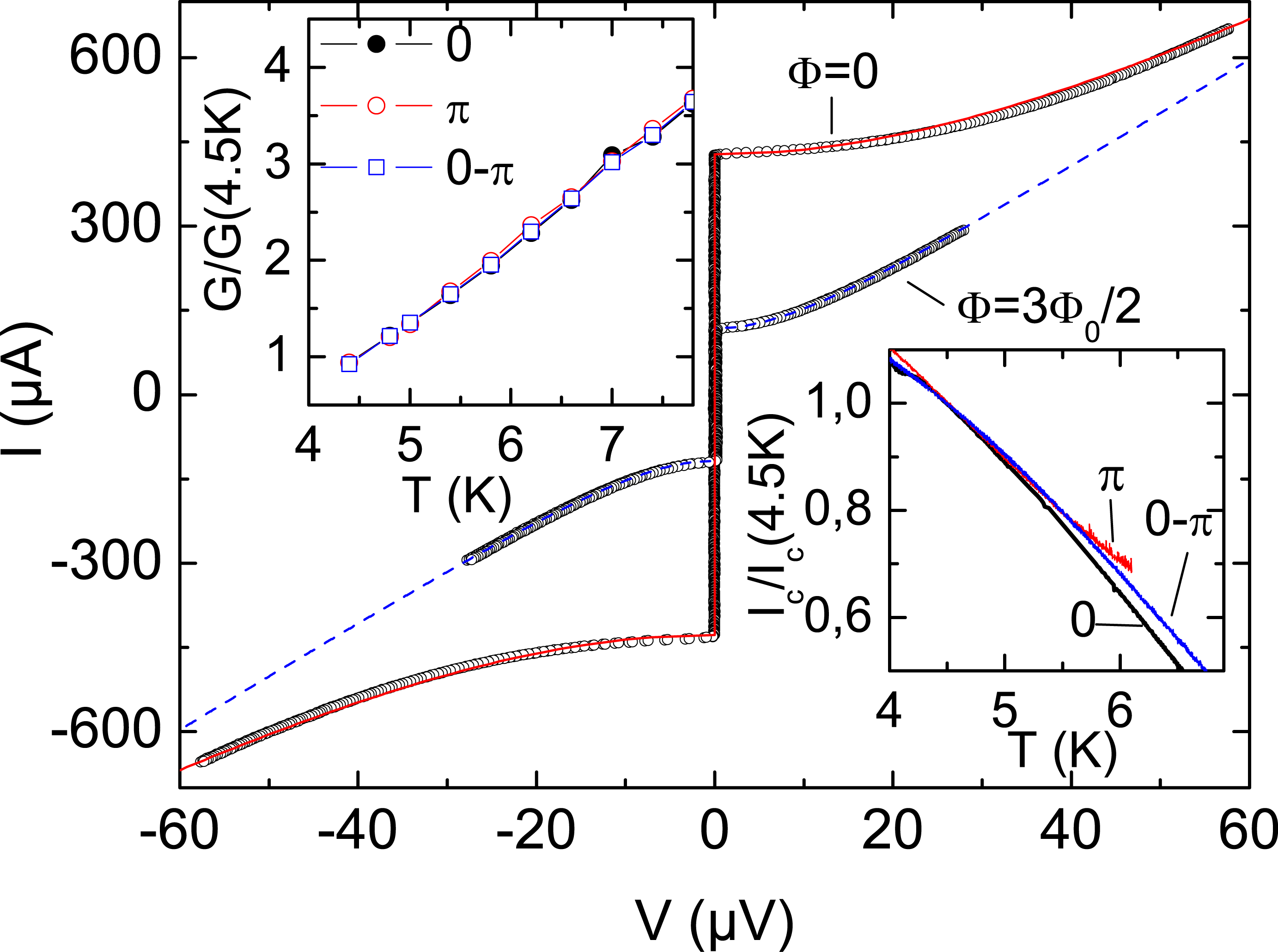
For the measurements the samples were mounted on a LTSEM He cryostage and operated at a temperature . Low pass filters with a cutoff frequency of 12 kHz at 4.2 K, mounted directly on the LTSEM cryostage, were used in the current and voltage leads to protect the sample from external noise. Magnetic fields of up to 1.2 mT could be applied parallel to the substrate plane and thus parallel to the junction barrier layer. We recorded – characteristics and . To detect we used a voltage criterion ( 0.2 for Figs. 3 and 5, 0.5 for Figs. 2 and 4, 1 for all other figures).
For selected values of magnetic field, LTSEM images were taken by recording the electron-beam-induced voltage change across the junctions (current biased slightly above ) as a function of the beam-spot coordinates on the sample surface. The periodically blanked electron beam (using , acceleration voltage , beam current ), focused onto the sample, causes local heating and thus local changes in temperature-dependent parameters like the critical current density and conductivity of the junction. The beam current also adds to the bias current density in the beam spot around , but for all measurements reported here the beam current density is several orders of magnitude below the typical transport current densities. Thus, this effect will be ignored here. The local temperature rise depends on the coordinates , and . For our SIFS junctions the relevant depth is the location of the IF barrier layer, where changes in and affect the – characteristics by changing the critical current and the junction conductance . We describe the temperature profile within the barrier layer of our junctions by a Gaussian distribution
| (3) |
where and is the position of the center of the e-beam. The LTSEM images presented below are reproduced well by simulations using ; this value was used for all calculated images shown below and is somewhat larger than for other LTSEM measurements, presumably due to the relatively thick top Nb layer. Further, from the beam-induced changes of the critical current and the measured temperature coefficient , we estimate . To a good approximation the beam-induced change of critical current is proportional to the beam-induced change of the local Josephson current densityChang and Scalapino (1984), at . To see this we write
Here, the subscripts “on” and “off” refer to electron beam switched on and off. The integral has to be taken over the junction area . The local depends on the coordinates via the Gaussian profile of and possible sample inhomogeneities. In addition, is different in the 0 and parts of the junction, with the values of and at a given temperature. Assuming that the junction is small compared to and that a magnetic field is applied in the plane, with components and along and , the Josephson phase is given by the linear ansatz
| (5) |
At the initial phase is given such that the supercurrent is maximized. For junctions having electrode thicknesses larger than the London penetration depth , the effective junction thickness is . For our Nb electrodes, using we estimate . In general, the phase is different in the “on” and “off” states of the beamChang and Scalapino (1984); Chang et al. (1985). When the electron beam disturbs the junction only slightly this difference may be neglected and we obtain
| (6) |
As can be seen in the lower right inset of Fig.1, at least for some of our junctions the normalized value
| (7) |
(assuming a homogeneous ) is about constant () and roughly the same for 0 and parts. Note, however, that the latter statement, although valid for the junctions we study here, may not always be true. There are cases, e.g. near a temperature driven 0- transition Ryazanov et al. (2001) where of 0 and parts differ strongly in magnitude and perhaps even in sign. Assuming a constant value of we can further write
| (8) |
where we have used the notation
| (9) |
where the brackets indicate the convolution of with the beam-induced Gaussian temperature profile Eq. (3). When the size of the beam-induced perturbation is small compared to the structures to be imaged, we can approximate the Gaussian temperature profile with a -function, and further simplify the above expression to
| (10) |
with spot size , defining an effective area under a 2D Gaussian distribution. Eq. (10) yields . Thus, by monitoring , a map of at , including the supercurrent counterflow areas, can be obtained. Note, however, that in general the spot size is not small in comparison to the structures imaged. In particular, sharply changes sign at a 0- boundary. Thus, below, we use expression (9) to calculate images from the simulated supercurrent density and compare them to the LTSEM images.
To obtain an LTSEM image we do not measure directly (the signal-to-noise ratio would be too small for reasonable measurement times which are limited by long term drifts) but bias the junctions slightly above its critical current at a given magnetic field and monitor the beam-induced voltage change as a function of the beam position . To understand in more detail the corresponding response and the experimental requirements to produce a signal proportional to and thus proportional to , we first note that at the operation temperature the – characteristics can be described reasonably well by the RSJ model Stewart (1968); McCumber (1968),
| (11) |
for and otherwise. Below we will always assume and skip . Examples for a 0 reference junction are shown in Fig. 1. The – characteristics have been recorded at and at , corresponding to the first side maximum of . Fits to the RSJ curve are shown by lines. Note that different values of have been chosen for the two fits, which, in principle, is unphysical because should not depend on . In fact, if one fits these – characteristics on a large scale one would get equal values of , however the region just above will not be approximated well, because (11) is strictly valid only for . In case of the – characteristic for we estimate that . Therefore we adopt fits with field-dependent to reproduce the – characteristics near in the best way.
When scanning the beam over a junction, which is current-biased slightly above , the changes and lead to a voltage change
| (12) |
The change in is related to the temperature rise caused by the electron beam. Similar to the case of the critical current, . The upper left inset of Fig.1 shows that the relative change is about constant for the junctions investigated, with a value of . We, thus, can write . In general, is mainly set by the insulating Al2O3 layer and will not strongly differ for the 0 and parts. Inserting expressions for and into (12) we find for the beam-induced voltage change
| (13) |
where
| (14) |
and
| (15) |
We emphasize here that these equations rely on the fact that Eq.(11) provides a good fit to the – characteristic in the region of interest and should at most be considered as semi-quantitative.
The response due to term is parasitic, if one is interested in spatial variations of the supercurrent density. As , it will give a negative and, if spatial variations of are small, a basically constant contribution to for the whole junction area (i.e. a negative offset). is the response of interest. To make one needs to satisfy the condition
| (16) |
When the conductance is about the same for 0 and parts of the junction, . Further, restricting requirement (16) to coordinates where one obtains
| (17) |
with for our junctions (cf. insets of Fig.1). As we will see, when taking images at the maxima of , at least for , Eq. (17) requires the bias current to be less than 10% above . Note, however, that there are cases where is large, e.g., for a homogeneous junction in high magnetic field or for a multi-facet junction when the supercurrents of the 0 and segments almost cancel. In this case the term is not dominant even much above . On the other hand, to obtain a linear relation between and , should be so far above that varies only weakly when the beam is modulated. Typically, this requires to be higher than about 1.05, leaving only a small window to properly bias the junction, i.e. having a response .
III Results
In this section we discuss patterns and LTSEM images of a variety of SIFS junctions. All data were obtained at . For reference, we will start with rectangular homogeneous 0 and junctions and then turn to rectangular junctions consisting of two, three and forty 0 and segments. Finally, we will discuss annular and disk shaped 0- junctions. Sketches of the different geometries are shown as insets in figures 2(a) to 7(a).
III.1 Rectangular Junctions
For all rectangular junctions of length and width we use a coordinate system with its origin at the center of the junction, so that the barrier (at ) spans from to in direction and from to in direction.
III.1.1 0 and Josephson junctions
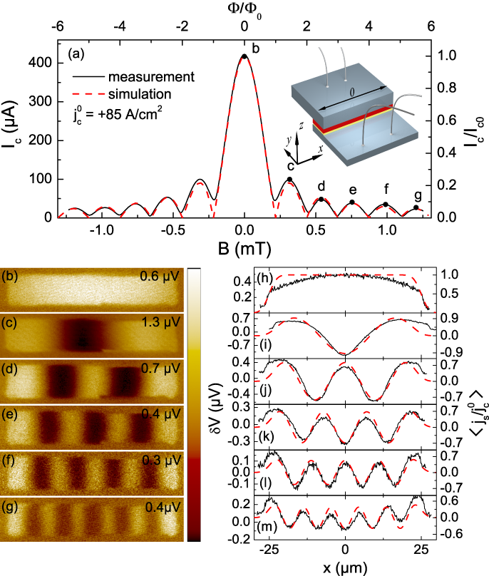
We first discuss results obtained on a 0 junction (#1 in Tab. 1). Fig. 2 shows dependence, LTSEM images and corresponding line scans taken at . The left hand ordinate of Fig. 2(a) gives in physical units while on the right hand ordinate we have normalized to . In the graph we compare to the Fraunhofer dependence, , with . In fact, having more complex structures in mind, rather than using the analytic expression, we have calculated the simulated curve in Fig. 2(a) as
| (18) |
where is a phase ansatz. Unless stated otherwise, we will assume a linear phase ansatz as given by Eq. (5). We note here that for junctions containing both 0 and segments may differ by some in 0 and regionsKemmler et al. (2009); Scharinger et al. (2009). However, for the sake of simplicity, we ignore this effect here.
For the present junction we have used . The resulting calculated curve, shown by the dashed line in Fig. 2(a), agrees with the experimental one, confirming the assumed homogeneity of . From the value of we find and . Thus, the junction is in the short junction limit with , justifying the use of the linear phase ansatz (5). Further, by comparing the abscissas of the experimental and simulated curves, one finds that corresponds to . From this we obtain in good agreement with the value of . Note that due to a magnetic field misalignment there will be a slight out-of-plane field component subject to flux focusing by large area superconducting films Ketchen et al. (1985). This leads to an increased value of calculated using the above procedure.
Fig. 2(b) shows an LTSEM image at . The corresponding line scan is shown by the solid line in Fig.2(h). For one would expect a constant response within the junction area. The actual response is somewhat smaller at the junction edges than in the interior. Taking the finite LTSEM resolution into account, i.e. calculating the convoluted supercurrent density distribution from Eq. (9), one obtains the dashed line which follows the measured response more closely, although there are still differences that may be caused by the junction, either by a parabolic variation of or by a variation in conductance . To test this we implemented a parabolic variation of along in the calculation of and found that the main effect is a slight reduction of the first side minima. To still be consistent with the measured the variation should be well below 10% and is thus most likely not the origin of the variation. To discuss a potential effect we quantify the response using Eq. (13). For the image the bias current was set to 1.05. The function amounts to 0.24 while for we obtain 0.62, i.e. changes in conductance contribute by about 1/3 to the total signal. Thus, variations of in principle could be responsible for the observed variation of . However, while we could accept a simple gradient of along , the bending in which is symmetric with respect to the junction center, is hard to understand. We thus do not have a clear explanation for the parabolic shape of . To quantify the LTSEM response further, we can look at its maximum value . With , from Eq. (13) one estimates and from that a beam-induced temperature change , which is somewhat less than estimated from beam-induced changes.
Fig. 2(c) shows the LTSEM image taken at the first side maximum of . The field-induced sinusoidal variation of can nicely be seen. The corresponding line scan is shown by the solid line in Fig. 2(i) together with , calculated using Eq. (9). Here, a potential parabolic-like variation of , if present, would be overshadowed by the stronger field-induced variation. However, the sinusoidal variation of with an amplitude of around an offset value of points to beam-induced changes in conductance. With the bias current we find and , i.e. we expect a 20% shift of the sinusoidal supercurrent-induced variation of towards lower voltages, roughly in agreement with observation. Further, from the modulation amplitude of and we estimate in agreement with the estimates for the zero field case.
Finally, Figs. 2(d)–(g) show LTSEM images and Figs. 2(j)–(m) corresponding line scans for higher order maxima in . In all cases, the field-induced modulation of can be seen clearly, and simulated curves for , calculated using Eq. (9), are in good agreement with measurements.
We found similar results also for other reference junctions, including ones. In the latter case, typical values at of the critical current densities are (see e.g. #2 in Tab. 1). This value is not large, but it is almost an order of magnitude higher than what has been previously reported for SIFS junctionsWeides et al. (2006a).
III.1.2 0- Josephson junction
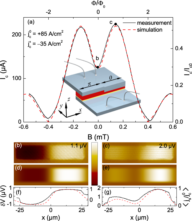
Now we discuss data for a 0- junction (#3 in Tab. 1) presented in Fig. 3. The simulated curve in Fig. 3(a) fits the experimentally measured dependence in the best way for . The right hand axis is normalized to . From the measured value of and the junction area we find and . For a 0- junction, can only be defined in 0 and parts separately, but not for the junction as a whole. However, one can find a normalized junction length as
| (19) |
where and are the total lengths of 0 and parts and and are the Josephson lengths in the 0 and parts, respectively. With this definition we calculate , showing that the junction is again in the short limit. For we obtain a reasonable value of . Further note that the measured is slightly asymmetric, i.e. the main maximum at negative field is slightly lower than at positive field. This effect, which is not reproduced by the simulated curve, is due to the finite magnetization of the F-layer which, in addition, is different in the 0 and parts. This effect is addressed elsewhereKemmler et al. (2009).
For the 0- junction, at =0 the supercurrents of the two halves should have opposite sign. The part giving the smaller contribution to should show inverse flow of supercurrent with respect to the applied bias current, i.e., the part in our case. This can be seen nicely in Fig. 3(b) showing an LTSEM image at zero field. The part is on the left hand side. For comparison, Fig. 3(d) shows a image of the supercurrent density distribution, calculated using Eq. (9). For better comparison, Fig. 3(f) shows a measured and a calculated line scan. The left ordinate is shifted by relative to the origin of the right ordinate to match the simulated and experimental curves. This shift is required to account for the beam-induced conductance change. More quantitatively, with , and assuming that is the same for 0 and parts, we estimate . For the part we estimate , while for the 0 part we obtain . The peak-to-peak voltage modulation in the LTSEM image is . From these numbers we estimate , or , which is reasonable. For the conductance-induced shift we obtain a value of about , which is about a factor of 2 less than expected from the measurement, but still within the error bars.
The LTSEM image shown in Fig. 3(c) has been taken at the main maximum of . Here, both parts of the junction give a positive response. The measurement is in good agreement with expectations, as can be seen in the calculated image in Fig. 3(e) and by comparing the line scans and shown in Fig. 3(g). Note that the “offset problem” seems to be less severe here. Indeed, with and we obtain and for the 0 part and for the part. The supercurrent term thus clearly dominates.
III.1.3 0--0 Josephson junction
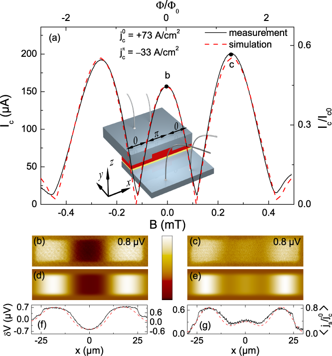
Next we discuss data for a 0--0 junction (#4 in Tab. 1) presented in Fig. 4. The best fit to was obtained for and . From here we obtain(). We are thus again in the short junction limit. Further, we obtain .
LTSEM images, taken at, respectively, the central maximum and the main maximum at positive fields, are shown in Figs. 4(b) and (c). Figs. 4(d) and (e) are simulated images, and Figs. 4(f) and (g) show the corresponding line scans. For this junction, the simulated curves, taking only modulations due to into account, agree well with the data. For Fig. 4(b), with and we find and, for the maximum in the 0 part, . For the maximum in the part we obtain . The offset is thus not very large. From the peak-to-peak modulation of we estimate and, thus, a reasonable value . Taking this value, we estimate the offset voltage to about . For the measurement at the main maximum with we obtain , , and . Using 0.035 K we expect an offset in of and a maximum supercurrent response of 0.85 V in the 0 parts, and 0.3 V in the central part. The measured numbers are 0.65 and 0.35, respectively.
III.1.4 Josephson junction
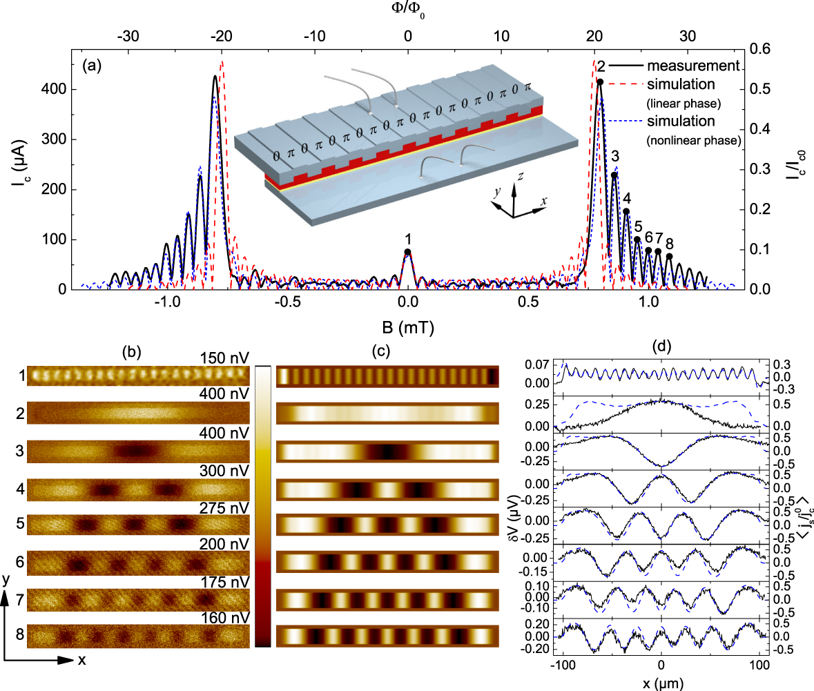
Having seen that well behaving 0--0 junctions can be fabricated one may consider multisegment structures where many 0- segments are joined. The main purpose here is to check the complexity and reliability of the structures that can be fabricated already now. Moreover, as already mentioned in the introduction, multi-segment Josephson junctions are promising for the realization of a junction. The structure we study here has twenty segments (#5 in Tab. 1). In Fig. 5(a) we compare the measured dependence (solid line) with the one calculated (dashed line) using Eq. (18) with a linear phase ansatz (5). However, on both sides of each main peak we see quite substantial deviations of the calculated curve from the experimental one. In particular, the series of maxima following the main peak are much higher in experiment than in simulations based on Eqs. (18) and (5). It is interesting that such a shape of was also measured for -wave/-wave zigzag shaped ramp junctionsSmilde et al. (2002); Ariando et al. (2005); Gürlich et al. (2009).
To understand the origin of such deviations, we have tested numerically a variety of local inhomogeneities in the different facets, ranging from random scattering to gradients and parabolic profiles, always using the linear phase ansatz (5). None of them, and also no variations in effective junction thickness were able to qualitatively reproduce the features described above. Finally, it turned out that the quantity to be modified is the phase ansatz, i.e., the field becomes non-uniform. Adding a cubic term, which accounts for a small phase bending, we have (assuming )
| (20) |
Calculating using Eq. (18) with from Eq. (20), we were able to reproduce the above mentioned features of the experimental dependence, as shown by the dotted line in Fig. 5(a). Here we used , i.e. a rather small correction to the linear phase. In spite of this, for the relatively high magnetic fields around the main maxima of , this term adds up to an additional phase and becomes important — the contribution to the integral in Eq. (18) changes essentially close to the junction ends. Note that a homogeneous junction or a junction consisting of only a few 0 and segments could not sense that, since at the high fields, where the bending of the phase reaches values of at the junction edges, is already suppressed to almost zero.
As we will show in a separate publication Scharinger et al. (2009) the origin of the nonlinear contribution in Eq.(20) is a parasitic magnetic field component perpendicular to the junction plane, which appears due to a misalignment between the plane and the applied magnetic field. This perpendicular component causes screening currents that result in a non-uniform (constant+parabolic) field focused inside the junction and pointing in direction. Similar effects can also be present in non-local planar junctionsMoshe et al. (2009), but we are far from this limit.
By comparing the nonlinear-phase simulation to the measured we infer , and . The junction is thus still in the short limit. We further obtain , which is higher than the value we obtained for the other rectangular structures, but consistent with the fact that we have a focused out-of-plane field component.
Fig. 5(b) shows a series of LTSEM images. Image 1 is taken at , image 2 at the main maximum and images 3 to 8 at the subsequent maxima. For image 1 one can nicely see the modulation induced by the 40 facets, although negative signals are not reached any more. This is due to the small facet size of 5 m which is on the LTSEM resolution limit. At the main maximum the signal is strong and positive, with a slight long-range modulation but no evidence of modulations due to the individual facets any more. At the higher maxima (images 3 to 8) additional minima appear in . Fig. 5(c) shows the corresponding images calculated using the cubic phase ansatz, and Fig. 5(d) shows the corresponding line scans, comparing the measured (solid lines) with the calculated (dotted lines). As can be seen, the agreement is excellent, except for the line scan taken at the maximum. Here, the measured response is strongly weakened towards the junction edges in contrast to the calculated modulation of . For this bias, with we estimate and . It is thus not very likely that the discrepancy is caused by a spatially varying conductance. On the other hand, from the well behaved LTSEM images at zero field we can rule out a long range variation of and as well. A possible origin of this behavior may be a non-uniform field focusing that results in a phase ansatz , which is more complicated than the cubic one of Eq. (20). However, we have to admit that we did not succeed in finding a proper dependence.
We have measured several junctions. All behaved similar to the one discussed here, including the shape of with a well developed set of maxima following the main peak and also with respect to LTSEM images. Thus, the present SIFS technology is fully able to deliberately produce quite complicated multi-facet 0- junctions.
III.2 Disk Shaped and Annular Junctions
III.2.1 Disk shaped Josephson junction
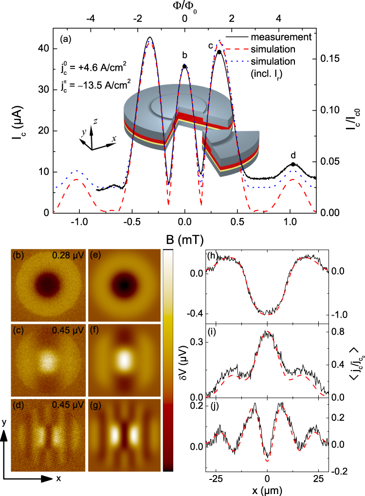
The SIFS technology offers the possibility to create a more complex 0- boundary than a linear one. An intriguing option is to close this boundary in a loop. The disk shaped junction #6 in Tab. 1 is of this type. Here, we use a coordinate system with its origin at the center of the disk, see the inset of Fig. 6(a). The dependence, shown in Fig. 6(a), exhibits a central maximum at where the critical currents of the 0 and the part subtract, as well as prominent side maxima. By fitting the curve calculated using Eq. (18) (dashed line) to the experimental curve (solid line), we obtain and as optimal fitting parameters. Referring to as the junction length we obtain , i.e. again the junction is in the short limit. Fitting the horizontal axis using the length we obtain .
For this sample, (at zero field) is rather low. As a consequence the detectability of at low values of the critical current is resolution limited. We used a voltage criterion to measure the “critical current”, yielding a parasitic background of . When comparing simulation with experiment the value of should be added (in quadrature) to the calculated critical current to obtain the “visible critical current ”, which should be compared with the experimental one , i.e.,
| (21) |
One can see in Fig. 6(a) that the calculated curve including (dotted line) is in good agreement with the experimental data.
Fig. 6(b) shows an LTSEM image taken at the central maximum of . Fig. 6(e) shows the corresponding simulation of and Fig. 6(h) contains corresponding experimental and calculated line scans. The LTSEM data and the simulation results agree well, showing that the supercurrent in the central region flows against the bias current. Figs. 6(c),(f),(i) show the results for an applied magnetic field corresponding to the first side maximum of the curve. Here, the field-induced sinusoidal variation of the supercurrent is superimposed with the disk shaped 0- variation. The supercurrents in the region as well as in a major part of the 0 region flow in the direction of the bias current, maximizing . For completeness, in Figs. 6(d),(g),(j) we also show corresponding plots taken at the second side maximum of . Here, the magnetic field induces about 7 half oscillations of the supercurrent density along . Similar to the previous cases, experimental and calculated plots agree well. For the central maximum with we find and , . Thus, the offset due to conductance changes is minor in this case. The same holds for the other bias points. The main reason is that the factor entering is large (e.g. about 7 for the part at ).
III.2.2 Annular Josephson junction
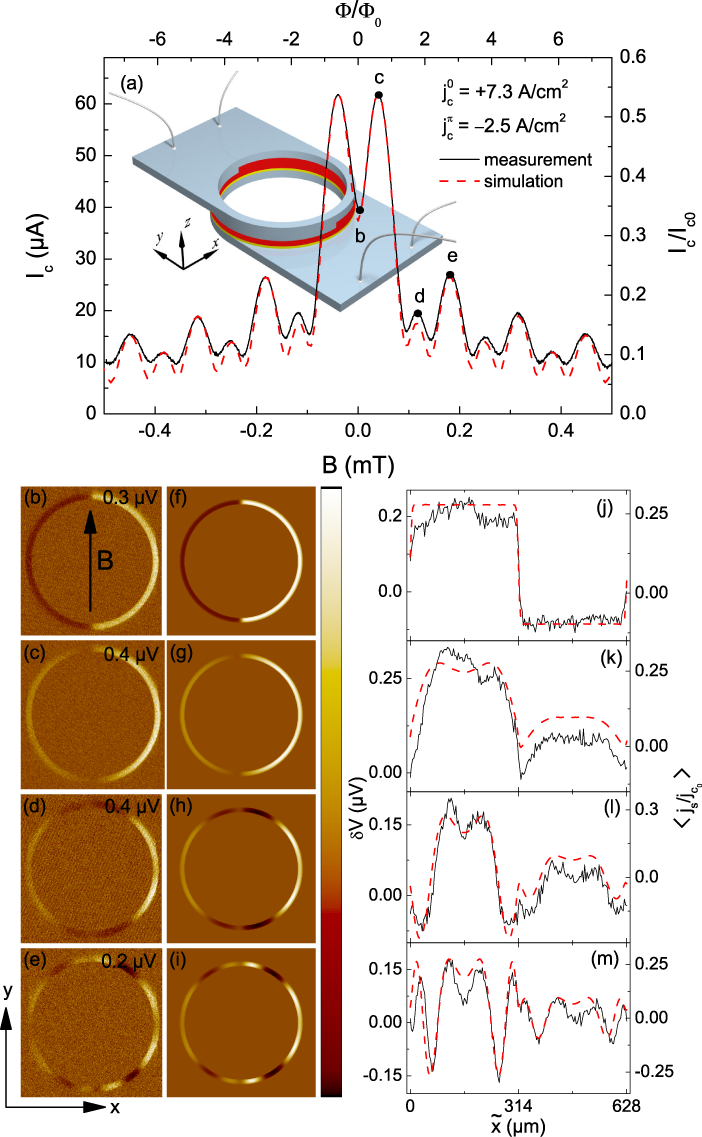
The last structure we want to discuss in this paper is an annular 0- junction (#7 in Tab. 1, see the sketch in Fig. 7). Half of the ring is a 0 region and the other half is a region. One thus obtains an annular junction with two 0- boundaries. If the junction were long in units of it would be a highly interesting object to study (semi)fluxon physics, similar to the case of Nb junctions equipped with injectorsGoldobin et al. (2004); Kienzle et al. (2009). For this junction we use a coordinate system with its origin in the center of the ring, and the steps in the F-layer are located on the axis. Fig. 7(a) shows of this structure, with . The critical current is always above . This offset is in fact real and reproduced by the simulated which is for (the actual value only slightly lifts the minima). From the fit we obtain a ratio . Taking into account that , we get and and, referring to the circumrefence as the junction length, . Thus, we are still in the short junction limit. Further, we obtain , which is somewhat lower than for the other junctions, but still reasonable.
Figures 7(b)–(e) show LTSEM images taken at various values of as labeled in the pattern shown in Fig. 7(a). As shown in Fig. 7(b) for = 0, i.e. at the central local minimum in , a counterflow in the part (left half) can be seen. At the main maximum the supercurrents in both the 0 and the region flow in the direction of bias current [Fig. 7(c)]. Images (d) and (e), taken at the subsequent maxima, look more complicated, showing several regions of counterflow. In all cases, however, the LTSEM images are well reproduced by simulations, as can be seen in Figs. 7(f)–(i) and the corresponding linescans, see Figs. 7(j)–(m). The linescans, taken along the junction circumference, start at the upper 0- boundary and continue clockwise.
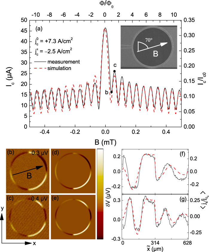
For this annular junction we have also rotated the magnetic field by about 70∘ towards the direction. The corresponding data are shown in Fig. 8. For this field orientation strongly differs from the case , cf., Fig. 8(a), but can be reproduced by simulations, using the same and as in Fig. 7. Furthermore, simulations show that if the field is rotated further towards the axis, the height of the side maxima in decreases, reaching only half of their height of the 70∘ case when the field is parallel to the axis and the minima reach zero. Thus, the annular 0- junction reacts very sensitive to field misalignments relative to the axis, similar to the case of the junction where out-of-plane field components strongly altered . For completeness, Fig. 8(b)–(g) also shows LTSEM images taken at the selected bias points labeled in Fig. 8(a) and compare them with simulation. The agreement is again very good.
IV Conclusion
We have studied a variety of SIFS Josephson junction geometries: rectangular 0, , -, -- and junctions, disk-shaped 0- junction, where the 0- boundary forms a ring, and an annular junction with two 0- boundaries. Using LTSEM we were able to image the supercurrent flow in these junctions and we demonstrate that 0 and parts work as predicted having and . Within each 0 or part, according to both LTSEM images and , the critical current density is rather homogeneous. Particularly, within our experimental resolution of a few , we saw no inhomogeneities that might have been caused by an inhomogeneous magnetization of the F-layer. This implies that ferromagnetic domains, although probably present, must have a size well below .
These results demonstrate the capabilities of the state-of-the-art SIFS technology. Arrangements like the ring-shaped 0- boundary are impossible to realize using other known 0- junction technologiesSmilde et al. (2002); Hilgenkamp et al. (2003); Ariando et al. (2005); Goldobin et al. (2004). Even intersecting 0- boundaries seem to be feasible, e.g., by arranging 0 and segments in a checkerboard pattern.
For the regions we demonstrated a record value of at , which is an order of magnitude higher than the values previously reported for SIFS junctions with a NiCu F-layer Weides et al. (2006a, b). Still, to obtain reasonable values of , should be increased by at least one order of magnitude to reach . Then the 0- junctions can be made long enough (in units of ) to study the dynamics of semifluxons pinned at the 0- boundaries. In this case semifluxon shapes, not realizable with other types of junctions, are possible, e.g., closed loops, intersecting vortices, etc.. Another issue inherent to the present SIFS technology is that the critical current densities and in the 0 and parts are not identical in general. In many cases this does not matter, e.g., when one works with semifluxons in a long junction. If is required, the difference in and will lead to a low yield of the circuit and one is perhaps restricted to operate the device in a narrow temperature interval, where and are closer to each other.
Even with the present restrictions, quite complex geometries like the junctions have been realized. Those SIFS multifacet junctions already showed interesting features, like their high sensitivity to nonuniform magnetic fields, and they will be usable for many fundamental studies, e.g. on the way of realizing junctions.
Acknowledgements.
We gratefully acknowledge financial support by the Deutsche Forschungsgemeinschaft via SFB/TRR-21 and project WE 4359/1-1, and by the German Israeli Foundation via research grant G-967-126.14/2007.References
- Bulaevski et al. (1977) L. N. Bulaevski, V. V. Kuzi, and A. A. Sobyanin, JETP Lett. 25, 290 (1977).
- Terzioglu et al. (1997) E. Terzioglu, D. Gupta, and M. R. Beasley, IEEE Trans. Appl. Supercond. 7, 3642 (1997).
- Terzioglu and Beasley (1998) E. Terzioglu and M. R. Beasley, IEEE Trans. Appl. Supercond. 8, 48 (1998).
- Ustinov and Kaplunenko (2003) A. V. Ustinov and V. K. Kaplunenko, J. Appl. Phys. 94, 5405 (2003).
- Ortlepp et al. (2006) T. Ortlepp, Ariando, O. Mielke, C. J. M. Verwijs, K. F. K. Foo, H. Rogalla, F. H. Uhlmann, and H. Hilgenkamp, Science 312, 1495 (2006).
- Ioffe et al. (1999) L. B. Ioffe, V. B. Geshkenbein, M. V. Feigel’man, A. L. Fauchre, and G. Blatter, Nature (London) 398, 679 (1999).
- Blatter et al. (2001) G. Blatter, V. B. Geshkenbein, and L. B. Ioffe, Phys. Rev. B 63, 174511 (2001).
- Yamashita et al. (2005) T. Yamashita, K. Tanikawa, S. Takahashi, and S. Maekawa, Phys. Rev. Lett. 95, 097001 (2005).
- Yamashita et al. (2006) T. Yamashita, S. Takahashi, and S. Maekawa, Appl. Phys. Lett. 88, 132501 (2006).
- Ryazanov et al. (2001) V. V. Ryazanov, V. A. Oboznov, A. Y. Rusanov, A. V. Veretennikov, A. A. Golubov, and J. Aarts, Phys. Rev. Lett. 86, 2427 (2001).
- Kontos et al. (2002) T. Kontos, M. Aprili, J. Lesueur, F. Genet, B. Stephanidis, and R. Boursier, Phys. Rev. Lett. 89, 137007 (2002).
- Blum et al. (2002) Y. Blum, A. Tsukernik, M. Karpovski, and A. Palevski, Phys. Rev. Lett. 89, 187004 (2002).
- Bauer et al. (2004) A. Bauer, J. Bentner, M. Aprili, M. L. Della-Rocca, M. Reinwald, W. Wegscheider, and C. Strunk, Phys. Rev. Lett. 92, 217001 (2004).
- Sellier et al. (2004) H. Sellier, C. Baraduc, F. Lefloch, and R. Calemczuk, Phys. Rev. Lett. 92, 257005 (2004).
- Oboznov et al. (2006) V. A. Oboznov, V. V. Bol ginov, A. K. Feofanov, V. V. Ryazanov, and A. I. Buzdin, Phys. Rev. Lett. 96, 197003 (2006).
- Weides et al. (2006a) M. Weides, M. Kemmler, E. Goldobin, D. Koelle, R. Kleiner, H. Kohlstedt, and A. Buzdin, Appl. Phys. Lett. 89, 122511 (2006a).
- Vavra et al. (2006) O. Vavra, S. Gazi, D. S. Golubovic, I. Vavra, J. Derer, J. Verbeeck, G. VanTendeloo, and V. V. Moshchalkov, Phys. Rev. B. 74, 020502(R) (2006).
- Bannykh et al. (2009) A. A. Bannykh, J. Pfeiffer, V. S. Stolyarov, I. E. Batov, V. V. Ryazanov, and M.Weides, Phys. Rev. B. 79, 054501 (2009).
- van Dam et al. (2006) J. A. van Dam, Y. V. Nazarov, E. P. A. M. Bakkers, S. D. Franceschi, and L. P. Kouwenhoven, Nature (London) 442, 667 (2006).
- Cleuziou et al. (2006) J.-P. Cleuziou, W. Wernsdorfer, V. Bouchiat, T. Ondarcuhu, and M. Monthioux, Nature Nanotech. 1, 53 (2006).
- Jorgensen et al. (2007) H. Jorgensen, T. Novotny, K. Grove-Rasmussen, K. Flensberg, and P. Lindelof, Nano Lett. 7, 2441 (2007).
- Baselmans et al. (1999) J. J. A. Baselmans, A. F. Morpurgo, B. J. V. Wees, and T. M. Klapwijk, Nature (London) 397, 43 (1999).
- Baselmans et al. (2002) J. J. A. Baselmans, B. J. van Wees, and T. M. Klapwijk, Phys. Rev. B 65, 224513 (2002).
- Huang et al. (2002) J. Huang, F. Pierre, T. T. Heikkilä, F. K. Wilhelm, and N. O. Birge, Phys. Rev. B 66, 020507(R) (2002).
- Bulaevski et al. (1978) L. N. Bulaevski, V. V. Kuzi, and A. A. Sobyanin, Solid State Commun. 25, 1053 (1978).
- Xu et al. (1995) J. H. Xu, J. H. Miller, and C. S. Ting, Phys. Rev. B. 51, 11958 (1995).
- Goldobin et al. (2002) E. Goldobin, D. Koelle, and R. Kleiner, Phys. Rev. B 66, 100508(R) (2002).
- Kirtley et al. (1996) J. R. Kirtley, C. C. Tsuei, M. Rupp, J. Z. Sun, L. S. Yu-Jahnes, A. Gupta, M. B. Ketchen, K. A. Moler, and M. Bhushan, Phys. Rev. Lett. 76, 1336 (1996).
- Kirtley et al. (1999) J. R. Kirtley, C. C. Tsuei, and K. A. Moler, Science 285, 1373 (1999).
- Hilgenkamp et al. (2003) H. Hilgenkamp, Ariando, H. H. Smilde, D. H. A. Blank, G. Rijnders, H. Rogalla, J. Kirtley, and C. C. Tsuei, Nature (London) 422, 50 (2003).
- Weides et al. (2006b) M. Weides, M. Kemmler, H. Kohlstedt, R. Waser, D. Koelle, R. Kleiner, and E. Goldobin, Phys. Rev. Lett. 97, 247001 (2006b).
- Smilde et al. (2002) H.-J. H. Smilde, Ariando, D. H. A. Blank, G. J. Gerritsma, H. Hilgenkamp, and H. Rogalla, Phys. Rev. Lett. 88, 057004 (2002).
- Ariando et al. (2005) Ariando, D. Darminto, H. J. H. Smilde, V. Leca, D. H. A. Blank, H. Rogalla, and H. Hilgenkamp, Phys. Rev. Lett. 94, 167001 (2005).
- Gürlich et al. (2009) C. Gürlich, E. Goldobin, R. Straub, D. Doenitz, Ariando, H.-J. H. Smilde, H. Hilgenkamp, R. Kleiner, and D. Koelle, Phys. Rev. Lett. 103, 067011 (2009).
- Mannhart et al. (1996) J. Mannhart, H. Hilgenkamp, B. Mayer, C. Gerber, J. R. Kirtley, K. A. Moler, and M. Sigrist, Phys. Rev. Lett. 77, 2782 (1996).
- Buzdin and Koshelev (2003) A. Buzdin and A. E. Koshelev, Phys. Rev. B. 67, 220504(R) (2003).
- Goldobin et al. (2007) E. Goldobin, D. Koelle, R. Kleiner, and A. Buzdin, Phys. Rev. B 76, 224523 (2007).
- Mints (1998) R. G. Mints, Phys. Rev. B 57, R3221 (1998).
- Mints and Papiashvili (2001) R. G. Mints and I. Papiashvili, Phys. Rev. B 64, 134501 (2001).
- Mints et al. (2002) R. G. Mints, I. Papiashvili, J. R. Kirtley, H. Hilgenkamp, G. Hammerl, and J. Mannhart, Phys. Rev. Lett. 89, 067004 (2002).
- Gross and Koelle (1994) R. Gross and D. Koelle, Rep. Prog. Phys. 57, 651 (1994).
- Weides et al. (2007) M. Weides, C. Schindler, and H. Kohlstedt, J. Appl. Phys. 101, 063902 (2007).
- Chang and Scalapino (1984) J. J. Chang and D. J. Scalapino, Phys. Rev. B. 29, 2843 (1984).
- Chang et al. (1985) J. J. Chang, C. H. Ho, and D. J. Scalapino, Phys. Rev. B. 31, 5826 (1985).
- Stewart (1968) W. C. Stewart, Appl. Phys. Lett. 12, 277 (1968).
- McCumber (1968) D. McCumber, J. Appl. Phys. 39, 3113 (1968).
- (47) The color scale of all images is symmetric around zero, with the maximum values given on each image.
- Kemmler et al. (2009) M. Kemmler, M. Weides, M. Weiler, T. B. Goennenwein, A. S. Vasenko, A. A. Golubov, H. Kohlstedt, D. Koelle, R. Kleiner, and E. Goldobin, arXiv:0910.5907 (2009).
- Scharinger et al. (2009) S. Scharinger, C. Gürlich, M. Weides, R. G. Mints, H. Kohlstedt, D. Koelle, R. Kleiner, and E. Goldobin, unpublished (2009).
- Ketchen et al. (1985) M. B. Ketchen, W. J. Gallagher, A. W. Kleinsasser, S. M. S, and J. R. Clem, Proc. SQUID 85, Superconducting Quantum Interference Devices and their Applications ed. H. D. Hahlbohm and H. Lübbig (Berlin: Walter de Gruyter) p. 865 (1985).
- Moshe et al. (2009) M. Moshe, V. G. Kogan, and R. G. Mints, Phys. Rev. B. 79, 024505 (2009).
- Goldobin et al. (2004) E. Goldobin, A. Sterck, T. Gaber, D. Koelle, and R. Kleiner, Phys. Rev. Lett. 92, 057005 (2004).
- Kienzle et al. (2009) U. Kienzle, T. Gaber, K. Buckenmaier, K. Ilin, M. Siegel, D. Koelle, R. Kleiner, and E. Goldobin, Phys. Rev. B. 80, 014504 (2009).