,
Is keV ion induced pattern formation on Si(001) caused by metal impurities?
Abstract
We present ion beam erosion experiments performed in ultra high vacuum using a differentially pumped ion source and taking care that the ion beam hits the Si(001) sample only. Under these conditions no ion beam patterns form on Si for angles with respect to the global surface normal using 2 keV Kr+ and fluences of . In fact, the ion beam induces a smoothening of preformed patterns. Simultaneous sputter deposition of stainless steel in this angular range creates a variety of patterns, similar to those previously ascribed to clean ion beam induced destabilization of the surface profile. Only for grazing incidence with pronounced ion beam patterns form. It appears that the angular dependent stability of Si(001) against pattern formation under clean ion beam erosion conditions is related to the angular dependence of the sputtering yield, and not primarily to a curvature dependent yield as invoked frequently in continuum theory models.
pacs:
81.16.Rf, 81.65.Cf, 68.49.Sf, 81.15.Jj, 87.64.DzKeywords: Si(100), silicon, surface, krypton, Kr, ion beam, pattern formation, co-deposition, STM, nanoholes, nanodot, nanoripples, smoothening, impurities, Fe, iron
1 Introduction
Ion beam surface patterning of amorphous and crystalline materials has attracted considerable interest in the recent years. This interest is of twofold origin. First it results from the intricate physics involved in ion beam patterning which has not yet been entirely uncovered. Second, ion beam nanopatterning is a relatively cheap and low tech method with a number of potential applications ranging from an anti-reflection surface finish [1, 2, 3] over orienting large molecules [4] to nanomagnetism [5, 6, 7, 8]. As Si is a prime material of technology and readily available in high purity and quality, it is not surprising that the ion beam patterning studies are numerous for Si. At room temperature Si readily amorphizes during ion exposure [9]. The loss of anisotropy and crystal structure appeared to make it an ideal material to be described by the continuum theory of ion erosion, which effectively averages out atomistic details of the processes. Early theoretical work in the continuum theory approximation considered the dependence of the sputtering yield on the angle of the ion beam with the respect to the local surface normal as a decisive factor for surface morphological evolution ([10, 11] and references therein). Note that we distinguish here and in the following between the local angle of incidence (measured with respect to the surface normal of a specific surface element) and the global angle of incidence (measured with respect to the normal of the average surface plane). Since the seminal publication of Bradley and Harper [12] the dependence of the sputtering on surface curvature was considered to be the key for pattern formation. While there are certain conditions, where ion beam erosion of Si does not cause pattern formation [13, 14], the overwhelming number of investigations find pattern formation on Si in a large parameter space. One class of prototypical patterns are dot or hole patterns observed for normal incidence noble gas ion erosion with energies up to a few keV and at temperatures in the amorphization regime [14, 15, 16, 17, 18, 19]. Another class of exemplary patterns are ripple ones with the ripple wave vector parallel to the ion beam azimuth. Quite some observations here refer to elevated temperatures in the crystalline regime [20, 21, 22]. However, also at room temperature in the amorphous regime ripple patterns were observed [23, 24, 25, 26], the most regular ones for slight off-normal conditions with using noble gas ions with energies up to a few keV [14, 27, 28, 29]. The variety and complexity of observed patterns stimulated the development of continuum theories [30, 31, 32, 33, 34] extending the concept of the curvature dependent yield as prime destabilization mechanism.
Co-deposition of trace amounts of foreign species during ion erosion has been found already long time ago to give rise to microstructure formation [35, 36, 37, 38]. It is currently used as a tool for surface texturing [39, 40]. Recently it became obvious that impurities may influence pattern formation unintentionally. Mo co-sputtered from sample clips during ion erosion was found to foster dot formation at normal incidence [41, 42, 43]. The ion flux and fluence were found to affect the amount of Mo and Fe deposited on the sample from the ion source and thereby to change normal incidence patterns [44, 45].
In this situation the question arises, whether there is a hidden chemical or impurity factor in pattern formation on Si. Such a largely disregarded attribute could make it impossible for theory to come up with an adequate material parameter based description of pattern formation. We therefore conducted an erosion study under clean surface science conditions, using ion beam parameters for which we expected pattern formation to take place.
2 Experimental
The experiments were performed in a variable temperature scanning tunneling microscopy (STM) apparatus [46] with a base pressure mbar equipped with a differentially pumped ion source, a low energy electron diffraction (LEED) system, and a load-lock for Si sample transfer. For erosion the samples were exposed to a 2 keV Kr+ fine focus ion beam with full width at half maximum mm scanned over a sample area of about 4 mm 4 mm resulting in a time averaged ion flux of at 300 K at angles . The fluence was . Due to differential pumping during ion exposure the working pressure was below mbar. The ion current onto the sample was controlled with a Faraday cup, which could be moved precisely into the sample position. After ion exposure the pressure dropped quickly into the mbar range and imaging by STM was performed subsequently. For the co-sputter deposition experiments a piece of target material was mounted vertically on the sample. The ion beam was impinging at onto the sample surface and with an angle onto the sputter target. In the co-sputter deposition experiments the fluence was only , but still sufficient to guarantee pattern development. Again the samples were analyzed in situ by STM and subsequently analyzed ex situ by atomic force microscopy (AFM), secondary electron microscopy (SEM), a compact phase-shifting interferometer and secondary ion mass spectrometry (SIMS). For SIMS we used 250 eV O for depth profiling. Quantitative image analysis was conducted by WSxM [47] and differential sputter yield and energy distribution calculations were performed with TRIM.SP [48].
3 Angle dependent smoothening and pattern formation on Si(001)
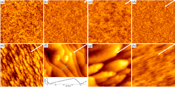
The -dependence of the morphology after ion bombardment is shown in Fig. 1. Unexpectedly, for no patterns form and the root mean square roughness remains very low, nm [compare Figs. 1(a) - 1(d)]. For as shown in Fig. 1(e) ripples with a small amplitude and wave vector parallel to the ion beam azimuth developed. From the power spectral density of large topographs we obtain an average wavelength of nm. Still the surface does not destabilize to any significant extent: is just nm after removal of the order of of material. Pronounced pattern formation takes place in a narrow angular range , just around the angular range of maximum sputter yield . At represented by Fig. 1(f) we find a pronounced sawtooth profile ripple pattern with nm. The sawtooth profile displays extended facets forming a small angle of with respect to the global surface plane resulting in an angle of the ion beam with respect to the local surface normal [compare inset of 1(f)]. The smaller facets form an apparent angle of with respect to the surface plane, resulting in an apparent angle of the ion beam with respect to the local surface normal. Due to convolution of the surface profile with the STM tip of finite sharpness the apparent is just an upper bound to the true angle of the ion beam with respect to the local surface normal, which is likely to be much lower. At represented by Fig. 1(g) instead of ripples we find roof tile structures [40]. The structures are now elongated along the ion beam and if one would like to assign a to them (which is not justified), it would now be normal rather than parallel to the ion beam azimuth. The roughness is with nm similar to the case. Note also that the facet structure of the roof tiles in Fig. 1(g) has similarities, but also discrepancies compared to Fig. 1(f). Also the roof tiles display extended facets parallel to the ion beam direction with a small angle with respect to the global surface plane resulting in . The facets normal to the ion beam direction visible in Fig. 1(f) became arrow tips. The angle of the arrow tips with respect to the average surface plane is limited again by the surface profile – tip convolution. In Fig. 1(h) for the surface is extremely smooth again with nm. A faint ripple pattern with normal to the ion beam azimuth is visible; however, the amplitude of the pattern is marginal. If forced to define a critical angle of ripple rotation we would set it to , in reasonable agreement with previous work [40] finding a for 5 keV Xe+ ion erosion of Si.
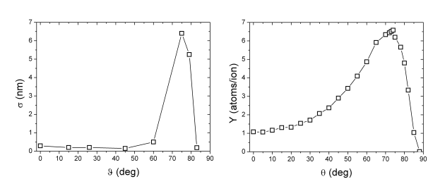
Figure 2(a) summarizes the evolution of already discussed during the presentation of the STM data above. The absence of roughening for is no accident, but due to an inherent smoothening action of the ion beam. To support this idea after STM imaging of the rough ripple pattern with nm, we exposed it to a fluence of of 4 keV Kr+ at normal incidence () and halved thereby the roughness.
In order to discuss the mechanism of pattern formation for we consider the angular dependence of the sputter yield on the local angle of incidence as calculated by TRIM.SP and shown in Fig. 2(b). Evidently, this distinction is only relevant, when the surface is not flat. displays a broad local minimum for , an absolute minimum for with and a strong maximum around (see also [49]). It is obvious, that pronounced patterns develop only for global angles of incidence close to the maximum of , i.e. where the erosion rate is largest and where the erosion rate depends strongly on . This points to the application of the deterministic approach of erosion profile evolution, where the sputtering yield is assumed to be a function only of the local surface gradient [50, 51, 10, 11].
If the sputter yield depends only on the local angle of incidence , a smooth surface eroded under a global angle can become unstable, if fluctuations are present which give rise to locally varying sputtering yields. An analysis of surface topography evolution assuming that the sputter yield only depends on the local incidence angle shows that, due to fluctuations, an initially flat surface can decompose into a faceted profile which displays facets where the sputter yield is a minimum or maximum [50, 51]. For these facets which predominate during ion erosion the local ion incidence angles are given by , , or , respectively. It should be noted, that facets can only form if in the initial surface profile ion incidence angles are already existing [50, 52]. For surfaces with small height fluctuation this condition is only achieved if is close to .
As the average surface orientation is maintained during erosion, in the angular range the surface profile decomposes into patches with local ion impingement angles close to the minima of , i. e. into facets and with . Considering the example represented by Fig. 1(f) with the flat surface decomposes into a sawtooth profile with facets forming a large angle with the ion beam and facets nearly parallel to the ion beam (). For both and the yield is much smaller than for [compare Fig. 2(b)]. It is evident that such a sawtooth profile considerably reduces the global erosion rate. However, the observed local angles and do not match the theoretical predictions of and . For the steep facet we attribute this difference largely to inability of our STM tip to measure the proper angle. For the facet with the small slope the difference of the measured and predicted can not rely on a measurement problem. The measured difference may have the following reasons: (i) The fluence used was too low to allow the surface to reach the dynamic equilibrium and the ensuing facets; (ii) There is a significant uncertainty in the TRIM.SP calculations of for very grazing angles due to the fast change of the yield with and its sensitive dependence on surface structure. The yield at might thus be already close to zero, such that the driving force (minimization of erosion rate) has largely vanished and a further change of the facet angle is kinetically frozen.
In contrast, for near normal ion incidence angles , and surfaces with small height fluctuations are stable because profiles with are steady state surface configurations [50, 51]. Furthermore, as hillocks are eroded faster than valleys (contrary to the Bradley-Harper theory [12]) the ion beam induces a smoothening of rough surfaces in this angular range as observed by us experimentally (compare also Fig. 4 of [11] and [53]).
For the case of room temperature ion beam erosion of Si with 2 keV Kr+, the angular dependence of appears to explain the ranges of stability observed as well as the orientation of the pattern facets formed in the unstable regime. So far we left open, which kind of fluctuations might initiate the faceting of the surface for . While the stochasticity of the ion impacts gives rise to fluctuations by itself, it may be that other effects contribute to fluctuations, e.g. a curvature dependence of the sputtering yield. However, the pattern formation scenario we observe here can hardly be reconciled with models based on Bradley-Harper theory. A curvature dependent yield as destabilization mechanism neither explains the extended angular range of stability nor the rather abrupt angle-dependent transitions from smooth surfaces to faceted patterns and back to smooth surfaces, i.e. abrupt transitions from surfaces with zero curvature to ones with curvature singularities. By invoking the angular dependence of to explain surface destabilization, no predictions related to time scales necessary for pattern evolution nor to characteristic length scales in the pattern are possible. We therefore consider the angular dependence of only as one important element in a theory of pattern formation on Si. Secondary effects - e.g. surface diffusion, ballistic drift, viscous flow, etc. - must probably be considered to be responsible for selection of characteristic scales.
With ion energies of the order of 1 keV and for noble gases like Ar+, Kr+ or Xe+ and angles a large variety of dot and ripple patterns was obtained by us [14, 27, 28, 29] and other groups [15, 16, 17, 18, 23]. We consider these results to be at variance with the present findings. It was noticed recently that the relative concentrations of Mo and Fe emerging from the ion source during sputtering influence the pattern appearance at [44, 45]. However, whether patterns evolve at all without impurities was not considered. Our observations are consistent with the observation of Mo-seeding at [41, 42, 43] and the absence of patterns without Mo-seeding [41, 42]. We claim here that patterns are entirely absent without intentional or unintentional co-deposition of impurities after noble gas bombardment on Si(001) with energies of the order of 1 keV and for . Below we provide additional evidence for this statement.
4 Angle dependent pattern formation on Si(001) with co-sputter deposition
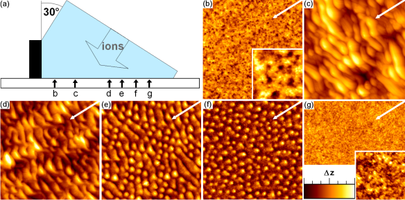
To substantiate our claim that impurities resulting from the sputtering process are in fact responsible for the great number of patterns resulting for ion erosion with we performed dedicated co-sputter deposition experiments. As sketched in Fig. 3(a) the ion beam was impinging at onto the sample surface, i. e. at an angle where no pattern formation is expected. Additionally the ion beam hits a piece of stainless steel (Fe 84% and Cr 13%) at an angle , from which some material is sputter deposited onto the eroding Si surface. This setup is similar to the arrangement used for surfactant sputtering [40]. The STM topographs were taken along a line normal to the center of the steel plate. As obvious from Figs. 3(b)-(g) the resulting morphologies strongly depend on the normal distance to the stainless steel plate. Fig. 3(b) displays a relatively smooth surface with small hole structures as highlighted by the inset (compare also [44]). With increasing the roughness shoots up beyond 10 nm and ripples with parallel to the ion beam azimuth form [compare Figs. 3(c) and (d)]. Upon further increase of the roughness decreases again and the ripple pattern transforms [Fig. 3(e)] to a dot pattern [Fig. 3(f)]. Eventually, for the largest distance measured is comparable to a situation without co-sputter deposition and patterns are absent [compare insets of Figs. 3(b) and (g)].
Not every co-sputtered material induces patterns. We used the same set-up with a plate of highly oriented pyrolytic graphite instead of stainless steel. The entire Si wafer remained smooth with a roughness nm and no patterns formed.
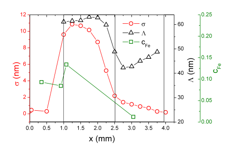
Figure 4 displays the roughness (open dots, left -axis), the feature separation (open triangles, right inner -axis) and the Fe concentration (open squares, right outer -axis) for the patterns on the Si wafer as function of . Schematically, four pattern ranges are distinguished in Fig. 4: nanoholes with , ripples with , dots with and a smooth surface for . The roughness displays a pronounced maximum in the ripple range with nm, fades gradually away in the dot range with nm and is very low in the nanohole and smooth surface range with nm. The characteristic feature separation varies unspectacularly from a typical ripple wavelength nm to a typical dot separation with nm. Based on the variety of patterns we expected an inhomogeneous Fe concentration . As Rutherford backscattering needs a much larger sample spot (a few mm) for chemical analysis, we decided to perform secondary ion mass spectrometry. Quantification of our data is based on the tables of SIMS impurity signals in Si obtained for 8 keV O sputtering [54, 55]. Here we used 250 eV O to mimimize implantation and mixing and achieve a high depth resolution. The surface roughness and the potentially inhomogeneous Fe distribution makes our quantification problematic, which therefore should be considered with caution. We measure a maximum of the relative iron concentration in the ripple range. Still is sufficient to induce the dot range. It appears plausible that due to ion beam induced mixing the co-sputtered Fe forms a silicide in the surface near layers as it has been found for normal incidence ion bombardment through an alternating cold cathode ion source [44].
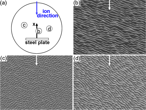
We further explored the pattern at locations displaced from the normal to the center of the stainless steel plate (i.e. left and right of the x-axis) by scanning electron microscopy. Figure 5(a) sketches the locations of the SEM micrographs displayed in Fig.5(b)-(d). It is obvious that the ripple wave vector depends on the position with respect to the stainless steel plate. Apparently is parallel to the average azimuthal direction of the atoms sputter deposited from the stainless steel plate onto the Si wafer.
The co-sputter situation is complex and in order to prepare an understanding of pattern formation in this situation it is mandatory to consider energy, direction and species of the particles impinging onto the Si wafer. A given location on the Si wafer in front of the stainless steel plate receives 2 keV Kr+ ions, sputtered Fe atoms (we neglect Cr atoms in the following discussion for simplicity) and Kr particles reflected from the stainless plate. Fig. 6(a) displays the differential Fe sputter yield averaged over the azimuthal angular range as calculated by TRIM.SP [48]. The distribution of the Fe atoms is anisotropic with a broad peak of emission centered at about . As the Si wafer can be imagined horizontally under the polar diagram, the main flux of sputtered Fe atoms is directed towards the Si wafer. The total yield per 2 keV Kr+ is substantial and amounts to .
Fig. 6(b) shows the differential backscattering coefficient of the Kr+ particles backscattered from the stainless steel plate and averaged over the azimuthal angular range . The distribution of the backscattered particles is peaked at an exit angle of . In average the backscattered Kr particles will hit the Si wafer closer to the stainless steel plate than the sputtered Fe atoms, i.e. at a smaller distance . The total backscattering coefficient amounts to .
Fig. 6(c) displays the energies of the sputtered Fe atoms and of the backscattered Kr particles as a function of the polar emission angle . The data plotted is averaged over the azimuthal angular range . The energy of the sputtered Fe atoms is moderate with a maximum of eV for . Note that at the most probable angle of emission of sputtered Fe atoms the energy of the sputtered Fe atoms is only about eV in the presented azimuthal angular range. The average energy of the Fe atoms sputtered in the azimuthal angular range is eV, the average energy of all atoms sputtered in forward direction with is eV. Though substantial, the energy of the Fe particles is insufficient to cause significant sputtering of the Si wafer. The energy of the backscattered Kr particles increases monotonically with their emission angle and reaches eV for . Note that at the most probable emission angle of the energy of the emitted particles is about 755 eV. The backscattered particles will therefore cause strong erosion of the Si wafer near the steel plate. The average energy of the backscattered Kr particles in the presented azimuthal angular range is eV, the average energy of all particles backscattered towards the Si plate in the angular range is eV.
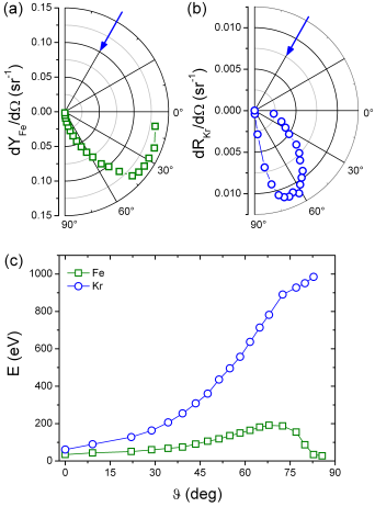
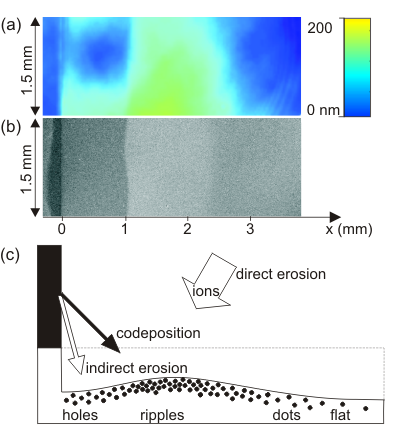
Fig. 7(a) displays a section of a height topograph of the Si-wafer after co-sputter deposition measured by phase-shifting interferometry. We attribute the hill in the height profile in the range with a height of nm to the significant amount of co-sputtered Fe in this range. Note that the hill does not consist entirely of Fe - actually most of the co-sputter deposited Fe has been resputtered by the Kr+ ion beam. However, the co-sputter deposited Fe partly shielded the Si from being removed by the direct Kr+ ion beam resulting in a significantly reduced erosion depth. The trough next to the stainless steel plate for results from the additional sputtering caused by the energetic component of the Kr particles reflected from the stainless steel plate. According to mirco phase interference patterns at the edge of the scanning area of the ion beam the average erosion depth is nm. The SEM topograph in Fig. 7(b) shows a contrast change at the onset of the co-sputter hill caused by the transition from the smooth nanohole to the rippled surface. This is also consistent with the pattern sequence as observed by STM in Fig. 4. In view of the significant flux and energy of the reflected Kr particles arriving in the trough area, there the lower is a consequence of the enhanced resputtering. Dot patterns form beyond the co-sputter deposition hill, where the arriving flux of Fe atoms is lower resulting in a lower . Fig. 7(c) summarizes the discussion schematically and displays the link between the arriving particles, the erosion depth and the patterns formed.
Based on the data the three following conclusions are obtained. (i) Dot patterns form during 2 keV Kr+ ion beam erosion with for moderate co-sputtered Fe concentrations and in the absence of reflected Kr particles, i.e. in the absence of a second component of energetic particles impinging from a different direction onto the substrate. (ii) Ripple patterns form on the Si substrate for high co-sputtered Fe concentrations: As the flux and the energy of the reflected Kr particles arriving in the ripple pattern area are small, their presence appears not to be necessary for ripple pattern formation. However Fig. 5 proves that the direction of impingement of the co-sputtered Fe atoms determines the orientation of the ripple wave vector . Whether ripple orientation towards the stainless steel plate is due to the additional directed energy of the arriving Fe particles or due to the directed attachment of the Fe particles to elevations (ripple slopes) in their line of sight can not be resolved by the present experiment. (iii) Erosion by the direct beam together with strong sputtering from a different direction (here through the reflected energetic Kr particles) prevents formation of a pronounced and rough pattern. Although we detect a significant amount of Fe for , the area remains rather smooth and the nanohole pattern is neither pronounced nor well ordered.
As a global key result of our experiments we consider the fact that supply of a second chemical species is mandatory for pattern formation on Si in a large parameter range, specifically for . Whether co-sputter deposition must be considered also for pattern formation of other materials or other energy ranges outside the 1 keV region as a hidden parameter remains to be investigated. To obtain a deeper understanding beyond this point and to disentangle the effects of a second chemical species and of additional energy from a second direction (at variance with the primary ion beam direction) dedicated experiments are necessary. It would be useful to design a situation where the second chemical species is deposited with thermal energies (e.g. through physical vapor deposition) simultaneously with a clean eroding ion beam. Such an experiment might also be able to establish whether the direction of the impinging co-deposited particles with respect to the ion beam and the sample surface is of relevance - irrespective of the energy of the co-deposited particles. As pattern formation is always the result of the interplay of a destabilizing mechanism and a stabilizing or smoothening one, the nature of the latter needs to be explored as well. We suggest to perform co-sputter deposition or co-evaporation experiments at very low ( K) or elevated temperatures K to test the relevance of thermal diffusion.
We believe that our experiments are relevant for future theoretical work. After the decade of continuum theory evolution there appears now to be a need for (i) a material parameter based description of pattern formation; (ii) for a theory that takes into account the absence of pattern formation for a large parameter space; (iii) a model which includes the effect of impurities for an explanation of pattern formation.
5 Conclusions
Room temperature ion beam erosion of Si through 2 keV Kr+ shows no pattern formation for . For rough ion beam faceted ripple and roof tile patterns are formed. It is speculated that patterns observed for are the result of unintentional co-sputter deposition of metallic impurities resulting from the use of broad beam ion sources with a divergent beam. The angular ranges of stability and instability as well as the observed faceting can be understood on the basis of the -dependence of the sputtering yield.
Intentional co-sputter deposition of stainless steel from a plate hit together with the Si sample by the ion beam leads to a complex sequence of patterns in dependence of the distance from steel plate. These patterns form at angles , where no patterns result for clean ion erosion. Nano hole, ripple and dot patterns are formed. Nano hole patterns are observed under the influence of strong additional sputtering by ions reflected from the steel plate and of co-sputtered steel. Ripple and dot patterns are formed in a distance range where reflected ions are largely absent. The ripple wave vector of the ripple patterns is found to be aligned to the direction of the impinging steel atoms. The formation of ripple and dot patterns is distinguished by the concentration of co-sputtered material. Dots contain much less co-sputtered material than ripples.
We believe that our results are relevant for future research in ion beam pattern formation on Si. They will foster additional experimental work to uncover the mechanisms of pattern formation due to the simultaneous deposition of a second chemical species. They also point to the need for well controlled erosion experiments and chemical analysis of the eroded surfaces to rule out impurity effects. Lastly, we hope they stimulate theoretical work, reconsidering the effect of the slope dependent sputtering yield for pattern formation and investigating the effects of impurities on pattern formation.
References
References
- [1] Wilson S J and Hutley M C 1982 Optica Acta 29 993
- [2] Flamm D, Frost F and Hirsch D 2001 Appl. Surf. Sci. 179 95
- [3] Fouckhardt H, Steingoetter I, Brinkmann M, Hagemann M, Zarschizky H and Zschiedrich L 2007 Advances in OptoElectronics Article ID 27316 1
- [4] Chaudhari P, Lacey J, Doyle J, Galligan E, Lien S C A, Callegari A, Hougham G, N D Lang P S A, John R, Yang K H, Lu M H, Cai C, Speidell J, Purushothaman S, Ritsko J, Samant M, Stohr J, Nakagawa Y, Katoh Y, Saitoh Y, Sakai K, Satoh H, Odahara S, Nakano H, Nakagaki J and Shiota Y 2001 Nature 411 56
- [5] Zhang K, Rotter F, Uhrmacher M, Ronning C, Krauser J and Hofsäss H 2007 New J. Phys. 9 29
- [6] Zhang K, Uhrmacher M, Hofsäss H and Krauser J 2008 J. Appl. Phys. 103 083507
- [7] Liedke M O, Liedke B, Keller A, Hillebrands B, Mücklich A, Facsko S and Fassbender J 2007 Phys. Rev. B: Condens. Matter 75 220407
- [8] Teichert C, de Miguel J J and Bobek T 2009 J. Phys. Condens. Matter 21 224025
- [9] Kótai E 1994 Nucl. Instrum. Methods Phys. Res., Sect. B 85 588
- [10] Katardjiev I V, Carter G and Nobes M J 1989 Vacuum 39 1069
- [11] Carter G 2001 J. Phys. D: Appl. Phys. 34 R1
- [12] Bradley R M and Harper J M E 1988 J. Vac. Sci. Technol., A 6 2390
- [13] Madi C S, Davidovitch B, George H B, Norris S A, Brenner M P and Aziz M J 2008 Phys. Rev. Lett. 101 246102
- [14] Ziberi B, Cornejo M, Frost F and Rauschenbach B 2009 J. Phys. Condens. Matter 21 224003
- [15] Gago R, Vázquez L, Cuerno R, Varela M, Ballesteros C and Albella J M 2001 Appl. Phys. Lett. 78 3316
- [16] Gago R, Vázquez L, Plantevin O, Sánchez-García J A, Varela M, Ballesteros M C, Albella J M and Metzger T H 2006 Phys. Rev. B: Condens. Matter 73 155414
- [17] Fan W B, Li W Q, Qi L J, Sun H T, Luo J, Zhao Y Y and Lu M 2005 Nanotechnology 16 1526
- [18] Fan W B, Ling L, Qi L J, Li W Q, Sun H T, Gu C X, Zhao Y Y and Lu M 2006 J. Phys. Condens. Matter 18 3367
- [19] Ziberi B, Frost F, Rauschenbach B and Höche T 2005 Appl. Phys. Lett. 87 033113
- [20] Erlebacher J, Aziz M J, Chason E, Sinclair M B and Floro J A 1999 Phys. Rev. Lett. 82 2330
- [21] Erlebacher J, Aziz M J, Chason E, Sinclair M B and Floro J A 2000 Phys. Rev. Lett. 18 5800
- [22] Brown A D and Erlebacher J 2005 Phys. Rev. B: Condens. Matter 72 075350
- [23] Gago R, Vázquez L, Cuerno R, Varela M, Ballesteros C and Albella J M 2002 Nanotechnology 13 304
- [24] Habenicht S, Lieb K P, Koch J and Wieck A D 2002 Phys. Rev. B: Condens. Matter 65 115327
- [25] Keller A, Facsko S and Möller W 2008 New J. Phys. 10 063004
- [26] Keller A, Cuerno R, Facsko S and Möller W 2009 Phys. Rev. B: Condens. Matter 79 115437
- [27] Ziberi B, Frost F, Höche T and Rauschenbach B 2005 Phys. Rev. B: Condens. Matter 72 235310
- [28] Ziberi B, Frost F, Höche T and Rauschenbach B 2006 Vacuum 81 155
- [29] Ziberi B, Frost F and Rauschenbach B 2006 J. Vac. Sci. Technol., A 24 1344
- [30] Makeev M A, Cuerno R and Barabási A L 2002 Nucl. Instrum. Methods Phys. Res., Sect. B 197 185
- [31] Facsko S, Bobek T, Stahl A and Kurz H 2004 Phys. Rev. B: Condens. Matter 69 153412
- [32] Castro M, Cuerno R, Vázquez L and Gago R 2005 Phys. Rev. Lett. 94 016102
- [33] Vogel S and Linz S J 2007 Phys. Rev. B: Condens. Matter 75 085425
- [34] Chan W L and Chason E 2007 J. Appl. Phys. 101 121301
- [35] Wehner G K and Hajicek D J 1971 J. Appl. Phys. 42 1145
- [36] Punzel J and Hauffe W 1972 Phys. Status Solidi A 14 K97
- [37] Robinson R S and Rossnagel S M 1982 J. Vac. Sci. Technol. 21 790
- [38] Rossnagel S M and Robinson R S 1982 J. Vac. Sci. Technol. 20 195
- [39] Tanemura M, Yamauchi H, Yamane Y, Ohita T and Tanemura S 2004 Nucl. Instrum. Methods Phys. Res., Sect. B 215 137
- [40] Zhang K, Hofsäss H, Rotter F, Uhrmacher M, Ronning C and Krauser J 2009 Surf. Coat. Technol. 203 2395
- [41] Ozaydin G, Öczan A S, Wang Y, Ludwig K F, Zhou H, Headrick R L and Siddons D P 2005 Appl. Phys. Lett. 87 163104
- [42] Ozaydin-Ince G and Ludwig Jr K F 2009 J. Phys. Condens. Matter 21 224008
- [43] Teichert C, Hofer C and Hlawacek G 2006 Adv. Eng. Mater. 8 1057
- [44] Sánchez-García J A, Vázquez L, Gago R, Redondo-Cubero A, Albella J M and Czigány Z 2008 Nanotechnology 19 224009
- [45] Sánchez-García J A, Gago R, Caillard R, Redondo-Cubero A, Martin-Gago J A, Palomares F J, Fernández M and Vázquez L 2009 J. Phys. Condens. Matter 21 224009
- [46] Polop C, Rosiepen C, Bleikamp S, Drese R, Mayer J, Dimyati A and Michely T 2007 New J. Phys. 9 1
- [47] Horcas I, Fernández R, Gómez-Rodríguez J M, Colchero J, Gómez-Herrero J and Baro A M 2007 Rev. Sci. Instrum. 78 013705
- [48] Eckstein W 1994 Radiat. Eff. Defects Solids 130 239
- [49] Ducommun J P, Cantagrel M and Moulin M 1975 J. Mater. Sci. 10 52
- [50] Carter G, Colligon J S and Nobes M J 1973 J. Mat. Sci. 8 1473
- [51] Carter G, Colligon J S and Nobes M J 1977 Radiat. Eff. Defects Solids 31 65
- [52] Wei Q, Lian J, Boatner L A, Wang L M and Ewing R C 2009 Phys. Rev. B: Condens. Matter 80 085413
- [53] Carter G, Nobes M J and Katardjiev I V 1992 Philos. Mag. B 66 419
- [54] Stevie F A and Wilson R G 1991 J. Vac. Sci. Technol., A 9 3064
- [55] Wilson R G 1995 Int. J. Mass Spectrom. Ion Processes 143 43