Microscopic theory of absorption and emission in nanostructured solar
cells:
Beyond the generalized Planck formula
Abstract
Absorption and emission in inorganic bipolar solar cells based on low dimensional structures exhibiting the effects of quantum confinement is investigated in the framework of a comprehensive microscopic theory of the optical and electronic degrees of freedom of the photovoltaic system. In a quantum-statistical treatment based on non-equilibrium Green’s functions, the optical transition rates are related to the conservation of electronic currents, providing a quantum version of the balance equations describing the operation of a photovoltaic device. The generalized Planck law used for the determination of emission from an excited semiconductor in quasi-equilibrium is replaced by an expression of extended validity, where no assumptions on the distribution of electrons and photons are made. The theory is illustrated by the numerical simulation of single quantum well diodes at the radiative limit.
pacs:
72.20.Jv, 72.40.+w,73.21.Fg, 73.40.Kp, 78.67.DeI Introduction
Knowledge about the luminescence of solar cells is of great value both for the characterization of the cell and for the analysis of the device performance due to its correspondence to the radiative losses. Established theories predicting the luminescent emission of bulk solar cells are mainly based on the generalized Planck and Kirchhoff formulas [wuerfel:82, ] relating the emitted photon flux to the absorptivity and the bias voltage. However, the generalized Planck spectrum was derived based on the crucial assumption that the carriers are well described by a local equilibrium distribution characterized by a single quasi-Fermi level and at the temperature of the lattice. This assumption is no longer justified in nanostructured solar cells based on quantum wells or quantum dots [tsui:96, ; nelson:97, ; bremner:99, ; barnham:00, ; kluftinger:00, ; kluftinger:01, ; honsberg:02, ; mazzer:06, ; fuehrer:06, ; fuehrer:07, ]. The purpose of the present work thus is to provide a more general approach to absorption and emission in bipolar semiconductor nanostructures where the critical assumptions are relaxed. To meet the requirements formulated above, a description of emission is derived within a general microscopic nonequilibrium theory of quantum-confined photovoltaic systems [ae:prb_08, ]. The appeal of the approach lies in the way the optical properties of a semiconductor nanostructure are related to its electronic properties on very general grounds. Based on non-equilibrium quantum-statistical mechanics and starting from a quantum theory of electrons and photons in semiconductors nanostructures, absorption and emission are calculated from the transverse polarization function, which appears as the convolution of the non-equilibrium Green’s functions for electrons and holes [kadanoff:62, ; keldysh:65, ; henneberger:96, ; pereira:96, ; pereira:98, ; faleev:02, ; shtinkov:04, ; richter:08, ; henneberger:09, ]. Unlike more basic approaches, the theory allows the inclusion of many-particle corrections and interaction effects, such as those due to electron-phonon coupling or exciton formation.
II Theory
The following outline of the general theory of quantum photovoltaic devices is restricted to the radiative limit, i.e. non-radiative recombination (Shockley-Read-Hall, Auger) and generation (impact ionization) processes are not considered.
II.1 Hamiltonian
At the radiative limit, the full quantum photovoltaic device is described in terms of the model Hamiltonian
| (1) | |||||
| (2) | |||||
| (3) |
consisting of the coupled systems of electrons (), photons () and phonons (). Since the focus is on the electronic device characteristics, only is considered here, however including all of the terms corresponding to coupling to the bosonic systems. Within the electronic part, contains the kinetic energy, the (bulk) band structure and band offsets, and it also includes the electrostatic potential from the solution of Poisson’s equation. The interaction part consists of the terms , and for the interactions of electrons with photons, phonons and electrons or holes, respectively. While the first term describes generation and recombination of free charge carriers via the absorption and emission of photons, the second one provides the carrier relaxation via the absorption and emission of phonons. The last term contains the carrier-carrier interactions responsible for screening effects or exciton formation.
Within the non-equilibrium Green’s function theory of quantum optics and transport in excited semiconductor nanostructures, physical quantities are expressed in terms of quantum statistical ensemble averages of single particle operators, namely the fermion field operator for the charge carriers, the quantized photon field vector potential for the photons and the ionic displacement field for the phonons. The corresponding Green’s functions are
| (4) | |||||
| (5) | |||||
| (6) |
where denotes the contour ordered operator average peculiar to non-equilibrium quantum statistical mechanics [kadanoff:62, ; keldysh:65, ] for arguments with temporal components on the Keldysh contour [keldysh:65, ].
II.2 Dyson’s equations
The Green’s functions follow as the solutions to corresponding Dyson’s equations [pereira:96, ; pereira:98, ; schaefer:02, ],
| (7) | ||||
| (8) | ||||
| (9) |
, and are the propagators for noninteracting electrons, photons and phonons, respectively, denotes tensorial transverse quantities and labels the phonon mode. The electronic self-energy encodes the renormalization of the charge carrier Green’s functions due to the interactions with photons and phonons, i.e. generation, recombination and relaxation processes. Charge injection and absorption at contacts is considered via an additional boundary self-energy term reflecting the openness of the system. The photon and phonon self-energies and describe the renormalization of the optical and vibrational modes, leading to phenomena such as photon recycling or the phonon bottleneck responsible for hot carrier effects.
II.3 Microscopic optoelectronic conservation laws
The macroscopic equation of motion for a photovoltaic system is the continuity equation for charge carriers,
| (10) |
where and are particle and current density respectively, the generation rate and the recombination rate of carriers species . The corresponding microscopic conservation law reads [kadanoff:62, ]
| (11) |
In steady state, the continuity equation (10) is reduced to
| (12) |
In the microscopic theory, the divergence of the current corresponds to the ””-component of the RHS in (11)
| (13) |
If the energy integration is restricted to one carrier species, the above equation corresponds to the microscopic version of (12), and expresses the total local radiative interband transition rate. The total radiative interband current is found by integrating the divergence over the absorbing/emitting volume, and is equivalent to the total global transition rate, and, via the Gauss theorem, to the difference of the current at the boundaries of the absorbing/emitting region. On the other hand, the global radiative rate equals the total optical rate , related to the global electromagnetic energy dissipation through
| (14) |
and which, via the quantum statistical average of the Poynting vector operator, can be expressed in terms of photon Green’s functions and self-energies [richter:08, ; henneberger:09, ], providing the following microscopic expressions for absorbed and emitted photon flux
| (15) | ||||
| (16) | ||||
| (17) |
where the photon density of states
| (18) |
was introduced. The expression for replaces the generalized Kirchhoff formula [wuerfel:82, ] for the photon flux emitted from an excited semiconductor. It allows for the inclusion of a realistic electronic dispersion via the polarization function , reflecting the effects of electron-electron, electron-hole and electron-phonon interactions and the non-equilibrium occupation of these states, as well as the consideration of the optical modes specific to the geometry of the system.
III Implementation
The general theory outlined above is implemented for quantum well layers inserted in the intrinsic region of a -- diode. Details of this implementation can be found in [ae:prb_08, ]. As a first approximation, the charge carriers are treated as a system interacting with a specified equilibrium environment of photons and phonons, i.e. only the electronic Green’s functions are renormalized. The main aspects of the model for charge carriers, photons and phonons are given below.
III.1 Charge carriers
Electrons and holes are modelled within the framework of empirical tight-binding theory for layered semiconductor heterostructures, where the carrier field operators are expanded in planar orbitals representing linear combinations of Bloch sums of localized atomic orbitals over the plane of periodicity. Interactions among carriers are considered only on the Hartree level, equivalent to the solution of the macroscopic Poisson equation for the effective potential. Inclusion of screening and excitonic effects would require the calculation of two-particle quantities in higher order perturbation theory.
Carrier selective contacts are obtained by applying closed system boundary conditions at minority carrier contacts, which results in a complete supression of leakage currents.
III.2 Photons
Light is described via free field modes with occupation determined by the combination of the spectra of the external illumination and the black-body thermal equilibrium with the environment. For practical computations, the absorption and stimulated emission due to the latter can be neglected. The self-energy in the electronic Dyson equation describing the coupling to charge carriers is computed within perturbation theory on the level of a self-consistent first Born approximation (SCBA) to second order in the electron-photon interaction.
III.3 Phonons
Lattice vibrations are implemented within the harmonic approximation and for noninteracting acoustic as well as polar optical modes. The interaction with the electronic system is on the level of a coupling to an equilibrium heat bath and is described by the corresponding SCBA self-energy.
III.4 Absorption, emission and photon flux balance
The linear absorption coefficient is related to the transverse polarization function or photon self-energy via
| (19) | ||||
| (20) |
where is the background dielectric constant. For dipole coupling to free field photons, the self-energy reads
| (21) |
where describes the dipolar matter-field coupling and the trace is over both layer and orbital indices. For the considered model, the total radiative rate is given by
| (22) |
where is the model layer width. From this representation of the rate follows the intuitive result that the absorbed flux is proportional to the incoming photon flux , while the emitted flux only depends on the polarization .
IV Numerical results
IV.1 Models system: geometry and simulation parameters
The simulated system consists of an ultrathin (∼50 nm) -- diode with a single quantum well embedded in the -region. A two band tight-binding model is used for the electronic structure with the the two bulk band gaps given by =0.6 eV and =0.9 eV, with a symmetric offset of =0.15 eV. The effective masses and the parameters for the electron phonon-interaction are chosen for a GaAs/AlGaAs material system. The system is illuminated at a photon energy of 0.7 eV and an intensity of 1 kW/m2.
IV.2 Local density of states, absorption and emission
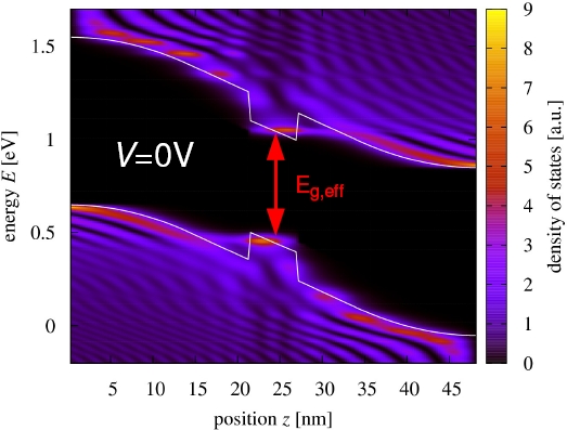
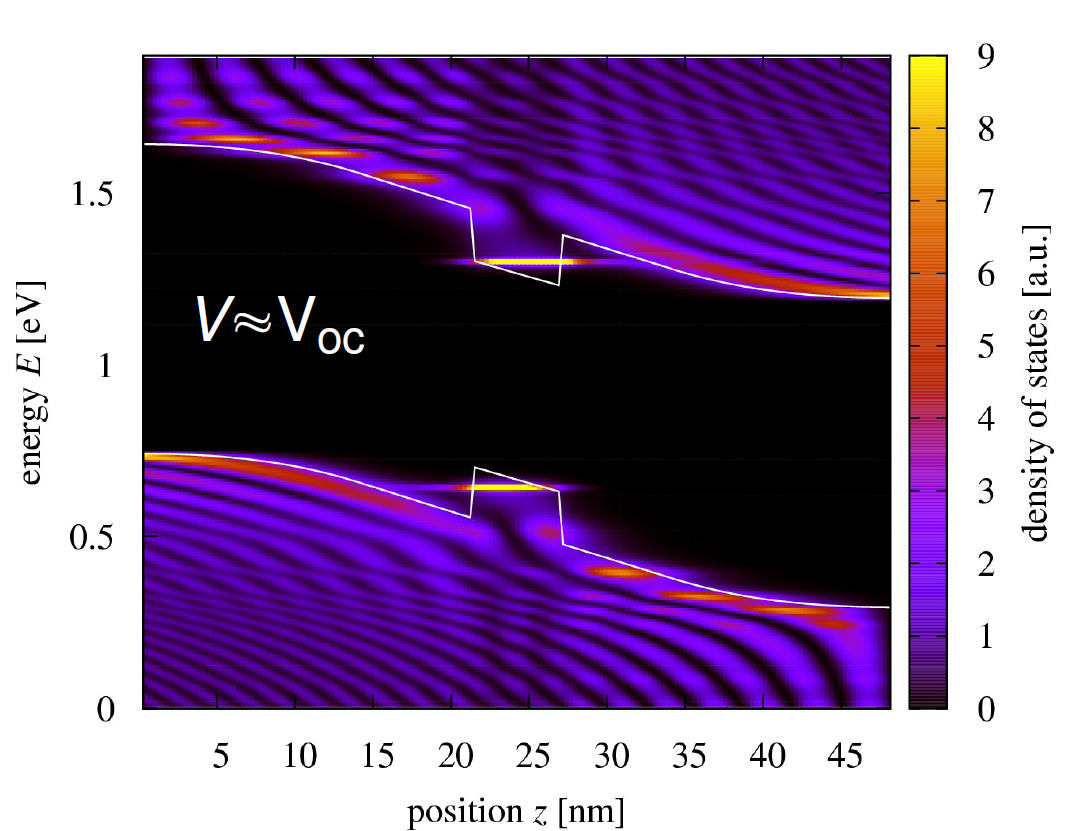
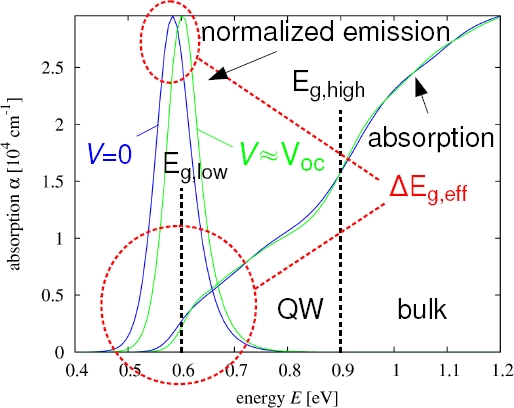
Insertion of a quantum well in the -region of a -- diode locally extends the density of states below the high band gap bulk edge, red-shifting the effective absorption edge, which is now given by the position of the lowest confinement level, as can be seen in Fig. 1 showing the local density of states at zero bias. Under very high fields, as in the case considered, the quantum well states hybridize with the bulk continuum outside the well. The resulting significant deviation from the 2D-DOS is reflected in the absorption, shown in Fig. 3. This so called Franz-Keldysh effect includes an additional red-shift in the effective band edge, which decreases with the effective field at the quantum well location under the application of an external bias voltage and resulting in a blue-shift of the emission edge as the voltage increases from V to V , which is displayed in Fig. 2.
IV.3 Local radiative interband rates
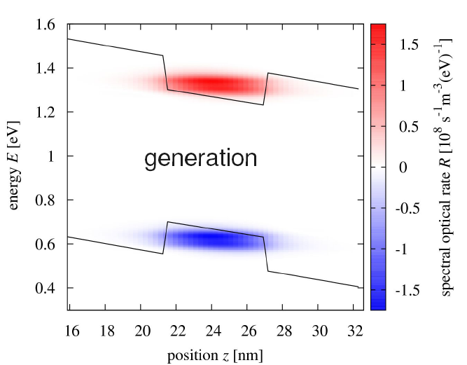
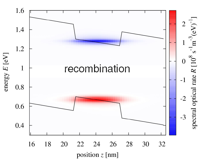
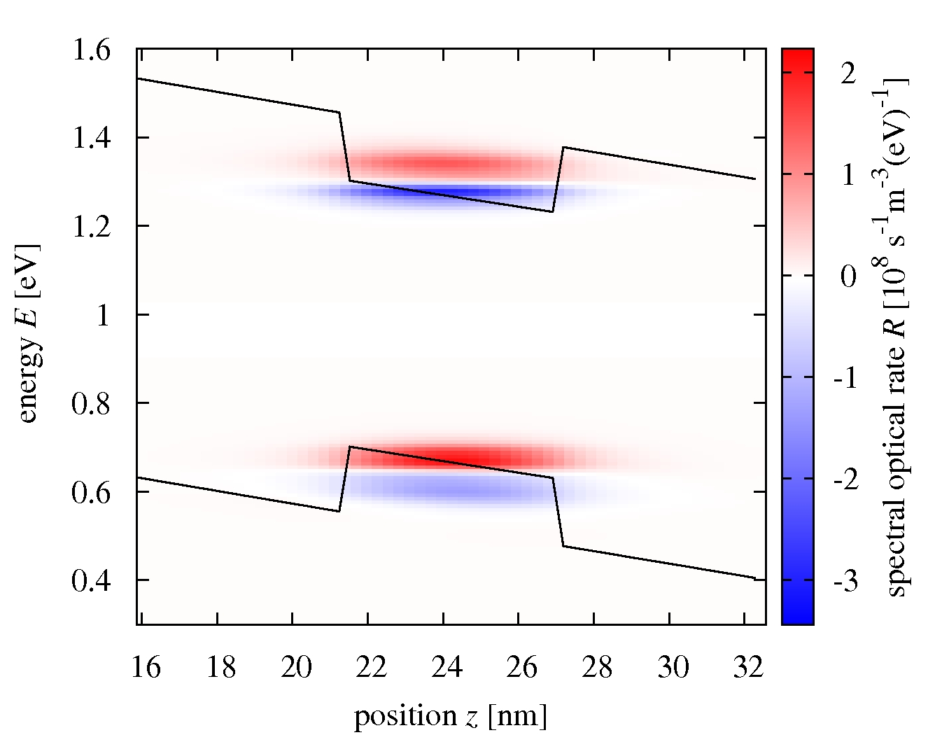
Fig. 4 shows the local interband rates for generation, recombination and the sum of the two effects, as computed via the electronic Green’s functions and self-energies, consisting of inscattering (=generation) and outscattering (=recombination) components. At illumination photon energies exceeding the effective band gap but below the higher bulk gap, net generation and recombination are spectrally well separated and spatially confined to the quantum well, i.e. the region of finite overlap of absorbing electronic and hole quantum well states. On the other hand, integration over energy provides net interband current of the entire device.
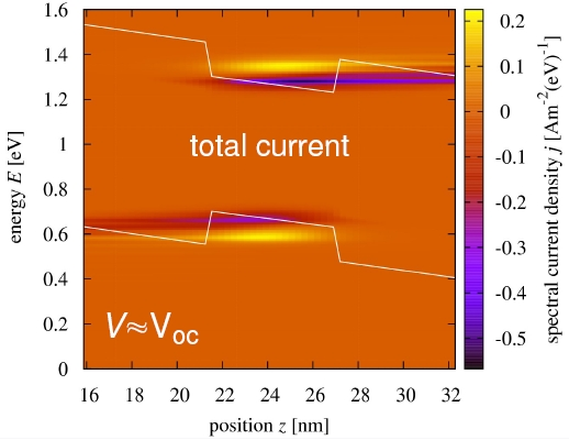
IV.4 Local current spectrum
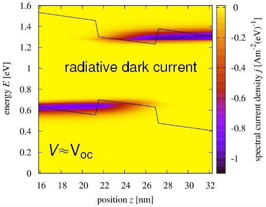
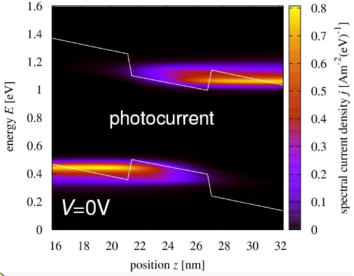
The spectral difference in generation and recombination rates leads to a spatial inhomogeneity in the generation and recombination currents, as seen in Fig. 5, with localization of the maximum in the quantum well, even though the integrated current is locally conserved, and the separate contributions of radiative dark and photocurrent grow towards the contacts and reach their maximum outside the absorbing region.
V Conclusions
Quantum effects in low dimensional nanostructured absorbers for high efficiency solar cells require new approaches for the modelling of absorption and luminescence. A comprehensive microscopic theory of quantum photovoltaic devices including the effects of quantum confinement on the optical, electronic and vibrational properties can be formulated based on the non-equilibrium Green’s functions theory of excited semiconductor nanostructures. Within this theory, microscopic electronic and optical conservation laws are derived and interrelated. Numerical simulations based on an implementation of the theory for quantum well pin-diodes provide a picture resolved in space and energy of the generation, recombination and the corresponding currents in quantum well absorbers at the radiative limit and for both short circuit and close to open circuit conditions.
References
- (1) P. Würfel, J. Phys. C: Solid State Phys. 15, 3967 (1982).
- (2) E. Tsui, J. Nelson, K. Barnham, C. Button, and J. S. Roberts, J. Appl. Phys. 80, 4599 (1996).
- (3) J. Nelson et al., J. Appl. Phys. 82, 6240 (1997).
- (4) S. Bremner, R. Corkish, and C. Honsberg, IEEE Trans. Electron Devices 46, 1932 (1999).
- (5) K. W. J. Barnham et al., J. Mater. Sci.: Mater. Electron. 11, 531 (2000).
- (6) B. Kluftinger, K. Barnham, J. Nelson, T. Foxon, and T. Cheng, Microelectron. Eng. 51-52, 265 (2000).
- (7) B. Kluftinger, K. Barnham, J. Nelson, T. Foxon, and T. Cheng, Sol. Energy Mater. Sol. Cells 66, 501 (2001).
- (8) C. Honsberg, S. Bremner, and R. Corkish, Physica E 14, 136 (2002).
- (9) M. Mazzer et al., Thin Solid Films 511, 76 (2006).
- (10) M. F. Führer et al., Quasi Fermi Level Splitting and Evidence for Hot Carrier Effects in Strain-Balanced Quantum Well Concentrator Solar Cells at High Bias, in Proc. 21st European Photovoltaic Specialists Conference, Dresden, 2006.
- (11) M. F. Führer et al., Quantitative study of hot carrier effects observed in strain-balanced quantum well solar cells, in Proc. 22nd European Photovoltaic Solar Energy Conference, Milan, Italy, 2007.
- (12) U. Aeberhard and R. Morf, Phys. Rev. B 77, 125343 (2008).
- (13) L. P. Kadanoff and G. Baym, Quantum Statistical Mechanics, Benjamin, Reading, MA, 1962.
- (14) L. Keldysh, Sov. Phys.-JETP. 20, 1018 (1965).
- (15) K. Henneberger and S. W. Koch, Phys. Rev. Lett. 76, 1820 (1996).
- (16) M. Pereira and K. Henneberger, Phys. Rev. B 53, 16485 (1996).
- (17) M. Pereira and K. Henneberger, Phys. Rev. B 58, 2064 (1998).
- (18) S. V. Faleev and M. I. Stockman, Phys. Rev. B 66, 085318 (2002).
- (19) N. Shtinkov and S. Vlaev, Phys. Status Solidi B 241, R11 (2004).
- (20) F. Richter, M. Florian, and K. Henneberger, Physical Review B (Condensed Matter and Materials Physics) 78, 205114 (2008).
- (21) K. Henneberger, Phys. Status Solidi B 246, 283 (2009).
- (22) W. Schäfer and M. Wegener, Semiconductor Optics and Transport Phenomena, Springer, 2002.