Coherent transport of armchair graphene constrictions
Abstract
The coherent transport properties of armchair graphene nanoconstrictions(GNC) are studied using tight-binding approach and Green’s function method. We find a non-bonding state at zero Fermi energy which results in a zero conductance valley, when a single vacancy locates at of a perfect metallic armchair graphene nanoribbon(aGNR). However, the non-bonding state doesn’t exist when a vacancy locates at y=3n, and the conductance behavior of lowest conducting channel will not be affected by the vacancy. For the square-shaped armchair GNC consisting of three metallic aGNR segments, resonant tunneling behavior is observed in the single channel energy region. We find that the presence of localized edge state locating at the zigzag boundary can affect the resonant tunneling severely. A simplified one dimensional model is put forward at last, which explains the resonant tunneling behavior of armchair GNC very well.
I Introduction
Owing to many good properties, such as the ultra high Fermi velocity(), the stability due to the sp2 hybridization and the feasibility of large-scale integration, graphene has been regarded as a promising candidate material for post-silicon electronics, and has stirred intensive studiesNovoselov ; Wallace ; Geim1 ; Kim1 ; Castro ; Katsnelson ; Fujita ; Nakada ; Wakabayashi ; Peres ; Brey ; T.C.Li . Many graphene microstructures have been studied both theoretically and experimentally for future applications, such as the field-effect transistors, the p-n junctions, metallic-metallic(semiconducting) nanojunctions, L-shaped, Z-shaped, T-shaped and cross shaped junctionsObradovic ; Q.Yan ; Liang ; Williams ; Abanin ; SQF ; J.Li ; S.Hong ; Yisong ; Y.P.Chen ; Z.F.Wang ; Z.P.Xu ; Thushari ; JYY ; Yanyang ; Areshkin .
Graphene nanoconstrictions(GNC) is one of the important building blocks for the carbon based electronic circuitsRojas ; A.Rycerz ; Barbaros ; Chuvilin ; Darancet ; Andriotis ; Todd ; Molitor ; Rojas1 . With the combination of etching and deposition techniques, a complete turn off of electrical transport of GNC has been demonstrated as a function of the local gate voltage experimentallyBarbaros . Furthermore, stable and rigid carbon atomic chains were experimentally realized by removing carbon atoms row by row from graphene, which shows the sophisticated technique to control the shape of graphene nanodevicesChuanhong . Theoretical researches mainly focus on two types of GNCs, i.e., the type based on zigzag graphene nanoribbon(zGNR), and the other type based on armchair graphene nanoribbon(aGNR). The wedge-shaped GNCs based on zGNR show a gap in the transmission spectrums, and the zero conductance is related to the appearance of localized zero energy edge statesRojas . Based on a zigzag edged GNC, valley filter is proposed which can produce a valley polarized current. Two valley filters in series may function as an electrostatically controlled valley valveA.Rycerz . As for the GNCs based on aGNR, performance limits of GNR field-effect transistors are investigated by studying a GNC with two semiconducting wide aGNRs attached to a narrow semiconducting oneRojas1 .
In this paper, we first discuss the lattice vacancy effects on the transport properties of metallic aGNR. We then study the coherent transport properties of GNCs with two wide metallic aGNRs attached to a narrow metallic one with two vertical zigzag boundaries(ZBs). We investigate the role of the ZBs of GNCs in the coherent transport by breaking the ZBs one by one. Using a one dimensional model for the GNCs, we are able to understand the resonant tunneling behaviors of the GNCs. Throughout the paper, we use the nearest tight-binding approach and the recursive Green’s function method to analyze the transmission rate and the local density of states(LDOS)Sancho ; Leonor ; Datta ; T.C.Li .
II Single lattice vacancy effect on metallic aGNR
In the nearest tight-binding model, a perfect zGNR is always metallic because of the finite overlap of the two edge statesWakabayashi1 . However, aGNR can be either metallic (for ) or semiconducting (otherwise), where is the width of of aGNR counted by the number of dimmer lines in the transverse direction with an integerPeres . It has been shown that a single vacancy at the edge of aGNR would induce a zero conductance dip in the conductance spectrumT.C.Li . It has also been found that an on-site defect at different positions of aGNR induce different conductance spectrumsJYY . It is then interesting to investigate the transport property in the presence of a single vacancy at various positions of aGNR.
The tight-binding Hamitonian of the aGNR is given by
| (1) |
where is the on-site energy of atom , () the creation(annihilation) operator at site , and the hopping constant between the nearest neighbors.
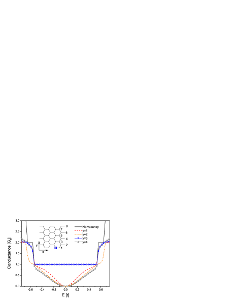
A lattice vacancy can be described by a very large on-site energy in the tight-binding model L.Chico ; Wakabayashi2 . Due to the translational invariance of a perfect aGNR in the axis, we only have to consider the effect of position of the vacancy along the axis. Here we choose the width as an example, see Fig. 1. The vacancy is marked by a square. With the consideration of symmetry along the axis, we only have to consider the vacancy at the four positions, i.e. , , , and .
The conductance spectrums are shown in Fig. 1. The solid line is the conductance spectrum for a perfect aGNR, which shows quantized conductance plateaus. The dashed line, dash dotted line, and solid line with solid spheres represent the cases that a single vacancy resides at , , and . All the three lines show a conductance valley with a zero conductance at . The solid line with open circles shows the conductance spectrum when a single vacancy locates at . We see that the conductance spectrum maintains perfectly the first quantized conduction plateau. The presence of the vacancy doesn’t affect the lowest conducting channel of metallic aGNR at all.
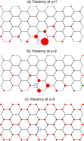
To understand the peculiar effects of single lattice vacancy on the metallic aGNR, we examine the microscopic distribution of LDOS of the ribbon. Figure 2(a) shows the LDOS distribution at when a single vacancy locates at , as marked by the square, where the magnitude of the LDOS is denoted by the radius of the solid circle. We can see that for the sublattice to which the vacancy belongs(say A sublattice), all the atoms have zero LDOS. Finite LDOS appear only on the other sublattice(B sublattice). It is this non-bonding state that gives rise to the zero conductance at , as shown in Fig. 1. When the energy deviates from zero, LDOS on A sublattice becomes finite, which opens possible hopping paths for electrons to cross the vacancy region, and thus provides finite conductance. Figure 2(b) shows the LDOS distribution when the vacancy locates at . We can see that the non-bonding state also appears. When the vacancy locates at , the situation is similar with that of , and . However, for a vacancy at , we see in Fig. 2(c) that the LDOS distribution is uniform at , and zero at . The pattern is the same throughout the energy region of the first conductance channel, which explains why the lowest conductance plateau is unaffected by the presence of a vacancy at shown in Fig. 1.
We first notice that the response of the system to a vacancy at can be explained by the wave function of a perfect aGNR HHLin ; Brey ; ZHX ,
| (2) |
with for electrons and holes, the phase difference between two sublattices. The wave function exhibits nodes at , which makes these sites insensitive to introduction of vacancy.
In order to understand the phenomenon that a single vacancy reduces the LDOS at all the atoms of the same sublattice to zero at , we go back to the Shrödinger equation for the tight-binding model. The wave functions at the three nearest neighbors of the atom should satisfy the relation
| (3) |
At zero energy, this implies
| (4) |
Without lost of generality, we take aGNR with width with a vacancy on the B sublattice, as shown by Fig. 3. Now we set a vacancy at the edge as marked by the square in Fig. 3, which renders . From the Shrödinger equation we can immediately get . Then from , due to the node of wave function of aGNR, and , we can deduce . In a similar way we can show that all the atoms of sublattice B have zero LDOS. It is easy to see that the same discussion applies for the vacancy at any positions of of the aGNR.
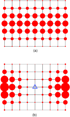
The appearance of such non-bonding state is closely related with the topological structure of graphene. A single vacancy cannot induce such non-bonding state for the square lattice, as shown by Fig. 4, where the triangle denotes the vacancy.
III Transport properties of armchair GNC
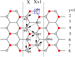
We now turn our attention to the armchair GNC shown in Fig. 5, with widths of the wide metallic aGNRs and the narrow one denoted by and , and the length of the central segment in units . Two vertical aligned zigzag boundaries are emphasized by the bold lines with the notation , . We first study the conductance as a function of .

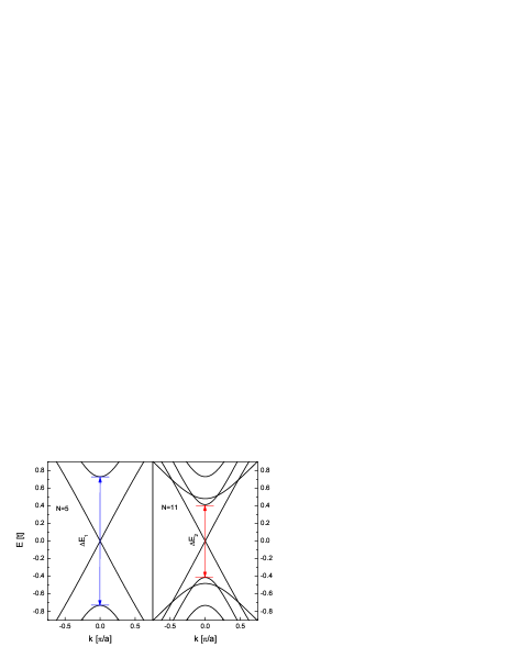

The band structures of aGNR with width 5 and 11 are shown in Fig. 6. In this paper, we will focus on the energy regime around the zero energy, in which both the wide and narrow aGNRs exhibit the single conduction channel. As in Fig. 7 we observe oscillating conductance with the peak value reaching , and a larger induces more rapid oscillations. Around , the conduction is suppressed to zero for all
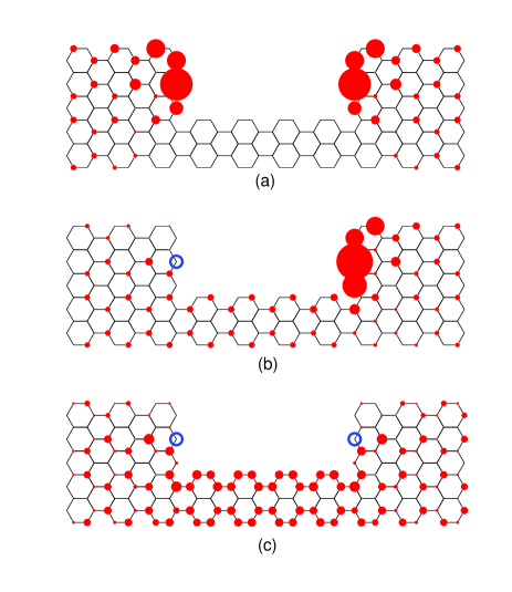

To understand the peculiar behaviors of the conductance of the GNC, we study the LDOS distribution. As in Fig. 8(a), there is a localized edge state at each ZB. We have also investigated ZB’s with different heights (4, 5, 6, 7, 8, 9 for GNC with wider aGNR ) and found that a ZB with three successive sites in a sequence is enough to induce localized edge state, consistent with previous works Nakada ; Yisong ; O.Hod . The localized edge state is suppressed by the introduction of a single vacancy at the ZB b1 and b2, as shown in Figs. 8(b) and (c).
Next we study how the localized edge states affect the transport behaviors by comparing the conductance spectrums of the three GNCs shown in Fig. 8. As shown in Figs. 9 (a) and (b), for the GNCs with one or two ZBs, the conductance is suppressed to zero near the zero Fermi energy. However, for a GNC without ZB, the conductance remains finite at , see Fig. 9 (c). Therefore, the localized state at the ZB is responsible for the suppression of conductance to zero at .
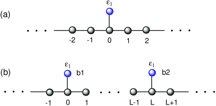
Since we are considering the energy region where both the wide aGNRs and the narrow one permit only one conducting channel, they can be modeled by a single nanowire. A ZB which induces localized state can be modeled by a quantum dot (QD) coupled to the nanowire. The model system is shown in Fig. 10. Here we would like to discuss the simpler case first, i.e., the model with a single QD. For this system, Orellana et al.Orellana have already solved the transmission coefficient by setting the wave function as
| (5) |
and matching the wave functions from both the left and right sides to that coupled by the QD. The conductance can be derived analytically as
| (6) |
where is the Fermi energy of the quantum wire, is the eigen energy of the side coupled by QD, is the hopping constant both within the nanowire and between the nanowire and QD. From Eq. (6) one can find that an antiresonance appears at the energy . The localized edge state at zero Fermi energyFujita implies , and explains why a single ZB of GNC induces a zero conductance at the zero Fermi energy. Figure. 9(a) shows the transmission spectrum of GNC with one ZB, which is well described by the simple model especially in the small region.
Similarly, the GNC with two ZBs, as shown in Fig. 8 (a), can be modeled by two QDs coupled to a nanowire, as shown by Fig. 10 (b). Now we extend the approach by Orellana et al.Orellana to the model with two QDs. The wave function should be
| (7) |
Solving the wave function matching equations, we obtain the transmission coefficients
| (8) |
where . Since diverges at , one has , and thus the transmission probability . Figure 9(b) shows the transmission spectrum of the model of two QDs. We find that the model can describe the GNC with two ZBs very well.
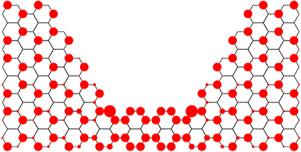
In the absence of ZB in the GNCs, there will be no localized state, and thus no antiresonance, which results in a normal oscillation of conductance without zero conductance valley, as shown by Fig. 9 (c). We also investigated GNCs with armchair boundaries, and found no localized edge states, as shown in Fig. 11, associated with finite conductance.
IV Summary
Using tight-binding approach and Green’s function method, we show that for a metallic aGNR with a single vacancy at , the zero conductance valley arises from a non-bonding state at the zero Fermi energy. Next, for the square-shaped armchair GNC consisting of three metallic aGNR segments, we find resonant tunneling behaviors in the energy regime with single conduction channel. It is shown that the localized edge state at the ZB affects the transport properties severely. A one dimensional model with one or two QDs coupled to a nanowire is put forward which can explain the resonant tunneling behavior of aGNC very well.
Acknowledgements.
The authors would like to thank P. A. Orellana and A. Tanaka for helpful discussions.References
- (1) K. S. Novoselov, A. K. Geim, S. V. Morozov, D. Jiang, Y. Zhang, S. V. Dubonos, I. V. Grigorieva, and A. A. Firsov, Science 306, 666 (2004).
- (2) P. R. Wallace, Physical Review 71, 622 (1947).
- (3) A. K. Geim and K. S. Novoselov, Nat Mater 6 , 183(2007).
- (4) M. S. Purewal, Y. Zhang and P. Kim, Phys. Stat. Sol.(b) 243, 3418 (2006).
- (5) A. H. Castro Neto, F. Guinea and N. M. R. Peres, K. S. Novosolev and A. K. Geim, Rev. Mod. Phys. 81, 109 (2009).
- (6) M. I.Katsnelson, Materials Today 10, 20(2007).
- (7) M. Fujita, K. Wakabayashi, K. Nakada and K. Kusakabe,J. Phys. Soc. Jpn. 65 1920,(1996)
- (8) K. Nakada, M. Fujita, G. Dresselhaus, and M. S. Dresselhaus, Phys. Rev. B. 54, 17954 (1996).
- (9) K. Wakabayashi, Physical Review B 64, 125428 (2001).
- (10) N. M. R. Peres, A. H. Castro Neto, and F. Guinea, Phys. Rev. B 73, 195411 (2006).
- (11) L. Brey and H. A. Fertig, Phys. Rev. B 73, 235411 (2006)
- (12) T. C. Li and S.-P. Lu, Phys. Rev.B 77, 085408 (2008).
- (13) B. Obradovic, R. Kotlyar, F. Heinz, P. Matagne, T. Rakshit, M. D. Giles, M. A. Stettlera, and D. E. Nikonov, Appl. Phys. Lett. 88, 142102 (2006)
- (14) Q. Yan, B. Huang, J. Yu, F. Zheng, J. Zang, J. Wu, B.-L. Gu, F. Liu, and W. Duan, Nano Lett. 7, 1469(2007)
- (15) G. Liang, N. Neophytou, M. S. Lundstrom and D. E. Nikonov, J. Appl. Phys. 102, 054307 (2007).
- (16) J. R. Williams, L. DiCarlo, C. M. Marcus, Science 317, 638 (2007)
- (17) D. A. Abanin and L. S. Levitov, Science 317, 641 (2007)
- (18) W. Long, Q. F. Sun, and J. Wang, Phys. Rev. Lett. 101, 166806 (2008).
- (19) J. Li, S. Q. Shen, Phys. Rev. B 78, 205308 (2008).
- (20) S. Hong, Y. Yoon, and J. Guo, Appl. Phys. Lett. 92, 083107 (2008).
- (21) H. Li, L. Wang and Y. Zheng, cond-mat/0808.0947
- (22) Y. P. Chen, Y. E. Xie, and X. H.Yan,, J. Appl. Phys. 103, 063711(2008).
- (23) Z. F. Wang, Q. W. Shi, Q. Li, X.Wang, J.G. Hou, H. Zheng, Y. Yao, J. Chen, Appl. Phys. Lett. 91, 053109 (2007).
- (24) Z. P. Xu and Q. S. Zheng, Appl. Phys. Lett. 90, 223115 (2007).
- (25) T. Jayasekera and J. W. Mintmire, Nanotechnology 18, 424033 (2007).
- (26) J.-Y. Yan, P. Zhang, B. Sun, H.-Z. Lu, Z. Wang, S. Duan, and X.-G. Zhao, Phys. Rev. B 79, 115403(2009).
- (27) Y. Zhang, J.-P. Hu, B. A. Bernevig, X. R. Wang, X. C. Xie, and W. M. Liu, Phys. Rev. B 78, 115413(2008).
- (28) D. A. Areshkin and C. T. White, Nano Lett. 7, 3253 (2007)
- (29) F. Muñoz-Rojas, D. Jacob, J. Fernández-Rossier, and J. J. Palacios, Phys. Rev. B. 74, 195417 (2006)
- (30) A. Rycerz, J. Tworzydło, and C. W. J. Beenakker, Nature Phys. 3, 172(2007).
- (31) B. Özyilmaz, P. Jarillo-Herrero, D. Efetov, and P. Kim, Appl. Phys. Lett. 91, 192107 (2007).
- (32) A. Chuvilin, J. C. Meyer, G. Algara-Siller, and U. Kaiser, New J. Phys. 11,083019 (2009).
- (33) P. Darancet, V. Olevano, and D. Mayou, Phys. Rev. Lett. 102, 136803(2009).
- (34) A. N. Andriotis, E. Richter, and M. Menon, Appl. Phys. Lett. 91, 152105 (2007).
- (35) K. Todd, H.-T. Chou, S. Amasha, and D. Goldhaber-Gordon, Nano Lett. 9, 416 (2009).
- (36) F. Molitor, A. Jacobsen, C. Stampfer, J. Güttinger, T. Ihn, and K. Ensslin, Phys. Rev. B 79, 075426(2009).
- (37) F. Muñoz-Rojas, J. Fernández-Rossier, L. Brey and J. J. Palacios, Phys. Rev. B. 77, 045301 (2008)
- (38) Chuanhong Jin, Haiping Lan, Lianmao Peng, Kazu Suenaga, and Sumio Iijima, Phys. Rev. Lett. 102, 205501 (2009)
- (39) O. Hod, V. Barone, and G. E. Scuseria, Phys. Rev. B 77, 035411 (2008).
- (40) M. P. L. Sancho, J. M. L. Sancho, J. Rubio, J. Phys. F: Met. Phys. 15, 851 (1985).
- (41) L. Chico, V. H. Crespi, L. X. Benedict, S. G. Louie, and M. L. Cohen, Phys. Rev. B, 54 2600(1996).
- (42) K. Wakabayashi, J. Phys. Soc. Jpn. 71, 2500 (2002).
- (43) H. H. Lin, T. Hikihara, H. T. Jeng, B. L. Huang, C .Y. Mou, and X. Hu, Phys. Rev. B. 79, 035405 (2009)
- (44) H. Zheng, Z. F. Wang, Tao Luo, Q. W. Shi, and J. Chen, Phys. Rev. B. 75, 165414 (2007)
- (45) P. A. Orellana, F. Domínguez-Adame, I. Gémez, and M. L. Ladrón de Guevara, Phys. Rev. B. 67, 085321 (2003)
- (46) M. P. L. Sancho, J. M. L. Sancho, and J. Rubio, J. Phys. F: Met. Phys. 14, 1205 (1984).
- (47) L. Chico, L. X. Benedict, S. G. Louie, and M. L. Cohen, Phys. Rev. B. 54, 2600 (1996)
- (48) S. Datta, Electronic Transport in Mesoscopic Systems (Cambridge University Press, Cambridge, 1995) .
- (49) K. Wakabayashi, and M. Sigrist, Phys. Rev. Lett. 84, 3390 (2000).