On the exploitability of thermo-charged capacitors
Abstract
Recently [Physics Letters A 374 (2010) 1801] the concept of vacuum
capacitor spontaneously charged harnessing the heat from a single
thermal reservoir at room temperature has been introduced, along with a
mathematical description of its functioning and a discussion on the main
paradoxical feature that seems to violate the Second Law of
Thermodynamics. In the present paper we investigate the theoretical and
practical possibility of exploiting such a thermo-charged capacitor as
voltage/current generator: we show that if very weak provisos on the
physical characteristics of the capacitor are fulfilled, then a non-zero
current should flow across the device, allowing the generation of
potentially usable voltage, current and electric power out of a single
thermal source at room temperature. Preliminary results show that the
power output is tiny but non-zero.
PACS (2010): 79.40.+z, 67.30.ef, 65.40.gd, 84.32.Tt
Keywords: thermionic emission capacitors
contact potential second law of thermodynamics
1 Introduction
In a recent paper [1], the author introduces the concept of vacuum capacitor spontaneously charged harnessing the heat absorbed from a single thermal reservoir at room temperature. It is called for brevity thermo-charged capacitor. Further, he presents a mathematical description of its basic functioning.
In the same paper, the author shows that, when the tools of the Classical Thermodynamics, e.g. the Clausius entropy variation analysis, are applied to the process, a paradox seems to arise: the macroscopic behavior of a thermo-charged capacitor appears to violate the Clausius formulation of the Second Law of Thermodynamics [1].
As a matter of fact, such a result should not be seen as so weird. Although no experimental violation has been claimed to date, over the past 10-15 years an unparalleled number of challenges has been proposed against the status of the Second Law of Thermodynamics. During this period, more than 50 papers have appeared in the refereed scientific literature (see, for example, references [5, 6, 7, 8, 9, 10, 11, 12, 13, 14, 15, 16, 17, 18, 19, 20, 21, 23, 24]), together with a monograph entirely devoted to this subject [3]. Moreover, during the same period two international conferences on the limit of the Second Law were also held [2, 4].
The general class of recent challenges [3, 20, 24] spans plasma [19], chemical [23], gravitational [12] and solid state physics [21, 22, 24]. Currently, all these approaches appear immune to standard Second Law defenses (for a compendium of the classical defenses, see [25]) and several of them account laboratory corroboration of their underlying physical processes.
In the present paper we investigate the theoretical and practical possibility of exploiting thermo-charged capacitors as voltage/current generators. In Section 2 we review the setup of the thermo-charged capacitor and its mathematical model, extending that presented in [1]. Here we drop an apparently crucial simplification made in [1] and show that the physical process presented in [1] is robust against such simplification.
In Section 3 we show that if very weak provisos on the physical characteristics of the capacitor are fulfilled, then a non-zero current should flow across the device, allowing the generation of potentially usable voltage, current and electric power out of a single thermal source at room temperature. Preliminary results show that the power output is tiny but non-zero.
If it were possible to experimentally and unambiguously achieve such results, then we would have an experimental violation of the Second Law in the Kelvin-Planck formulation, which parallels the alleged violation in its Clausius form discussed in [1]. In other words, we could have a sort of thermo-voltaic cell.
2 Thermo-charged spherical capacitor
In Fig. 1 a sketched section of the vacuum spherical capacitor is shown (see also [1]). The outer sphere has radius and it is made of metallic material with relatively high work function (eV). The inner sphere has radius and it is made of the same conductive material as the outer one, but it is coated with a layer of semiconductor Ag–O–Cs, which has a relatively low work function (eV). It should be clear that in such a case the two thermionic fluxes, from each plate toward the other one, are different, the latter being greater than the former, at least at the beginning of the charging process. The capacitor should be shielded by a case and put at room temperature. The case must be opaque to every environmental electromagnetic disturbance (natural and man-made e.m. waves, cosmic rays and so on) in order to avoid spurious photo-electric emission. Moreover, the outer plate should be externally insulated, in order to prevent its outward thermionic emission and the inter-plate space must be under extreme vacuum (UHV).
All the electrons emitted by the inner sphere, due to thermionic emission at room temperature, are collected by the outer (very low emitting) sphere, creating a macroscopic difference of potential . At first, such a process is unbalanced, being the flux from the inner sphere greater than that from the outer sphere, but later, with the increase of potential , the inward and the outward flux should tend to balance each other.
A crucial point for what follows is the behavior of the contact surface between the Ag–O–Cs layer and the conductive material of the inner sphere.
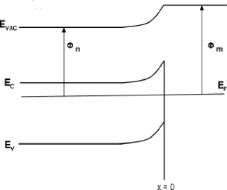
The contact surface between the inner metallic plate and the Ag–O–Cs layer is a well-known Schottky junction (metal/n–type semiconductor). When two materials (in our case, a metal and a semiconductor) are physically joined, so as to establish a uniform chemical potential, that is a single Fermi level, some electrons are transferred from the material with the lesser work function (Ag–O–Cs) to the material with the greater work function (metal). As a result, a contact potential is established such that . The junction is thus the region where, at equilibrium, a balance between bulk electrostatic and diffusive (thermally driven) forces is attained. The energy band profiles of semiconductor-metal junction at equilibrium are shown in Fig. 2. The feature which counts for the functioning of our device is the fact that the energy level of the vacuum for Ag–O–Cs (and that for the metallic plate) is preserved far from the depletion region [26].
This means that whenever an electron is extracted from the Ag–O–Cs layer to the vacuum (toward the outer sphere), and this is made always at the cost of eV for what is said above, Ag–O–Cs layer starts to charge up positively; hence, a sort of ‘external’ reverse bias starts to form across the junction and a tiny current of electrons begins to flow from the metallic inner sphere to the Ag–O–Cs layer in order to re-establish the equilibrium (constant contact potential).
Such a current flow is known as reverse bias leakage current (RLC). Its physical generating mechanisms are variegated and complex, and the amplitude is influenced by many factors like thickness of the depletion region, temperature, cross-sectional area and impurities of the junction, and so on. Also the amplitude of the reverse bias influences the intensity of RLC, although when the reverse bias is below the breakdown voltage of the junction (usually tens or hundreds of volts), the current changes slowly with bias.
It depends on the used material, but usually the reverse leakage current density , namely RLC per unit surface, spans111See, for example, [35, 36, 37, 38] for some specific types of Schottky and n–p junctions. Values greater than A/cm2 and lower than A/cm2 are also possible with the same reverse bias, depending on the materials, preparation, junction impurities and surface treatments. Usually, applied researchers and industry desire to lower the reverse leakage current in order to exalt the rectifying properties of the junction for electrical and electronic applications. Here, instead, we have opposite needs. from A/cm2 to A/cm2 for reverse biases of the order of volts or tenths of volts. As will be clear later, if we suitably increase the contact surface between the inner metallic sphere and the Ag–O–Cs layer, namely increase the surface of the inner sphere , then the RLC can be made of the order of A or greater, RLC being equal to . We can also be favored by junction impurities: they usually transform rectifying junctions into ohmic ones. All these issues will be treated more thoroughly in Section 3.
In almost all textbooks it is said that a voltage drop builds up not only across the contact surface (contact potential), but instantaneously also between the surfaces at the free ends of the materials as soon as they are joined at one end (see Fig. 3), where charges also accumulate (to the author’s knowledge, no textbook or published paper on the subject clearly explains where these charges come from). This voltage drop is of the same magnitude of the contact potential . All this is usually explained by appealing to a supposed straightforward application of the Kirchhoff’s second (loop) rule.
If this were true, then it should prevent any imbalance in electron emission between the inner and the outer sphere as soon as the two spheres are electrically shorted through an external resistor so as to form a circuit similar to that in Fig. 3. In that case, in order to reach the outer sphere, any electron escaping the inner layer would need the same energy needed by an electron escaping the outer sphere to reach the inner one. The inner electron needs an energy equal to , since it must be ejected (required energy ) and then it has to overcome the potential drop (energy equal to ). The outer electron needs (energy to be ejected). But, since =, the inner electron needs .
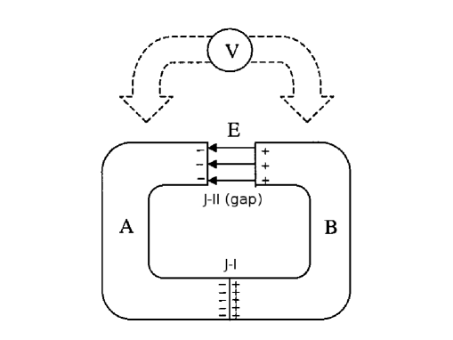
Such a situation would undoubtedly be one of equilibrium. But we have explicitly shown in [28] that no electric field, and thus no voltage drop, builds up between the surfaces at the free ends of two materials with different work functions as soon as the materials are physically joined at one end.
In [28] we presented three arguments: the first two were more heuristic, the third one was more theoretical. Let us sketch here the last one, namely an explicit application of the path-independence law and/or Kirchhoff’s loop rule. The physical principle at the basis of these two laws is the more fundamental law of conservation of energy. Conservation of energy demands that a test electronic charge conveyed around a closed path in the device bulk of Fig. 3, through J-I (physical junction) and J-II (gap) at equilibrium, must undergo zero net work from all the forces present along the path. Mathematically, we must have,
| (1) |
At equilibrium, the only two regions where forces are allowed to be non-zero are the J-I and J-II regions. An electric field elsewhere in A and B (other than in the contact region) would generate a current, which contradicts the assumption of equilibrium. When the test charge crosses J-I, it is subject to the built-in electric field force and to the diffusion force . This “force” is a thermally driven force and it is responsible for the establishment of the contact potential at J-I. We know that at equilibrium and that is different from zero and constantly present, otherwise would soon drop to zero, thus,
| (2) |
In the J-II gap there are no diffusion forces, since it is a vacuum gap, and eventually we have,
| (3) |
where is the gap width.
We now refine the estimate of the obtainable voltage and the estimate of the time needed to reach such a value, taking into account not only the physical characteristics of the capacitor and the quantum efficiency curve of thermionic material Ag–O–Cs (as made in [1]), but also the thermionic emission and the quantum efficiency curve of the outer sphere.
The capacitor is placed in a heat bath at room temperature and it is subject to the black-body radiation. Both spheres, at thermal equilibrium, emit and absorb an equal amount of radiation (Kirchhoff’s law of thermal radiation), thus the amount of radiation absorbed by the spheres is the same as that emitted by those spheres according to the black-body radiation formula (Planck equation). Hence, given the room temperature , the Planck equation provides us with the number distribution of photons absorbed as a function of their frequency.
According to the law of thermionic emission, the kinetic energy of an electron emitted by the material is given by the following equation,
| (4) |
where is the energy of the photon with frequency ( is the Planck constant) and is the work function of the material. Thus, only the tail of the Planck distribution of the absorbed photons, with frequency , can contribute to thermionic emission.
An electron emitted by the inner sphere, thanks to the absorption of a photon of frequency , is able to reach the outer sphere with zero velocity only when,
| (5) |
where is the inter-sphere voltage reached so far. On the other hand, an electron of the outer sphere does not have to overcome an opposed voltage in order to reach the inner sphere, and thus the following holds,
| (6) |
Hence, we have the following useful relations,
| (7) |
| (8) |
which give the minimum frequencies of radiation with enough energy to move an electron from one sphere to the other.
The total number of photons per unit time with energy greater than or equal to , emitted and absorbed in thermal equilibrium by the inner sphere is given by the Planck equation,
| (9) |
where is the inner sphere surface area, is the speed of light, is the Boltzmann constant and the room temperature.
If is the quantum efficiency (or quantum yield) curve of the Ag–O–Cs thermionic layer, then the number of electrons per unit time emitted by the inner sphere towards the outer sphere with kinetic energy greater than or equal to , is given by,
| (10) |
where is the surface area of the inner sphere.
Following the same reasoning, the number of electrons per unit time emitted by the outer sphere and collected by the inner one is given by the analogous relation,
| (11) |
In this last relation it is not easy to define the multiplicative factor related to the surface area: before the charging process starts, is equal to the inner sphere surface area , but as soon as the inner sphere charges up positively, its effective surface area increases due to the electrostatic focusing effect (similar to the gravitational focusing effect). Moreover, it is not easy to mathematically model such a phenomenon since the effective area of the inner sphere depends on the velocity of the single electron flying toward it. Here we decide to be extremely conservative and choose equal to the surface area of the outer sphere. As a matter of fact, the following results are practically independent of the choice of any reasonable value of .
For a vacuum spherical capacitor, the voltage between the spheres and the charge on each sphere are linked by the following well-known equation,
| (12) |
Now, we derive the differential equation which governs the process of thermo-charging. In the interval of time the charge collected by the outer sphere is given by,
| (13) |
where we make use of eqs. (7) and (8) for and , and is the voltage at time . Thus, through the differential form of eq. (12), we have,
| (14) |
or
| (15) |
Since our aim is to maximize the value of , we have to choose and such that they maximize the geometrical factor . The rightmost integral of eq. (15) has a smaller value with respect to the leftmost one by some orders of magnitude, at least at the beginning of the charging process, hence what counts for the maximization of is the maximization of the factor alone.
It is not difficult to see that the maximum is reached when . So we have,
| (16) |
In the rest of this Section we provide a numerical solution of the above differential equation for the practical case of inner sphere coated with a layer of Ag–O–Cs [29, 30, 32]. To do that we need to adopt an approximation, however: the approximation consists in the adoption of a constant value for the functions , a sort of suitable mean values .
The differential equation (16) thus becomes,
| (17) |
A straightforward variable substitution in the integrals of eq. (17) allows to write the equation in its final simplified form,
| (18) |
Here we provide an exemplificative numerical solution of eq. (18), adopting the following nominal values for , , , and and : eV, eV, m, K, , and .
In order to make a conservative choice for the value of we note that only black-body radiation with frequency greater than can contribute to thermionic emission. This means that, for the Ag–O–Cs photo-cathode, only radiation with wavelength smaller than nm contributes to the emission. According to Fig. 1 in [32, Bates], the quantum yield of Ag–O–Cs for wavelengths smaller than (and thus, for frequency greater than ) is always greater than .
For what concerns , its value is related (as it is for the value of ) to the discharging process due to counter emission. As a matter of fact, thermionic counter emission can be kept extremely low with value of high compared to , and also choosing suitable metallic material for the outer sphere, with very low , namely .
There are also other possible sources of counter emission, e. g. secondary electron emission [31], but as far as we known they are always smaller than the charging emission (and they can be made very weak with particular design, choice of material and surface texture of the outer sphere). In any case, counter emissions should only retard the achievement of the equilibrium voltage , not preclude it. Any such delay in time can be easily modeled with the same eq. (18), simply changing the numerical value of , , and .
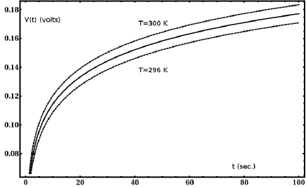
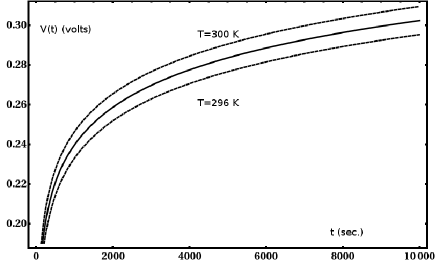
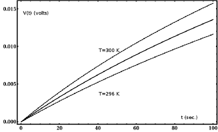
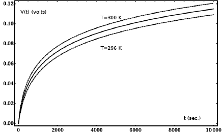
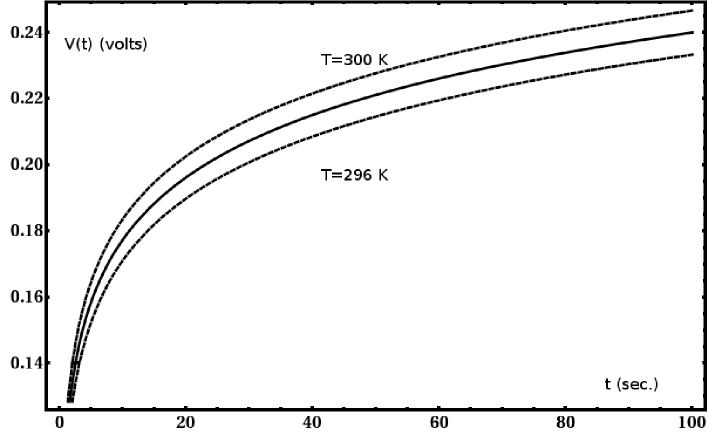
In order to have the least involved sample solution of eq. (18), we adopted the very conservative choice of . In Fig. 4 the numerical solution of the above test is shown. In plot (a) we could easily see how only after 60 seconds the voltage of the capacitor may exceed the value of volts. Plot (b) tells us that the voltage of the capacitor requires some hours to approach volts. Even in the more pessimistic scenario where , we see that a macroscopic voltage should arise quite rapidly between the plates; see Fig. 5.
For the sake of completeness, in Fig. 4 and Fig. 5 charging profiles for K and for K are also shown in order to give an hint on how eq. (18) behaves with temperature. From the experimental point of view this information is important since it is hard to maintain the temperature of the environment precisely at K.
As can be easily noted, the charging profiles at K in Fig. 4 and Fig. 5 are exactly the same of those in Fig. 2 and Fig. 3 of [1]. All this has a twofold meaning. First of all, even with five orders of magnitude greater than , the counter emission disturbance on the charging process is negligible and, as said before, it would become more negligible with the suggested choice of , as is clear from the mathematics of eq. (18).
More important, the physical process firstly introduced in [1] and under study in the present paper is quite robust against the dropping of the approximation made in [1], namely or . Moreover, from the experimental point of view, the physical process appears to be not so sensible to the specific value of , provided that eV.
3 Discussion
In this Section we show quantitatively how it is possible to make a measurable current flow across the thermo-charged capacitor, once its plates are electrically shunted by a suitable resistor, and hence allowing the generation of potentially usable voltage, current and electric power out of a single thermal source at room temperature (like an ordinary battery). In the following, we also try to answer some objections, which should naturally and suddenly arise against our results.
As explained in Section 2, thermionic emission produces a bias between the plates of the spherical capacitor (Figs. 4 and 5). A similar bias also arises across the junction metal/semiconductor (since the Ag–O–Cs layer charges up positively) of the inner sphere: given the nature of the metal/Ag–O–Cs junction, such a bias has the characteristics of a reverse bias. The reverse bias causes a reverse leakage density current , as explained in Section 2, which slowly transfers electrons from the inner metallic sphere to the Ag–O–Cs layer. This reverse leakage density current is microscopic, usually ranging from A/cm2 to A/cm2 for reverse biases of the order of volts or tenths of volts, and its intensity is weakly dependent on the magnitude of the reverse bias, provided that such a bias is below the breakdown voltage of the junction [35, 36, 37, 38]. As seen in the previous Section, our device is far below that voltage.
Now, the mere fact that a non-zero, almost constant, reverse bias leakage density current exists, although very tiny, let the thermo-charging process be potentially exploitable. As a matter of fact, if we suitably increase the surface area of the inner sphere (and also that of the outer one, accordingly), then the contact area between the Ag–O–Cs layer and the metal increases. This means that in principle it is possible to obtain a macroscopic reverse leakage current (RLC) that allows a rather quick transfer of the voltage drop to both the terminal leads of the capacitor, since RLC is equal to .
For the sake of thought experiment, imagine to build a room-sized thermo-charged capacitor with radii cm and cm. In this case the inner sphere surface is equal to cm2. Thus, the total reverse leakage current should vary between mA and mA; this is a quite macroscopic current. The thermo-charging profile for the capacitor with the following parameters eV, eV, m, K, and , is represented in Fig. 6.
Let us now compare the RLC in this case with the thermionic current between the spheres at s (and V). It should be clear that the value of at s is the maximum value reachable by the thermionic current during the charging process. Rearranging eq. (13) and eq. (18) we obtain,
| (19) |
and through numerical calculations for s we get A.
We note that and this means that the voltage drop thermally gained within the plates of the capacitor is quickly transferred to both terminal (metallic) leads of the capacitor and can be directly detected through an electroscope.
But we can do better. It is possible to directly compare the reverse bias leakage density current with the thermionic density current, , obtained from eq. (19) as follows
| (20) |
assuming the maximizing condition for (see eq. (16)).
Thus, for eV, eV, K, , and in the reasonable range given before, we see from eq. (20) that is always greater that : this roughly means that the voltage drop thermally gained within the plates of the capacitor is always quickly transferred to both terminal (metallic) leads of the capacitor, no matter how big or small is the capacitor. Obviously, the bigger is the capacitor, the greater will be the current ‘flowing’ through it.
Let us now consider the capacitor of Fig. 1 shunted by a suitable resistor . In this case the capacitor behaves like a battery which dissipates its power through the resistor (Joule effect).
Consider the electrical circuit depicted in Fig. 7. In steady state conditions, voltage drop and current should be the same across the capacitor and the resistor; moreover, they should be constant in time. According to Ohm’s Law, we must have , and this relation also gives the numerical value of the resistance needed to have these particular values of and .
Given the equations of the thermo-charged capacitor described before, we must have,
| (21) |
The power provided by the thermo-charged capacitor is calculated as,
| (22) |
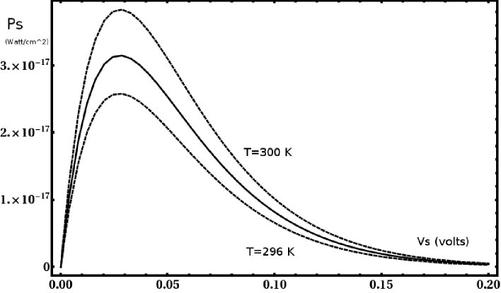
The power per unit surface of the inner sphere is then,
| (23) |
In Fig. 8 the power is plotted against the steady state voltage . For the capacitors described in this paper, namely that with cm, cm2 and that with cm, cm2, we obtain Watts and Watts, respectively. These are quite microscopic power outputs indeed, considering further that the second capacitor described has ‘uncomfortable’ room-sized dimensions.
There are now few doubts that one of the definite results of our paper is that the thermo-charged capacitors described here are highly ‘ineffective’. Anyway, it is important to experimentally test their functioning, since if they work according to the analysis done in this paper, then we would have a reproducible Second Law violation: therefore, we believe that its smallness is a secondary problem (that can be overcome with further future research), provided that this smallness is not to forbid a clear and unambiguous result with confounding environmental factors.
We have seen that the current and the power outputs of circuits like those depicted in Fig. 7 are microscopic, in particular if the physical dimensions of the spheres are centimetric. Nevertheless, the voltage drop of non-shunted capacitors is macroscopic (of the order of V), already for a single capacitor: thus, it should not be difficult to build tens of centimetre-sized vacuum capacitors, wired in series, so as to produce a voltage drop of volts or tens of volts. This output is far from the risk to be ambiguously interpreted.
From an experimental perspective, some manufacturing difficulties have to be faced. For example, stable ultra-high vacuum required inside the capacitor may pose a technical challenge, mainly for metre-sized device. Nonetheless, vacuum technology is currently quite sophisticated and mature and we expect that the construction of light, vacuum-proof centimetre-sized capacitors should not pose any concern at all.
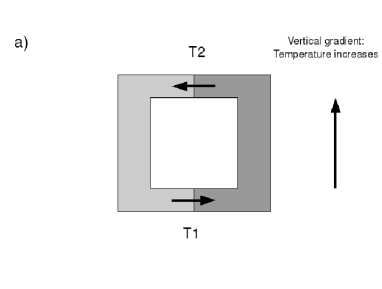
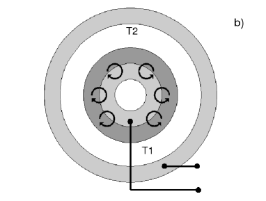
One issue that may be experimentally important is how the naturally present spatial thermal gradient222Like that usually present inside a room between floor and ceiling. affects the functioning of our capacitor. The inner sphere being made of two materials with different work functions in contact, one may expect the presence of the well-known thermocouple (voltage/current) effect (see Fig. 9-a), that could make difficult and ambiguous the verification of the phenomenon described in this paper.
As a matter of fact, the geometry of our capacitor is such that a macroscopic thermal gradient across the inner sphere should not significantly affect the verification of our results: as shown in Fig. 9-b any possible thermocouple current remains confined inside the inner sphere, and the thermocouple voltage is zero being the thermocouple ‘shunted’. This confounding factor could be greatly reduced if it were possible to perform the experiment in micro-gravity environment, like, for example, that on International Space Station (ISS). Moreover, the use of many small (centimetre-sized) capacitors, rather than a single metre-sized one, greatly reduces the problem.
For what concerns another possible disturbing effect, the Thomson effect333Voltage/current generation due to temperature gradient within a system made of a single material., one can imagine to build an identical copy of our capacitor without the Ag–O–Cs coating on the inner sphere and to place it in the same environment of our main capacitor, side by side. In such a way, one can use the (possible) output of the “uncoated” capacitor, due to the Thomson effect, to cancel out the disturbance in our main capacitor due to the same effect.
Finally, let us now anticipate (and try to exhaustively respond to) some possible critics. Among the main objections to our results, probably the first one is that our device appears to suffer the same shortcomings of the self-rectifying diode scheme (see, for example, [33, Brillouin] and [34, McFee] and the references therein). We have to stress that our device is quite different from a solid-state diode: in solid-state diodes the physical contact, through the n–p junction, between the two terminals and the dynamic balance between the built-in electric field and diffusion forces across the junction prevent the establishment of a non-random, steady charge movement far from the depletion region toward the terminals, and thus the creation of a voltage drop between the terminal leads.
In our device, the presence of vacuum between the outer sphere and the inner one (there is no physical contact inside the capacitor), and the fact that only one sphere is covered with a low work function material, do not allow the above dynamic balance, and a definite, one-way migration of charges across the plates (to the terminal leads) should be possible, as described above.
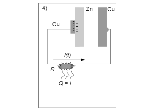
4 Electro-mechanical analogue of a thermo-charged capacitor
Thermo-charged capacitor has an easily understandable electro-mechanical analogue, which is both instructive and explicative and thus worthwhile to describe.
Consider the device depicted in Fig. 10-1. It is essentially a parallel plates capacitor with one plate made of a metal with relatively low work function, e.g. zinc (Zn), and the other one made of a relatively high work function metal, e.g. copper (Cu). This last plate is also free to move in the space. Moreover, a copper wire (with a load ) is connected to the zinc plate through a small junction Cu-Zn. The Cu-Zn junction generates a very thin (the junction being a metal to metal one) depletion layer along the contact surface, where positive and negative charges are localized after the dynamically balanced drift of electrons from zinc to copper through the contact area (Fig. 10-1).
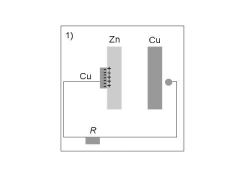
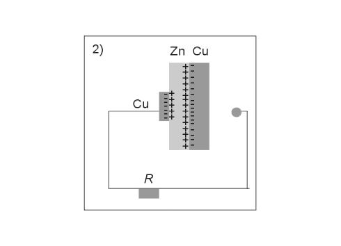
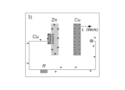
The first step of the electro-mechanical cycle we are going to describe consists in moving the copper plate toward the zinc one until the contact. In this phase no significant external work is required. After the contact, a second (and greater) depletion layer forms between zinc and copper plates. Also in this case, the new Cu-Zn junction generates a very thin depletion layer along the new (and wider) contact surface (Fig. 10-2).
In step two, an external work is applied to the copper plate in order to remove it from the zinc plate: is different from zero since the previous charges displacement across the new Cu-Zn junction makes the two plates attract each other. When the two plates are again suitably removed, the charges, initially localized within the thin depletion layer, are free to spread across the surfaces of the two metallic plates and wire, satisfying equi-potentiality (Fig. 10-3; see, for example, [39]).
In the third step of our cycle, we put the negatively charged copper plate and the positively charged copper wire into contact (Fig. 10-4). As soon as the contact is made, electrons start to flow from copper plate to zinc plate across the copper wire/load until both plates become neutral. Due to the Joule effect in the discharge, the load heats up. The amount of heat transferred to the environment is nearly equal to the external work done to the system in step number two (First Law of Thermodynamics).
The fourth step, that closes the cycle, is trivial and consists in moving the copper plate to its initial position, as in Fig. 10-1.
The analogy between this scheme and the thermo-charged capacitor should be clear: both devices work with materials having different work functions, and in both devices current (electrons) flows across contact junctions to re-establish electrical equilibrium.
The main difference is in the source of the energy needed to make the current flow. In the electro-mechanical scheme the source is the external work done to the system through the movable copper plate. In the thermo-charged capacitor it is the black-body radiation (of the uniformly heated environment) which provides the kinetic energy to electrons and let them fly to the external (fixed) plate of the capacitor.
Acknowledgements
This work has been partially supported by the Italian Space Agency under ASI Contract No. 1/015/07/0. The author thanks the three anonymous reviewers for their comments and suggestions.
References
- [1] G. D’Abramo, Phys. Lett. A 374 (2010) 1801.
- [2] D. P. Sheehan (Ed.), First International Conference on Quantum Limits to the Second Law, AIP Conference Proceedings, Vol. 643, AIP Press, Melville, NY, 2002.
- [3] V. Čápek, D. P. Sheehan, Challenges to the Second Law of Thermodynamics–Theory and Experiments, Fundamental Theories of Physics, Vol. 146, Springer, Dordrecht, Netherlands, 2005.
- [4] D. P. Sheehan (Ed.), The Second Law of Thermodynamics: Foundation and Status, Proceedings of Symposium at 87th Annual Meeting of the Pacific Division of AAAS, University of San Diego, June 19–22, 2006; Special Issue of Found. Phys. 37 (2007).
-
[5]
L.G.M. Gordon, Found. Phys. 11 (1981) 103;
L.G.M. Gordon, Found. Phys. 13 (1983) 989;
L.G.M. Gordon, J. Coll. Interf. Sci. 162 (1994) 512;
L.G.M. Gordon, Entropy 6 (2004) 38, 87, 86. -
[6]
J. Denur, Am. J. Phys. 49 (1981) 352;
J. Denur, Phys. Rev. A 40 (1989) 5390;
J. Denur, Entropy 6 (2004) 76. -
[7]
V. Čápek, J. Phys. A 30 (1997) 5245;
V. Čápek, Czech. J. Phys. 48 (1998) 993;
V. Čápek, Czech. J. Phys. 47 (1997) 845;
V. Čápek, Czech. J. Phys. 48 (1998) 879;
V. Čápek, Mol. Cryst. Liq. Cryst. 335 (2001) 24;
V. Čápek, J. Bok, J. Phys. A 31 (1998) 8745;
V. Čápek, Physica A 290 (2001) 379;
V. Čápek, T. Mančal, Europhys. Lett. 48 (1999) 365;
V. Čápek, T. Mančal, J. Phys. A 35 (2002) 2111;
V. Čápek, D. P. Sheehan, Physica A 304 (2002) 461. - [8] J. Bok, V. Čápek, Entropy 6 (2004) 57.
-
[9]
A. E. Allahverdyan, Th. M. Nieuwenhuizen, Phys. Rev. Lett.
85 (2000) 1799;
A. E. Allahverdyan, Th. M. Nieuwenhuizen, Phys. Rev. E 64 (2001) 056117;
A. E. Allahverdyan, Th. M. Nieuwenhuizen, Phys. Rev. B 66 (2003) 115309;
A. E. Allahverdyan, Th. M. Nieuwenhuizen, J. Phys. A 36 (2004) 875. - [10] Th. M. Nieuwenhuizen, A. E. Allahverdyan, Phys. Rev. E 66 (2002) 036102.
-
[11]
B. Crosignani, P. Di Porto, Am. J. Phys. 64 (1996) 610;
B. Crosignani, P. Di Porto, Europhys. Lett. 53 (2001) 290;
B. Crosignani, P. Di Porto, C. Conti, in: Quantum Limits to the Second Law, p. 267
B. Crosignani, P. Di Porto, C. Conti, Entropy 6 (2004) 50. -
[12]
D. P. Sheehan, J. Glick, J. D. Means, Found. Phys. 30 (2000)
1227;
D. P. Sheehan, J. Glick, Phys. Scr. 61 (2000) 635;
D. P. Sheehan, J. Glick, T. Duncan, J. A. Langton, M. J. Gagliardi, R. Tobe, Found. Phys. 32 (2002) 441;
D. P. Sheehan, J. Glick, T. Duncan, J. A. Langton, M. J. Gagliardi, R. Tobe, Phys. Scr. 65 (2002) 430. - [13] A. Trupp, in: Quantum Limits to the Second Law, p. 201, 231.
-
[14]
P. Keefe, J. Appl. Opt. 50 (2003) 2443;
P. Keefe, Entropy 6 (2004) 116. -
[15]
J. Berger, Phys. Rev. B 70 (2004) 024524.
J. Berger, Physica E 29 (2005) 100.
J. Berger, Found. Phys. 37 (2007) 1738. - [16] S. V. Dubonos, V. I. Kuznetsov, I. N. Zhilyaev, A. V. Nikulov, A. A. Firsov, JETP Lett. 77 (2003) 371.
-
[17]
A. V. Nikulov, Phys. Rev. B 64 (2001) 012505;
A. V. Nikulov, I. N. Zhilyaev, J. Low Temp. Phys. 112 (1998) 227. - [18] C. Pombo, A. E. Allahverdyan, Th. M. Nieuwenhuizen, in: Quantum Limits to the Second Law, p. 254.
-
[19]
D. P. Sheehan, Phys. Plasmas 2 (1995) 1893;
D. P. Sheehan, Phys. Plasmas 3 (1996) 104;
D. P. Sheehan, J. D. Means, Phys. Plasmas 5 (1998) 2469. - [20] D. P. Sheehan, J. Sci. Expl. 12 (1998) 303.
-
[21]
D. P. Sheehan, J. H. Wright, A. R. Putnam, Found. Phys. 32
(2002) 1557;
D. P. Sheehan, J. H. Wright, A. R. Putnam, A. K. Pertuu, Physica E 29 (2005) 87. - [22] D. P. Sheehan, D. H. E. Gross, Physica A 370 (2006) 461.
-
[23]
D. P. Sheehan, Phys. Rev. E 57 (1998) 6660.
D. P. Sheehan, Physica A 280 (2001) 185. - [24] D. P. Sheehan, J. Sci. Expl. 22 (2008) 459.
- [25] J. Earman, J. Norton, Stud. Hist. Phil. Mod. Phys. 29 (1998) 435.
- [26] Uebbing, J.J., James, L.W., J. Appl. Phys. 41(11) (1970) 4505.
- [27] Klein, U., Vollmann, W., Abatti, P.J., IEEE Transactions on Education, 46 (2003) 338.
- [28] D’Abramo, G., Found. Phys. 42 (2012) 369.
- [29] Sommer, A.H.: Photoemissive materials: preparation, properties, and uses. Section 7.1, Chapter 10. John Wiley & Sons (1936).
- [30] Sommer, A.H.: Multi-Alkali Photo Cathode. IRE Transactions on Nuclear Science, pp. 8–12. Invited paper presented at Scintillation Counter Symposium, Washington, D.C., February 28-29 1956.
- [31] Gimpel, I., Richardson, O., Proc. R. Soc. Lond. A 182 (1943) 17.
- [32] Bates Jr., C.W., Phys. Rev. Lett. 47(3) (1981) 204.
- [33] Brillouin, J., Phys. Rev. 78(5) (1950) 627.
- [34] McFee, R., Am. J. Phys. 59 (1971) 814.
- [35] Oyama, S., Hashizume, T., Hasegawa, H. Appl. Surf. Sci. 190 (2002) 322.
- [36] Rossi, D. V., Fossum, E. R., Pettit, G. D., Kirchner, P. D., Woodall, J. M., J. Vac. Sci. Technol. B 5(4) (1987) 982.
- [37] Hsu, J. W. P., Manfra, M. J., Lang, D. V., Richter, S., Chu, S. N. G., Sergent, A. M., Kleiman, R. N., Pfeiffer, L. N., Molnar, R. J., Appl. Phys. Lett. 78(12) (2001) 1685.
- [38] Dannhäuser, F., Solid State Electronics 10 (1967) 361.
- [39] Cotti, P., Physica B 204 (1995) 367.