Probing multiband superconductivity by point-contact spectroscopy
Abstract
Point-contact spectroscopy was originally developed for the determination of the electron-phonon spectral function in normal metals. However, in the past 20 years it has become an important tool in the investigation of superconductors. As a matter of fact, point contacts between a normal metal and a superconductor can provide information on the amplitude and symmetry of the energy gap that, in the superconducting state, opens up at the Fermi level. In this paper we review the experimental and theoretical aspects of point-contact spectroscopy in superconductors, and we give an experimental survey of the most recent applications of this technique to anisotropic and multiband superconductors.
I Introduction: point-contact spectroscopy
Point-contact spectroscopy (PCS) was developed more than 35 years ago as an experimental tool to investigate the interaction mechanisms between electrons and phonons in metals. Yanson yanson74 was the first to observe that small microconstrictions between two metals show non-linearities in the - characteristic (and in the second derivative ) that are the hallmark of inelastic scattering of electrons by phonons. The point-contact technique was later used to study all kinds of scattering of electrons by elementary excitation in metals, like magnons and so on duif89 ; naidyuklibro . When one of the sides of a point contact is a superconductor, quantum phenomena such as quasiparticle tunneling or Andreev reflection (see Sect.IV.1) occur at the interface, depending on the height of the potential barrier between the two electrodes. As a result, the shows – in addition to the features related to inelastic electron scattering – much stronger non-linearities that give rise to particular structures in the first derivative (that is, in the differential conductance) which contain fundamental information on the excitation spectrum of the quasiparticles, i.e. on the superconducting energy gap and its properties in the direct and reciprocal space. For this reason, and apparently in spite of its simplicity, point-contact spectroscopy has become an important, sometimes unique, tool for the investigation of superconducting materials. In some recent cases, PCS has provided precious spectroscopic information on newly discovered superconductors when more complex, technologically demanding techniques such as scanning tunneling microscopy (STM) and angle-resolved photoemission spectroscopy (ARPES) were still hindered by the absence of single-crystal samples of sufficient size. There is a number of excellent reviews that deal with the theoretical and experimental aspects of point-contact spectroscopy in normal metals and superconductors jansen80 ; duif89 ; naidyuklibro . An extensive and comprehensive review was dedicated especially to point-contact results in cuprates deutscher05 . The present review is therefore focused on the most recent applications of point contact spectroscopy to the study of multiband superconductors. A general theoretical introduction is provided, whose aim is to explain in a simple, experimental-oriented way, and with a consistent notation, theoretical models of increasing complexity for the interpretation of point-contact data in superconductors.
II Fabrication of point contacts
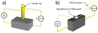
A point contact is simply a contact between two metals, or a metal and a superconductor, whose radius is smaller than the electron mean free path, and this in most cases means that the contact is nanometric. Historically, point contacts were fabricated in a number of ways naidyuklibro . The pioneering technique exploited by Yanson yanson74 for PCS was based on the realization of microshorts in the dielectric layer of a tunnel junction between two metals. Another technique widely used especially in superconductors (but that allows only the creation of homocontacts between two electrodes of the same material) is the break-junction technique in which a single sample is broken at low temperature into two pieces that are then brought back in contact. More recently, point contacts have been made by lithographical creation of a small hole in a thin membrane on both sides of which a metal film is then deposited. But the most used technique simply consists in bringing the two electrodes in contact by using a micromechanical apparatus. In the most common configuration, often called “needle-anvil”, the sample to be studied is one of the electrodes, and the other is a metallic tip, electrochemically or mechanically sharpened, which is gently pressed against the sample surface (figure 1a). Typically, the tip has an ending diameter of some tens of micrometers and it is easily deformed during the contact blonder83 . This means that, except in very special cases srikanth92 , parallel contacts are very likely to form between sample and tip baltz09 . In general this is not detrimental to spectroscopy, unless the sample is highly inhomogeneous on a length scale comparable with the tip end baltz09 . The needle-anvil technique has several advantages: i) it is non-destructive and several measurements can be carried out in the same samples; ii) the resistance of the contact can be controlled to some extent by fine tuning of the pressure applied by the tip. Its main drawbacks are the poor thermal and mechanical stability of the junction and the fact that, if the sample is very small (tens of micrometers, as it can happen with single crystals), the whole procedure becomes extremely difficult. For these reasons, since 2001 we adopted the so-called “soft” point-contact technique, in which the contact is made between the clean sample surface and a small drop (about 50 m in diameter) of Ag paste or a small In flake. The Ag or In counterelectrode is connected to current and voltage leads through a thin Au wire (10 - 25 m in diameter) stretched over the sample, as depicted in Fig 1(b). Despite the large “footprint” of the counterelectrode (in particular in the case of Ag paste) if compared to the electronic mean free path, these contacts very often provide spectroscopic information. This clearly means that, on a microscopic scale, the real electrical contact occurs only here and there through parallel nanometric channels connecting the sample surface with the In flake or with individual grains in the Ag paste, whose size is 2-10 m. With respect to the needle-anvil technique, the “soft” one does not involve any pressure applied to the sample and this can be sometimes very useful, as we will show in Sect. VII.3. The resistance of the as-made contacts is usually already in the suitable range for Andreev reflection to occur. If needed, it can be tuned by applying short ( ) voltage or current pulses until a spectroscopic contact is achieved. This effect (sometimes called “fritting” holm58 ) is well known in standard electrotechnics. The pulses have the effect of destroying some of the existing microjunctions and/or creating new ones by piercing a small oxide layer on the surface of either electrode. The contacts are mechanically and thermally very stable so that, for example, PCS measurements can be performed even in a cryocooler. Moreover, they can be made also on the thin side of small single crystals allowing directional point-contact spectroscopy even in samples too small for the needle-anvil technique. Often (but not always) the conductance curves of “soft” point contacts are more broadened than those obtained by the needle-anvil technique. As we will show, this is probably related to inelastic scattering near the interface, possibly by an oxide layer on the surface of Ag grains or of the sample. As a matter of fact, the same holds for contacts made with the Au wire alone, or even with a tip, whenever the pressure applied by the tip on the sample is small.
III Point-contact spectroscopy (PCS) in the normal state
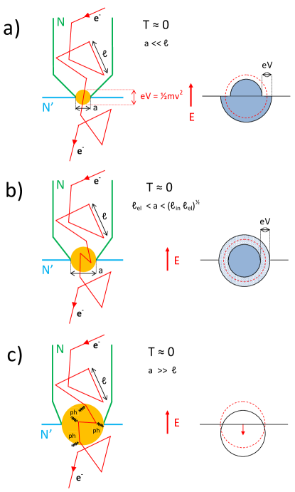
The uniqueness of point-contact spectroscopy in the normal state is due to its ability to provide spectroscopic, energy-resolved information on the inelastic scattering of quasiparticles with elementary excitations like phonons, magnons and so on by using a very simple and cheap experimental setup. To do so, however, some important experimental requirements must be fulfilled. The relevant quantity is the Knudsen ratio , where is the electron mean free path ( where are the elastic and inelastic mean free paths) and a is the contact radius. From now on it will be assumed that the shape of the contact is a circular orifice with radius a in an otherwise completely reflecting barrier. Unless otherwise specified, we will specially refer to homocontacts (i.e. contacts between two electrodes made of the same metal). Depending on the value of the Knudsen ratio, different regimes of conduction are possible, as described in the following.
III.0.1 Ballistic regime
In the ballistic regime the electron mean free path is much larger than the contact radius a ( or ). The applied voltage accelerates electrons within the distance of a mean free path. The electrons will then flow through the contact ballistically (with no scattering) gaining a kinetic energy equal to (see Fig. 2 (a)). In this way, the energy of the injected electrons is perfectly known and corresponds to the voltage applied to the junction. The resistance of the contact in such a situation was calculated by Sharvin sharvin65 and is equal to
| (1) |
where is the resistivity of the material under study. Since in metals , is independent of the electron mean free path, and depends only on the contact geometry. As a matter of fact, it can also be written as
| (2) |
being the Fermi momentum deJong94 . In the space, the (supposed spherical) Fermi surface (FS) expands for forward electrons by a quantity (see Fig.2(a)). Inelastic scattering events taking place in the bottom electrode give rise to a measurable (negative) corrections to the current only if they cause the backflow of carriers through the orifice. The backscattered electron must jump back onto the shrunk FS and this is possible only if it can lose an energy in the scattering process. This explains why in the ballistic regime the applied voltage sets the energy scale of the spectroscopic investigation.
The first-order correction to the current due to the backscattered electrons is duif89 ; naidyuklibro :
| (3) |
where is the effective volume in which the inelastic scattering of electrons contributing to occurs, is the density of states at the Fermi level and
| (4) |
is the spectral function for the relevant interaction, which results from an integration over all the initial and final electron states of the scattering matrix elements weighted by an efficiency function which accounts for the direction of the incoming and the inelastically scattered electron. It can be shown duif89 ; naidyuklibro that
| (5) |
A direct determination of the spectral function by means of PCS measurements is thus possible. If the elementary excitations are phonons, is the so called “point-contact electron-phonon spectral function” which differs only slightly (due to the efficiency function ) from the thermodynamic Eliashberg function . In this case, using the formulas of the free electron model, one obtains:
| (6) |
It is worth mentioning that, according to eq.6, one expects the experimental to rapidly fall to zero above the Debye energy. Very often this is not the case jansen80 ; duif89 ; naidyuklibro and a considerable background is found, which has been attributed to the presence of non-equilibrium phonons. It is however possible to correct for the background and to determine the function duif89 . This method has allowed extracting the electron-phonon spectral function in many normal metals naidyuklibro , but can be applied also to superconductors above the critical temperature or driven normal by means of a magnetic field. Some examples will be discussed in Sect. VII.2.3 for the case of MgB2 and in Sect. VII.4 for the case of borocarbides.
III.0.2 Thermal regime
As opposed to the ballistic regime is the thermal (or Maxwell) one in which [see figure 2 (c)]. Some authorsnaidyuklibro prefer to identify this regime by the condition to make it explicit that electrons can undergo inelastic scattering in the contact region as they normally do in the bulk. In this case, the resistance of the junction (already calculated by Maxwell) depends on the resistivity of the metal duif89 :
| (7) |
Joule heating occurs in the contact region and causes a local increase in temperature. The maximum temperature at the center of the contact can be estimated by using the following expression duif89
| (8) |
where is the bath temperature and L is the Lorenz number. In this case, at any finite bias the contact resistance is related to the resistivity of the material at . Since in metals increases with temperature, the curves become S-shaped and the conductance decreases with bias baltz09 . Any spectroscopic information on the electron inelastic scattering is lost. Since the standard transport theory for bulk materials applies also to the contact, the FS is only slightly shifted in the direction of the electric field, as in Fig. 2(c).
III.0.3 Intermediate regime
Between the two aforementioned extreme regimes, the resistance of the contact can be expressed by a simple interpolation formula derived by Wexler wexler66 :
Here the first term is the Sharvin resistance and the second is the Maxwell resistance, multiplied by a function of the Knudsen ratio K. is always of the order of unity. If the two metals are different (i.e. for a heterocontact), the resistance of the contact can be written as baranger85 ; deutscher02
| (10) |
assuming a spherical Fermi surface for both metals 1 and 2. Here and 111If the effective electron mass can be supposed to be the same for metals 1 and 2, the Fermi velocities in equation 11 can be replaced by the Fermi wavevectors.
| (11) |
In both eqs. III.0.3 and 10 the prevalence of the Sharvin or Maxwell term depends only on the size of the contact. For a junction between given materials, the Maxwell contribution dominates in large contacts, while the Sharvin one becomes more and more important on decreasing .
Between the thermal and ballistic regime one can also define the so-called diffusive regime in which the elastic mean free path of the electrons is small compared with the contact radius a but the diffusion length for inelastic scattering is still bigger than a (). The quasiparticles can now experience elastic scattering processes inside the contact region but not inelastic ones, as shown in the left panel of figure 2(b). The elastic scattering redistributes the quasiparticles isotropically over the FS, in an energy shell of width (right panel of Fig. 2(b)). Though energy-resolved information is still available, the effective volume in which the inelastic scattering of electrons gives rise to the backflow current is now reduced by a factor of the order of with respect to the ballistic regime (see eq. 3). This is due to the fact that the probability for an electron to cross the contact, undergo an inelastic scattering event and then flow back through the orifice is reduced by elastic scattering in the contact region. The intensity of the spectroscopic signal (proportional to ) is thus strongly reduced. Moreover, a different efficiency function must be used in the spectral function (see eq. 4), since the elastic scattering relaxes the requirement of momentum conservation.
III.1 Determination of the conduction regime of a real point contact
The radius of a real point contact (for example made by pressing a metallic tip against the sample surface) is unknown and, in general, experimentally inaccessible. As a matter of fact, the size of the actual contact is not related to the apparent contact area or to the footprint of the tip baltz09 . So the problem arises of how to check whether the contact is ballistic or not. One possibility is to admit that the resistance of the contact can be written as in the Sharvin formula, i.e. where the product refers to the bank with the smaller Fermi energy (see eq.10) and thus, generally, to the superconductor. The condition can then be turned in a condition on the contact resistance:
| (12) |
Alternatively, one can (very crudely) evaluate the contact radius by means of
| (13) |
and then compare it to . This estimation is based on the assumption that only one contact is present. In almost all real cases, because of the rather likely formation of parallel contacts, the value of obtained in this way is nothing but an upper limit to the size of the contacts (whose number is unknown). As a matter of fact, in this case is the resistance of the parallel as a whole and the resistance of individual contacts is necessarily larger than that. This means that, if estimated from eq. 13 is smaller than , the contact (either single or multiple) is necessarily ballistic. If instead , this does not necessarily mean that the contact is not ballistic. In these cases, the conductance curves ( vs. ) can help understanding what is the regime of conduction. If the conductance shows a downward curvature, for example, heating may occur in the contact. If the conductance shifts on increasing temperature, this may mean that a Maxwell term (proportional to the resistivity) is playing a role.
In the case of point contacts on superconductors, as we will see later on, some specific features show up in the conductance curves when the contact is not ballistic (see sect.VI.1). Moreover, a critical temperature of the junction smaller than the bulk can be due to a surface degraded layer but also, more banally, to Joule heating in the contact (so that the actual temperature of the contact is higher than that of the bath).
IV Point-contact Andreev-reflection spectroscopy (PCAR) in the superconducting state
IV.1 Andreev reflection
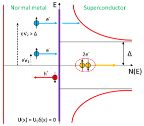
Let us consider a normal metal (N) brought in direct contact with a superconductor (S), with no potential barrier between them. Let’s apply to this junction a voltage being the energy gap in the S side. If the contact is ballistic, the whole voltage drop occurs at the interface. An electron coming from the N side will not be able to propagate through the interface because only Cooper pairs exist in this energy range in S. But if a hole is reflected and two electrons are transmitted in S as a Cooper pair (Fig. 3) the total charge and momentum are conserved. This phenomenon is called Andreev reflection Andreev64 and can be theoretically described by solving the Bogoliubov-de Gennes equations degennes66 at a N/S interface. The reflected hole has opposite wave vector and (if the Cooper pairs are singlets, as in all the cases analyzed here) opposite spin with respect to the incoming electron, so it traces back the trajectory of the incoming electron until a scattering event occurs.
If the applied voltage is much greater than the gap (), all the electrons whose energy is lower that the gap still undergo Andreev reflection, but now their contribution to the current is constant and does no longer depend on the applied voltage. Instead, the electrons with energy higher than the gap are transmitted through the interface (see fig. 3) giving a voltage-dependent current. The total current for is thus blonder83
| (14) |
The second term of the right-hand side of eq. 14 is called “excess current” and is the hallmark of the superconducting state even at energies much higher than the gap. This result is exact only if the gap rises from zero up to the bulk value over a distance larger than the superconducting coherence length . If the gap is instead modeled as a sharp barrier at the interface an additional term equal to must be included.
Because of Andreev reflection, the conductance of the junction turns out to be doubled for . This clearly suggests a simple way to determine the energy gap in the S side by point contact spectroscopy. This technique is often referred to as point-contact Andreev-reflection spectroscopy (PCAR).
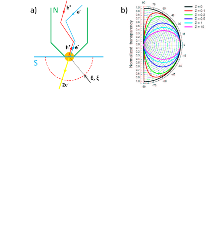
From the solution of the Bogoliubov-de Gennes equations near a interface saint-james64 it is possible to note that Andreev reflection does not occur abruptly at the interface but over a length scale of the order of . In general is also the length over which is depressed due to the proximity effect generated by N on S. However, if the contact size is smaller than this effect can be neglected.
As already mentioned, PCAR requires that the gain in energy of the electrons crossing the junction is well defined. This is true in the ballistic regime but, also, in the diffusive one. If one wants to measure the gap by PCAR, it is clear that the voltage across the junction will reach values of the order of, and even greater than, the gap . If the contact is ballistic, using the value for the carrier density in the free-electron model, it is possible to show deutscher05 that the velocity of electrons across the contact, at , is on the order of the depairing velocity in the superconductor. In other words, the current density becomes overcritical in the contact. Just outside the contact the current spreads out, its density decreases and will reach the critical value a short distance away from the actual junction waldram96 ; daghero06c , as shown in figure 4 (a). If the size of the overcritical region is smaller than the coherence length the spectroscopy is still possible deutscher05 , because superconductivity cannot be quenched over distances smaller than . Therefore it is necessary to adopt contacts (see figure 4 (a)) which are smaller than the electron mean free path (to avoid heating effects) and smaller than the coherence length (to avoid proximity effect and destruction of superconductivity in the contact region) deutscher05 .
IV.2 The Blonder, Thinkam and Klapwijk (BTK) model
Even if Andreev reflection was discovered in the early 60s, it was only in 1982 that Blonder, Thinkam and Klapwijk BTK (from now on referred to as BTK) gave a complete, even though simplified, theoretical discussion of the phenomenon, including the effect of a finite transparency of the interface. The most noticeable simplification is that the model is 1D, i.e. all the involved momenta are normal to the interface and parallel to the axis. The barrier is represented by a repulsive potential located at the interface, which enters in the calculations through the dimensionless parameter
| (15) |
Of course, the smaller is , the more transparent is the barrier. The parameter is originally meant to represent the effect of the typical oxide layer in a point contact, the localized disorder in the neck of a short microbridge or the intentional oxide barrier in a tunnel junction. According to the BTK model, calculated at , the electron coming from the N side can undergo four processes whose probabilities are:
- A
-
probability of Andreev reflection. The probability decreases with increasing for and is always small for ;
- B
-
probability of normal specular reflection. This probability increases with , i.e. on decreasing the barrier transparency;
- C
-
probability of transmission in S as electronlike quasiparticle (ELQ). The probability decreases if increases but it is always zero for ;
- D
-
probability of transmission with FS crossing (i.e. as holelike quasiparticle, HLQ). The probability is small for and always zero for .
Of course the sum of the four probabilities must be equal to 1. Fig.3 shows the particular case of a barrierless () N/S junction at , where only the terms A and C are present.
In can be shown that the expression of the total current across the junction, at T=0, is given by blonder83
| (16) |
where is the Fermi distribution function, and are the coefficients giving the probability of Andreev and ordinary reflection, and the quantity (which is the transmission probability) is often indicated by . Note that, although is formally written only as a function of and , the contribution of an has been taken into account in the calculations. is a constant which depends on the area of the junction, on the density of states and on the Fermi velocity. The derivative of the current with respect to the bias, , provides the conductance of the junction. When divided by the conductance of the same junction when the superconductor is in the normal state, , this gives the normalized conductance of the junction, (which is the outcome of PCAR experiments).
Here, instead of giving the explicit expressions for the probabilities , , and that can be found easily in literature BTK ; deutscher05 ; naidyuklibro , we prefer to show in detail the results of a different approach kashiwaya96 that allows writing the AR normalized conductance at , as a function of the quantities and whose real parts are the BCS quasiparticle and pair density of states, respectively.
We can start from the definition of the transparency of the barrier in the BTK approximation of current injection totally perpendicular to the N/S interface:
| (17) |
and then we introduce the function:
| (18) |
It is trivial to show that:
| (19) |
Note that is a complex function even if the gap is real, as in the BCS case, since and become imaginary for . By using these definitions it is possible to demonstrate that the BTK conductance at is given by:
| (20) |
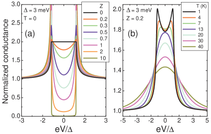
The calculated normalized conductance is shown in Fig. 5(a) for various values of and for 3 meV. In a perfectly transparent junction (, pure Andreev regime) the conductance within the gap () is doubled with respect to the normal-state one. When , two peaks appear at and their amplitude increases on increasing while the zero-bias conductance (ZBC) is depressed. Finally, at , the normalized conductance at coincides with the BCS quasiparticle density of states, i.e. the real part of . Indeed, it can be demonstrated that the results of the BTK model for coincide with the standard results of the theory for NIS (I=insulator) tunnel junctions. Hence, the BTK model can reproduce, by simply changing a parameter, all the different experimental situations corresponding to different transparencies at the N/S interface, from zero to infinity.
Equation 20 is particularly useful to discuss the extensions of the simple BTK formalism we will present in the following sections. As a matter of fact it should be borne in mind that, even if widely used as a simple tool for fitting the experimental PCAR spectra, the original BTK model is based on a large number of approximations and simplifications, i.e.:
-
(1)
All the calculations are made at ;
-
(2)
The problem is 1D, i.e. the current injection is only perpendicular to the plane interface;
-
(3)
The barrier is ideal and presents a null thickness;
-
(4)
The Fermi surfaces of both materials in N and S sides are spherical;
-
(5)
The Fermi velocities are the same in both sides;
-
(6)
The superconductor is supposed homogeneous and isotropic. Because of the mono-dimensionality, the gap entering the equations is actually the gap in one single direction and represents “the” gap only if the order parameter is isotropic (i.e. it has a wave symmetry).
-
(7)
The N/S interface is atomically flat (somehow implicit in the 1D current injection).
In the following we will show that most of these restrictions can be easily relaxed giving a more realistic tool for the analysis of PCAR experiments in a variety of unconventional superconductors.
V Beyond the BTK model
V.0.1 Finite temperature
The calculation of the differential conductance of a N/S junction at finite temperature is a quite easy task. It can be simply accomplished by introducing in the equation for the current the standard convolution with the Fermi function at finite , , and then taking the derivative of the current with respect to the bias voltage, i.e.:
| (21) |
where is given by eq. 20. In figure 5(b) the effect of the thermal broadening on the normalized conductance is calculated by using a temperature-independent gap meV and . At the increase of the two peaks typical of the AR at are smeared out finally leaving a single zero-bias maximum at meV. If the (supposed BCS) temperature dependence of the gap is taken into account in the expressions of and , i.e. in the , the curves become as shown in Fig.6 (b). The AR features now correctly disappear at the critical temperature of the contact (usually equal or very close to the of the superconductor).
The pre-factor of eq.21 is expressed in terms of the normal density of states of the two materials and thus could, at least in principle, depend on temperature and on energy: in this case it should be brought inside the integral, and would no longer simplify when normalizing. This could be the case when the normal state conductance is found experimentally to change with temperature or to be voltage-dependent, as it is in cuprates deutscher05 and in the recently discovered Fe-based superconductors (see sect.VII.3). However, one usually assumes for simplicity that is constant and uses the expression for the normalized conductance to fit the experimental PCAR spectra. From the experimental point of view, however, these cases present the extra problem of defining what is the normal-state conductance to be used for the normalization, as we will show in sect.VII.3.
V.0.2 2D or 3D BTK model
If the current injection was really only perpendicular to the interface as the BTK model assumes, one could in principle probe the k dependence of the gap by making directional PCAR (DPCAR) measurements on the different crystallographic planes of high-quality superconducting single crystals. Actually, charge carriers can approach the interface from any direction and the only condition set by the AR theory is that the component of the k vector parallel to the interface is conserved in all processes. This implies, for example, that the reflected hole comes back in with k opposite to that of the incident electron and traces back its trajectory until the first scattering event in N occurs (see Fig. 4(a)). In the S side a Cooper pair propagates essentially in the same direction as the incident electron (neglecting the small refraction due to the expansion of the FS). Calling the angle between the direction of the incident electron and the normal to the interface, the conservation of transverse momenta leads to the following dependence of the transparency on :
| (22) |
Of course eq.22 coincides with eq.17 for . In figure 4(b) the angular dependence of the normalized transparency (i.e. ) is shown for different values of . When all the quasiparticles are transmitted with the same unitary probability in the whole half-space , but at the increase of the transmission becomes progressively weaker and more directional around the perpendicular to the interface. Strictly speaking, the injection is always in the whole half-space but one can decide to conventionally fix a threshold (e.g. 75 % of the maximum transparency) to determine an equivalent injection angle . In the limit (tunnel regime) one gets , i.e. the tunneling process is certainly highly directional. For the typical values observed in real PCAR experiments (), ranges between and thus evidencing the reduced directionality of the PCAR technique. In addition to these “theoretical” limitations, some practical problems have to be taken into account. Irrespective of the way the PC are realized (needle-anvil or “soft” technique) the contact footprint has a relatively large area (some hundreds of square microns). If this area contains crystal-growth terraces, defects, pits or cracks the probability to have some contacts along a different crystallographic direction becomes high. Directional PCAR (DPCAR) spectroscopy can give reliable results only if very high-quality single crystals with highly regular (and large) surfaces parallel to the crystallographic planes are used. Despite these limitations, we will show in the experimental survey (sect. VII) that recent DPCAR experiments were able to precisely determine the anisotropic properties of the gap in several unconventional superconductors.
As shown in eq. 22 the barrier transparency depends on the direction of the incoming electron in the N side. By introducing this expression in eq.20, integrating over the whole half-plane and properly normalizing, we get the normalized conductance at kashiwaya96 :
| (23) |
The calculation of at any temperature can be done as in eq.21, by a convolution with the Fermi function.
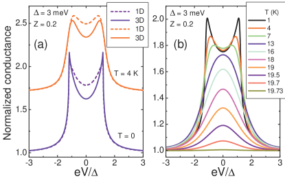
When the system has rotational symmetry around the axis normal to the interface (i.e. the gap is isotropic and the FS is spherical) this approach can be considered as the 3D extension of the BTK model. Figure 6(a) shows the comparison of two normalized conductances at and K calculated with the standard 1D BTK model and with its 3D version. The angular integration leads to a remarkable depression of the AR signal when . Obviously, when (completely transparent junction) or (tunneling regime) the two approaches yield the same results. In figure 6(b) a complete temperature dependency of the normalized conductance calculated by using the 3D model and assuming a BCS dependence is reported. It is trivial to show that the 3D normalized conductance practically coincides with the 1D one calculated for a properly enhanced value. Probably this fact explain why the standard 1D model is still largely used in fitting the experimental data. Nevertheless, problems can arise when comparing the values obtained by the two different approaches, particularly in the cases where the value of has remarkable consequences on the interpretation of the physical process occurring at the interface, as, for example, in the study of ferromagnet-superconductor PCAR junctions.
V.0.3 Fermi velocity mismatch at the interface
In a realistic system the Fermi velocities will be different on the two sides of the contact. The mismatch of the Fermi velocities gives rise to carrier reflections at the interface even when no barrier is present. This effect was initially introduced in the original BTK theory blonder83 by adopting an effective barrier parameter:
| (24) |
where is the ratio of the Fermi velocities in the superconducting and in the normal side. The normal-state resistance at high voltage is given by where is the Sharvin resistance blonder83 .
In the 3D version of the model kashiwaya96 the situation is more complex. To account for the possibility of different effective masses in N and S, the parameter of eq.24 is replaced by . The “refraction” of quasiparticles at the interface is due to the conservation of transverse momentum, i.e. where and are the incidence and transmission angles, respectively. Under these conditions it is possible to show kashiwaya96 that the normal transmission probability (eq. 22) becomes:
| (25) |
By introducing this expression in the formula for the superconducting transmission probability (eq.20) and expressing as a function of by using the “refraction” relation , one formally obtains the same expression for the normalized conductance as in eq. 23 that now, however, accounts for the mismatch in the Fermi velocities. Incidentally, when , i.e. , a “total reflection” of electrons occurs at the interface for injection angles . In this case the integral in has to be restricted to this limit angle kashiwaya96 . It seems that the condition could easily apply in the case of a superconductor with a small or very small FS and, thus, this problem could be important in new unconventional superconductors. In the opposite case, , can vary in the whole half-plane while the range of is restricted. Anyway, whatever the approach to the problem is, it turns out that the global effect of a mismatch of Fermi velocities at the interface is simply described by a sort of “renormalization” of the values of the kind described in eq. 24. As a consequence, apart from extreme and hypothetical cases showing very large (or very small) values, the effect of the mismatch cannot be separated from the standard experimental variability of values, unless one is able to determine the true value at the interface.
V.0.4 The broadening parameter
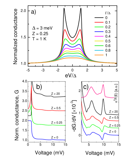
Even if the BTK model allows a correct interpretation of some experiments in low-temperature superconductors blonder83 , in most cases it predicts much sharper gap features than those actually observed in the low-temperature conductance curves. This means that the AR structures in the experimental spectra are not only depressed in amplitude but also spread in energy. This effect can be attributed to the reduction of the quasiparticle lifetime, resulting from: i) the imaginary part of the quasiparticle self-energy. This term is “intrinsic” but very small, as discussed in the tunnel regime by Dynes et al. dynes78 ; ii) inelastic quasiparticle scattering processes occurring near the N/S interface (surface degradation, contamination etc. either at the N or the S side) plecenik94 . This term is “extrinsic” and much larger than the previous one. By properly solving the Bogoliubov-de Gennes equations in the presence of an inelastic scattering term, it has been shown plecenik94 ; srikanth92 that it is possible to globally take these effects into account by including into the BTK model a single broadening parameter in the form of an imaginary part of the energy, i.e. . can thus be considered as the sum of the “intrinsic” lifetime parameter and the “extrinsic” one , being the corresponding intrinsic and extrinsic lifetimes. There is actually a third possible origin of broadening of the conductance curves that can be accounted for by using , i.e. a distribution of gap values (in anisotropic superconductors). In this case, simulates the effect of a convolution of the theoretical conductance with the gap distribution (an example is presented in Sect.VII.4).
Introducing in the BCS quasiparticle density of states leads to the modified expression dynes78 ; plecenik94 :
| (26) |
enters the BTK model or its generalizations through and in eq. 19, thus modifying and the conductance (eq. 23). Fig. 7(a) depicts the normalized conductance calculated using and different values of the ratio . The broadening effect of cannot be reproduced by any combination of parameters of the standard BTK theory unless one convolutes the zero-temperature conductance with the Fermi function at a fictitious temperature higher than the actual one. This approach is sometimes implicitly used indeed when the experimental smearing of the curves is treated in terms of a Gaussian broadening. Such a procedure is not theoretically founded and mixes the actual thermal smearing with the other broadening effects, which are instead well distinct. Finally, even if it is common (and reasonable) opinion that the best conductance curves should allow a fit with , large values might be sometimes necessary (for example in the presence of a wide gap distribution). This does not necessarily prevent the determination of the gap by means of a fitting procedure, which is indeed possible even when (especially if is sufficiently large).
V.0.5 Energy dependence of the order parameter
It is well known that the mean-field BCS definition of a constant superconducting order parameter is only a crude approximation of the physical reality. Actually, even in the weak-coupling regime is a function of the energy and shows a small energy-dependent imaginary part. The signatures of this energy dependence on the normalized tunneling (or AR) conductance curves are extremely small but, when the intensity of the electron-phonon coupling increases (strong-coupling regime) they become visible. By solving the Eliashberg equations for the strong-coupling regime starting from the electron-phonon spectral function and the Coulomb pseudopotential (direct solution) it is possible to obtain the full energy dependence of the order parameter . The imaginary part of increases at the increase of the coupling and accounts for the finite lifetime of Cooper pairs. By introducing the function into the expression for the quasiparticle density of states (eq. 26 with ), small deviations from the BCS DOS at the typical phonon energies are observed, due to the electron-phonon interaction (EPI). It is well known that also the inverse procedure works (but only approximately in multi-band superconductors! dolgov03 ) i.e. starting from the EPI structures in the experimental tunneling conductance it is possible to obtain and by the inverse solution of the Eliashberg equations.
Since the BTK theory (and its modifications discussed so far) coincides with the BCS theory for superconducting tunnel in the limit of large , it is easy to predict that the introduction of into the BTK expressions will lead to EPI structures in the normalized conductance for any value in the ballistic regime. This is indeed the case, as it can be explicitly demonstrated ummarino10 . A simplified approach to the problem was presented in Ref. yanson04c , where simple asymptotic expressions for the normalized conductance at in the tunnel (), ballistic and diffusive regime were obtained by taking into account phonon self-energy effects on the order parameter. Let us instead show here an example of the complete procedure applied to a “classic” strong-coupling superconductor. First, we calculated the function of lead starting from its EPI spectral function (top curve in Fig. 7(c)) and assuming . was thus introduced in the expressions of and finally leading to the point-contact normalized conductance shown in Fig. 7(b) for different values. As expected, the normalized conductance at coincides with the standard BTK one yanson04c . At (where represents the range of energies where ) the EPI structures appear for any value but their amplitude increases with . Fig. 7(c) shows the sign-changed first derivative of the normalized conductance vs. compared to the (top red curve). Even if the EPI structures shift to higher energies and their amplitude is depressed at the decrease of , the use of DPCAR spectroscopy in very high-quality single crystals to access quantitative information on the and its dependence on direction, temperature and applied magnetic fields proved to be a feasible task yanson04c .
V.0.6 Anisotropic order parameter
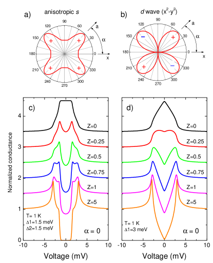
The assumption of an isotropic (-wave) order parameter (OP) makes the BTK model particularly simple, but this constraint must be relaxed if one wants to describe systems in which the OP is instead anisotropic, i.e. it depends on the wavevector in the reciprocal space. This happens for example in high- cuprates, where at least one component of the OP has a -wave symmetry deutscher05 . Generally speaking, the anisotropy of the OP can have two different origins: (i) the OP has a true k dependence (at least along some planes of high symmetry) on the single FS sheet where it opens; (ii) different isotropic OPs open on different sheets of the FS of a multiband system. Strictly speaking, in this case the OP is not anisotropic but appears so when it is measured by techniques with null or poor resolution in the k space. Of course, more complex cases with multiple anisotropic gaps can in principle occur, which could be probably elucidated only by experimental techniques with full k-space resolution (e.g. high-resolution ARPES). In this section, we will show how to account for a single anisotropic OP within the 2D BTK model. The more complex effect of multiple OPs on different FS sheets and the influence of the shape of the FS itself will be addressed in the next section.
The problem of introducing the OP anisotropy into the expression of the superconducting transmission probability was solved in Ref. kashiwaya96 in the most general case. Here we will give a simplified “operative” description of the general results. Let us suppose for simplicity that the OP has a k dependence only in the plane and that is the direction normal to the flat junction interface. Let the system have a translational invariance along the axis so that the problem reduces to a two-dimensional one, i.e. the FS is a cylinder. We also suppose that the current injection occurs in the plane (-plane contact) and that , i.e. there is no refraction of quasiparticles at the interface and both the integration angles and span in the range []. Let the OP be a function of the angle with which electron-like quasiparticles (ELQ) are injected in S. The specific expression of depends on the kind of symmetry the OP shows in the k space. To take into account the possible rotation of the crystallographic axis with respect to the normal to the interface ( axis) we also introduce the angle [see figs. 8(a) and 8(b)]. Since ELQ and HLQ are injected in S with angles and , respectively, they feel different OPs, namely (for ELQ) and (for HLQ). Under these conditions, the superconducting transmission probability becomes kashiwaya96 :
| (27) |
where
and , being the phases of . When are real quantities, then their phase can only be either 0 or and the same holds for . The choice of determines the intervals in which the phase difference is 0 or . If do not show sign changes as a function of , then independently of . appearing in eq.27 has the same expression shown in eq. 25. Putting in eq. 23 one finally obtains the total (integrated) normalized conductance at . The convolution with the Fermi function as in eq.21 will finally give the theoretical curves to be compared with the experimental results at any . Figure 8(c) shows the normalized conductance at K for different values and in the case of anisotropic -wave symmetry of the pair potential, where , ( meV, meV) and . Figure 8(d) shows the normalized conductance for the same values of the parameters in the case of -wave symmetry of the OP, where , ( meV). In both cases the shape of the normalized conductance is quite different from the behavior shown in the -wave case for the same values [figure 5 (a)]. In particular: i) the anisotropic curves show a four-peak (or two-peak and two-shoulder) structure similar to that observed in MgB2 ii) the curve with presents the well-known V-shaped conductance at low bias, while the one with shows a cusp at zero bias instead of the flat region typical of the -wave symmetry. In the -wave symmetry, gives for any value of and the normalized tunneling conductance (for high Z) presents the well-known zero-bias conductance peak deutscher05 .
V.0.7 True shape of the Fermi surfaces and momentum dependence of the pair potential
Taking into account in the calculations for the PCAR conductance the true shape of the Fermi surfaces in N and in S, the possible k dependence of the pair potential and the possible existence of multiple sheets of the FS – where the OP can assume different values – is a rather complicated task, from both the conceptual and the numerical point of view. Let us proceed step by step following the approach reported in mazin99 ; brinkman02 . We will neglect possible interference effects between bands, that can lead to the formation of bound states at the surface as discussed in Ref.golubov09 .
First of all the materials used in the N side are usually good conductors (Au, Ag, Pt, Cu, Al) for which the approximation of a spherical FS is reasonable. So here we restrict the analysis to the shape of the FS in the superconducting material. In the most general case the FS is divided into different sheets. Let us label them with the subscript i and call n the unitary vector in the direction of the total injected current, perpendicular to the contact interface. As a consequence the components along the direction n of the Fermi velocities at wave vector k in the ith FS sheet of the superconductor are where . Of course, due to the previous approximation, the corresponding quantity in the normal metal is , being the (constant in magnitude) Fermi velocity in the normal material. The ith component of the total current flowing through a perfectly transparent () interface with no mismatch of the Fermi velocities () in a ballistic PCAR experiment on a superconductor with isotropic OP is thus mazin99 :
| (28) |
where is the density of states of the ith band at the Fermi energy and wave vector k in S, is the elementary area on the FS in S and is the integral over the ith FS sheet. The integral in eq. 28 is limited to values . Obviously has the meaning of area of the projection of the ith FS sheet along the n direction, i.e. on the interface plane perpendicular to n. It is the area of the ith FS sheet of the superconductor “seen” along the direction n. Of course, under these restrictive conditions every contribution to the total conductance from the ith FS sheet can be evaluated by using the same kind of integral, i.e. is proportional to the projected area . It means that the total conductance “seen” along the direction n is and the total normalized conductance is:
where is the BTK superconducting transmission probability (eq. 20) of the ith FS sheet. In the case of different OPs on the different sheets of the FS the total normalized conductance will be dominated by the contribution of the that corresponds the largest FS projected area along the n direction. As a consequence, directional PCAR experiments at and can give information on the distribution and values of the isotropic OPs on the different FS sheets in a multiband, multigap superconductor. It is quite obvious to expect a similar results also in the more general case of an anisotropic OP and of and , but the calculation of the normalized conductance is now much more complex.
First of all, if the OPs on the FS sheets are anisotropic, i.e. (but still and ), then the superconducting transmission probability becomes a function of and cannot be anymore extracted from the integral over the FS. The total normalized conductance thus becomes:
| (29) |
where is always expressed by eq. 20 but using functions and that substitute the standard ones in the definition of in eq. 19. If the barrier has a finite transparency and there is a N/S Fermi velocity mismatch, the normal transmission probability of the barrier is no longer identically 1. According to the standard 2D extension of the BTK model shown before, (which here we call for simplicity of notation) is given by eq. 25 that can be conveniently rewritten as a function of the projections of the Fermi velocities along the n direction mazin99 :
| (30) |
By introducing this transmission probability inside the integrals over the FS both at numerator and denominator of eq. 29 and taking into account that we finally obtain the total normalized conductance at in the most general case:
| (31) |
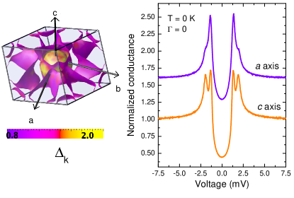
where a subscript has been added to the expressions of and just to include the possibility to have different values along the different crystallographic directions, a thing that is often observed in DPCAR experiments. In the case of large (tunneling regime) the weighting factor inside both the FS integrals of eq. 31 reduces to and the calculations are simplified. As previously, the presence of isotropic OPs on every FS sheet allows extracting from the integrals. This is the approach recently followed by Brinkman et al. in Ref.brinkman02 , where the total normalized conductance of MgB2 has been written as a weighted sum of the partial conductances of the and bands using the squares of the plasma frequencies along the different crystallographic directions as weighting factors. Of course, independently of the isotropic or anisotropic properties of the OPs, if the current injection in a point-contact (or tunneling) experiment was a fully directional process the gap should not be seen along that directions where the FS has a null projected area. Actually, as we have seen in the previous sections, this is not the case, i.e. only a partial directionality is always present, which depends on the and values. This explains why c-axis tunneling experiments on superconductors with a quasi-2D FS (cylinder parallel to ) actually are able to measure the gap averaged over the ab plane. If the gap value and the Fermi velocity are known at any point of the ith FS sheet by first-principle calculations or by high-resolution ARPES experiments, then eq. 31 allows the calculation of the PCAR normalized conductance at for a current injection along any crystallographic direction. An example of the results of this procedure gonnelli08 is shown in Fig. 9, which shows the distribution of the pair potential values over the three different sheets of the FS of CaC6 obtained by first-principle calculations sanna07 (left panel) and the theoretical AR normalized conductance at for current injection along the a axis () and along the c one () (right panel). The theoretical curves of Fig. 9, when properly broadened by values close to the experimental ones, turned out to reproduce very well the experimental DPCAR results in CaC6 gonnelli08 , as it will be shown in Sect.VII.5.
VI Non-ideal effects in the contact
VI.1 Dips
The PCAR differential conductance often shows unexpected sharp dips at voltage values larger than the superconducting gap, but sometimes very close to it, as shown in Fig. 10(a). These dips are related to the superconducting properties of the S electrode since they never show up in NN junctions, but the BTK theory is unable to reproduce them. On increasing temperature, they generally shift to lower energies and generally affect the shape of the gap structures, as shown in Fig.10(a). For example, they can make a broad maximum centered at zero bias look as a sharp zero-bias conductance peak.
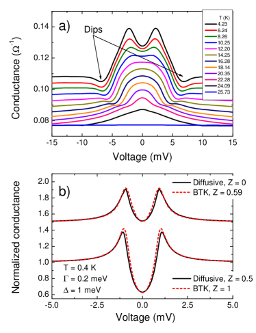
It is commonly accepted that these dips indicate a non-ideal conduction through the contact. The detailed mechanism leading to their emergence was studied by Sheet et al. sheet04 who measured the evolution of the PCAR spectra of various N/S contacts (made with the needle-anvil technique) on progressively reducing the diameter of the point contact by withdrawing the tip in small steps, and found indeed that the dips are related to the regime of conduction through the junction, but also to the bias current. As a matter of fact, according to Wexler’s formula, the point-contact resistance is generally the sum of a Sharvin and a Maxwell contribution, whose relative weight depends on . If is large, the dominant term is the Maxwell one, which contains the bulk resistivity of the two electrodes (eq. 10). As long as the current flowing through the contact is small, the resistivity of the superconductor is zero; however, when the current reaches the critical value () in the S side, a normal-state region can be created in S close to the junction, as discussed in Sect.IV.1. If this happens, the resistivity of the superconductor starts playing a role and enters eq.10, giving a sharp increase in the voltage across the junction and a dip in the differential conductance. The same mechanism can be described as being due to the sudden disappearance of the excess current. Numerical simulations of the conductance, obtained by summing the curves of a ballistic contact (given by BTK) to those of a typical bulk superconductor, give indeed results in good agreement with observations sheet04 .
An alternative explanation of the dips as being due to proximity effect was given in Ref.strijkers01 . The idea is that, if a proximity layer with depressed order parameter is present at the interface, Andreev reflection is limited to energies , while quasiparticles can enter the S side only when . This gives rise to dips in the conductance curves, at energies between and , which also necessarily shift to lower energies on increasing temperature because of the temperature dependence of the gaps. Ref. strijkers01 also provides a model for the fit of the conductance curves that requires , and as adjustable parameters and can be generalized to include a broadening term .
Very often, when analyzing conductance spectra with dips, a BTK fit is done ignoring the dips. However, even if this procedure introduces only a small error in the determination of the gap when the dips are small, it has been shown sheet04 that a considerable overestimation of the gap can occur when they become large.
VI.2 Diffusivity in the contact
In Sect.III.0.3 we mainly discussed the effects of a diffusive contacts in the case of a N/N junction. In N/S junctions, the diffusivity in the contact has been theoretically addressed by Mazin et al. mazin01 ; mazin01b and turns out to affect only the parameter. For instance, the conductance of a diffusive junction with a given barrier parameter can be fitted with a ballistic (BTK) model with an effective . This is shown in figure 10(b) where the conductances obtained within the diffusive model (solid lines) are compared with those calculated with the standard BTK model (dashed lines). All the curves are calculated for meV, meV and K. The upper curves show that the conductance in the diffusive model with is well reproduced by the BTK model with . Analogously, the lower curves indicate that when is introduced in the diffusive model, the obtained conductance corresponds reasonably to that obtained within the BTK model, but with . This conclusion is also, and even more, true at higher temperatures and for higher values of the lifetime broadening, i.e. when the curves are more smeared out.
VI.3 Inelastic scattering in the vicinity of the contact
The inelastic scattering due to some layer with different composition at the N/S interface has been clearly singled out experimentally in ref. chalsani07 where ballistic Andreev-reflection measurements were performed in Cu-Pb junctions with and without a very thin ( nm) Pt layer in between. The PCAR curves of the Cu/Pt/Pb junctions were shown to be more broadened than those of the Cu-Pb contacts, and were well fitted by the BTK model by systematically using larger values – though giving a good determination of the gap amplitude (note that, already in the original paper by Plecenik et al. plecenik94 , was introduced in the BTK model to take into account exactly these effects).
Something similar is likely to happen in the “soft” point contacts, whose normalized conductance curves show a reduced amplitude and a larger broadening than those obtained with the conventional needle-anvil technique. To identify the scattering layer in this case, we carefully measured the temperature dependence of the resistivity of the particular Ag paint used for the contacts. We found a residual resistivity at low temperature of m cm (about times higher than that of pure Ag), and an enormously increased slope of at higher temperature. The former indicates a huge contribution of intergrain connectivity to the resistivity, and the latter a drastic reduction of the inelastic mean free path on the grain surface, which could well give rise to the observed broadening of the conductance curves. It must be said, however, that a contribution from a layer at the surface of the sample cannot be completely ruled out, and is instead proved by the fact that a similar broadening has been observed also in some PCAR spectra taken with the needle-anvil technique. This will be further discussed in the experimental survey (see sections VII.2.1,VII.3).
VI.4 Spreading resistance
For spectroscopic measurements to be reliable, electrons must not lose a significant energy while traveling through the electrodes. If at least one of the electrodes is highly resistive, a so-called spreading resistance must be considered in series with the contact resistance, and this results in a shift of the conductance peaks to higher energies, leading to an overestimation of the gap woods04 ; baltz09 . Actually, a spreading resistance is always present but usually plays a role only in measurements performed in thin films, while in bulk or highly conductive samples it is much smaller than the contact (junction) resistance and can thus be neglected. In the case of “soft” point contacts, one can wonder whether the Ag paste between the Au wire and the sample surface can give a significant contribution to . Actually, the resistance of the Ag-paste spot (approximately modeled as a cylinder with a diameter of 50 m) is as small as 0.086 even if a (largely overestimated) thickness of 50 m is assumed. This value is clearly negligible when compared to the contact resistance that is usually in the range (depending on the material under study).
VII Point-contact spectroscopy in multiband superconductors
VII.1 Two-band model for superconductivity
The first theoretical study of multiband superconductivity dates back to the late Fifties when Suhl, Matthias and Walker suhl59 generalized the BCS theory to the simple case of a superconductor with two overlapping bands. The corresponding BCS Hamiltonian contains two intraband terms of the kind and two interband terms of the kind (where is the band index). is the (constant in the BCS approach) averaged pairing potential which results from boson emission and absorption by an - process, minus the corresponding shielded Coulomb interaction. In the absence of interband coupling (), the two bands would be completely independent, each featuring its own BCS gap and critical temperature. In the opposite case (only interband coupling, ) the critical temperature is the same, but there are still two gaps unless the partial density of states is the same in the two bands (). In general, through interband coupling the band with the higher superconducting raises the critical temperature of the weaker, or even induces superconductivity in a nonsuperconducting band. The critical temperature is defined as where is the effective coupling constant and is simply the maximum eigenvalue of the matrix where is the density of states at the Fermi energy (per spin) in the th band.
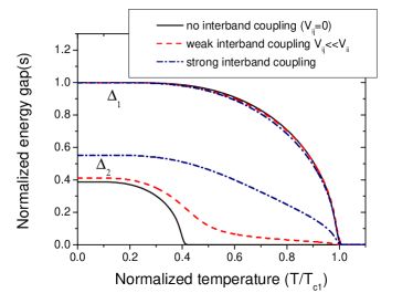
Figure 11 shows the temperature dependence of the (normalized) gaps as a function of the normalized temperature in the BCS two-band model in different cases: i) bands completely decoupled (, solid lines). The ’s of the bands depend on the relevant intraband coupling; ii) weakly coupled bands (dashed lines). While follows the same standard BCS temperature dependence (but with ), features a high-temperature tail and closes at the same as ; iii) strongly coupled bands (dash-dot lines). The small gap still deviates from a BCS-like behavior but smoothly decreases on heating, to finally close rather quickly at . The gap ratios 2 for the two gaps are greater and smaller than the single-band BCS value 3.53, respectively. As we will show in the following experimental survey, PCAR measurements in multiband superconductors have provided examples of all these three cases.
VII.2 Magnesium diboride
After the publication of the theory for two-band superconductivity, some of its consequences on various measurable quantities were calculated and possible marks of multiband superconductivity were found in conventional materials like Nb hafstrom70 ; carlson70 . In 1980 a clearer experimental evidence of multiband superconductivity was found in Nb-doped SrTiO3 binnig80 by means of tunnel spectroscopy. Despite the fundamental importance of the result, the very low transition temperature of this compound (a few hundred mK) made its experimental investigation rather demanding and prevented its study from becoming very popular. The situation changed completely in 2001 when superconductivity below 39 K was discovered in MgB2, which remains up to now the most known and the most studied example of multiband superconductor. MgB2 has a layered structure with graphite-like, honeycomb B layers intercalated by Mg planes with hexagonal close-packed structure buzea01 . Its electronic structure includes four bands originating from -hybrid B orbitals, and two bands due to the overlapping of the residual orbitals. The Fermi surface is made up of nearly-2D cylinders around the line (due to the bands) and a 3D tubular network related to the bands kortus01 . Superconductivity develops in the bands below K mainly because of their coupling to the phonon modes kong01 , and is induced in the bands through interband coupling.
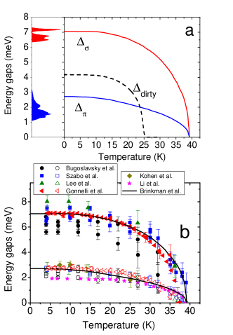
The key role of this two-band-system structure was soon witnessed by the failure of all the conventional single-band theories in describing the phenomenology of MgB2 liu01 ; buzea01 . An effective two-band model was thus proposed, in which the four bands were grouped into two band systems ( and ). The anisotropic effective coupling constant for superconductivity actually indicates an intermediate coupling regime which is best described by the Eliashberg theory eliashberg60 ; choi03 ; nicol05 . The calculation of the gaps within a two-band Eliashberg model brinkman02 gave meV and meV (see Fig.12). Similar values can be obtained within a BCS approach liu01 .
An interesting feature of multiband superconductivity in MgB2 is the role played by impurity scattering in the intraband and interband channels. According to Anderson’s theorem anderson59 , it can be shown golubov97 that, at least for small impurity concentrations, the intraband non-magnetic scattering has no effect on and the gaps. The interband scattering on the other side, has a pair-breaking effect and thus decreases the critical temperature . According to the two-band model, in the limit of very strong interband scattering (dirty limit) a complete isotropization is asymptotically achieved, and the two gaps assume the same value so that one single gap is actually observed (dotted line in Fig.12a). This is often referred to as “gap merging”. According to Eliashberg calculations in Ref.brinkman02 , at low temperature meV with a corresponding reduced K. For the sake of completeness, Fig.12a also shows the results of a fully-anisotropic Eliashberg calculation, based on the actual momentum dependence of the electron-phonon coupling calculated ab-initio choi02 . This approach gives two distinct and non-overlapping distributions of gap values with average meV and meV. The differences from the two-band model arise from details in the calculations that are not worth discussing here. In any case, all calculations show that the gap values on the two band systems are sufficiently different to be distinguishable also experimentally.
According to the discussion of Sect.V.0.7, the shape of the FS (and in particular of the quasi-2D -band sheets) suggests a dependence of the PCAR or tunneling spectra on the direction of (main) current injection. Brinkman et al. brinkman02 calculated the conductance curves of an ideal MgB2-I-N junction with various barrier transparencies within the Eliashberg theory. They expressed the normalized conductance of the junction as the (weighted) sum of the BTK contributions of the two band systems: brinkman02 222In this calculation, interference effects between bands were not taken into account. In a recent paper golubov09 , it has instead been shown that such effects can in principle give rise to observable features in the Andreev conductance spectra not only in iron pnictides, where the order parameter changes sign on different bands, but also in MgB2 where the order parameter has the same sign on both and bands.. As expected, the weight depends on the direction of current injection. For (and parallel to the axis of the nearly cylindrical -band sheets) is no more than 1% so that only the small gap should give detectable structures in the conductance curve. For , is maximum and equal to 33 %, so that four peaks corresponding to the small and the large gaps and are found in the conductance curves brinkman02 . Note that the theoretical values of are referred to ideal tunnelling current injection; slight differences are expected in PCAR experiments where the angle of effective current injection as defined in Sect.V.0.2 can be considerably larger.
VII.2.1 Determination of the gaps in MgB2
The earliest PCAR investigations carried out in MgB2 polycrystals gave evidence of a single isotropic (-wave) gap. Schmidt et al. schmidt01 obtained meV, while Kohen et al. kohen01 measured a gap meV in higher-resistance contacts, while in a lower-resistance junction a smaller gap ( meV) was found, with reduced K. Laube et al.Laube01 obtained an accumulation of gap values around 1.7 meV and 7 meV but never observed both of them in the same spectrum. Plecenik et al.plecenik02 studied the Andreev reflection curves of MgB2/N junctions obtained in different ways, whose fit with the modified BTK model (with meV) gave a gap meV. A discontinuity in the temperature evolution of the gap suggested the existence of parallel contacts in clean and dirty regions of the sample, with a gap meV closing at K and a gap meV closing at K, respectively. The absence of was probably due to a preferred -axis current injection. The presence of a degraded layer on the sample surface suggested in kohen01 and plecenik02 was confirmed by PCAR measurements performed with electrochemically sharpened tips of different hardness gonnelli02a , which showed indeed a decrease in the height of the conductance peaks (from 1.8 down to 1.25) and an increase in from zero up to 1.2 meV on decreasing the pressure in the contact region from about 0.6 GPa down to 0.1 GPa. Spectra taken with the “soft” pressure-less technique had a height of only 1.15, and their fit with a single-gap BTK model gave and meV with a reduced . A reduced was found also in Ref.bugoslavsky02 , together with an increase in and on decreasing the barrier transparency. All these results indicate an extrinsic contribution to from inelastic carrier scattering in the barrier, not easily accountable for in the theoretical model, and possibly due to a degraded or reconstructed layer covering the sample which can be broken by a tip but remains intact when the pressure is small or absent gonnelli02a . Indeed, it was shown experimentally chalsani07 that this effect can be simply accounted for by increasing the broadening parameter(s) in the modified BTK model.
With the improvements in the sample quality, spectra with multiple gap features were readily obtained in films and polycrystals bugoslavsky02 ; szabo01 , that allowed a fit by the two-band BTK model. In principle, the fitting function contains seven parameters: the two gap amplitudes and , the broadening parameters and , two barrier parameters and , plus the weight (so that ) for a total of 7 parameters. Some authors decided to use only one for both bands szabo01 ; bugoslavsky02 but, owing to the different Fermi velocities in the two bands, keeping and as independent parameters is more general. Some authors also take or even replace them with a convolution of the conductance with a Gaussian of width bugoslavsky02 . Others (including us) prefer instead to calculate the conductance at the correct temperature, and add and as imaginary parts of the energy in the BTK equation plecenik94 to account for all the sources of broadening discussed in Sect.V.0.4. Despite the number of free parameters, reliable values of the gaps can be obtained. This is certainly true for which is quite strictly determined by the energy position of the relevant conductance peaks. The same holds for when the relevant peaks are observable – that means, for brinkman02 . When the structures related to the large gap are only smooth shoulders (as in -axis contacts or in -plane contacts at higher temperature), the uncertainty on increases. The evaluation of this uncertainty is not straightforward, because of the complex expression for the conductance in the two-band BTK model and the number of parameters. Indeed, an automated fitting procedure is destined to fail, and one has to manually search for the parameters that allow minimizing the chi-square or the sum of squared residuals (SSR). Once the “best” fit is found, a range of parameters that give “acceptable” fits must be determined. This can be done by fixing a level of confidence for the chi-square or allowing a percent increase in the SSR. Then, the fit has to be repeated many times by changing all the free parameters so as to find the maximum variation of the gaps compatible with the fixed limits. Several fits made independently by different people normally ensure a good estimate of this range. Fortunately, some physical constraints limit the range of variability of some parameters. For example, , and should not depend on either the temperature and the magnetic field; the intrinsic (lifetime) part of and can increase with temperature, but their usually much larger extrinsic part, related to the interface properties, should probably not.
Fig.12(b) reports the experimental results of various PCAR experiments in MgB2. In all cases apart from Ref.li02 a two-band fit was used. All the data sets approximately agree with each other, apart from the early data by Bugoslavsky in thin films which show a reduced . The error bars are indicated only for some data sets and clearly increase on approaching because of the thermal smearing of the gap features. Because of the same effect, one may wonder whether the two gaps really close at the same temperature, since at high temperature the spectra show only a broad maximum and the two-band fit could be questioned. A conclusive answer to this issue and in favor of the two-gap model in MgB2 was found already in 2001 by Szabó et al. szabo01 , who performed PCAR measurements in polycrystalline samples (squares in Fig.12(b)) obtaining gap values in very good agreement with theoretical predictions. They found that the application of magnetic fields to the junctions resulted in a much faster suppression of the -band features with respect to the -band ones. At high temperature or in -axis contacts where no -band features are apparent, the disappearance of the dominant -band structures allows unveiling the underlying -band contribution, with the emergence of two much well resolved maxima related to even at K.
The synthesis of single crystals large enough to be used for PCAR allowed a step forward in the experimental investigation of multiband superconductivity in MgB2, and in particular a study of the anisotropy of the spectra brinkman02 ) by controlling the direction of (main) current injection. The soft-PCAR technique allowed us to make the contacts either on the flat surface of the crystals (-axis contacts in the following, according to the nominal direction of current injection) or on their thin (50-100 m) side (-plane contacts), which is very difficult by using a tip.
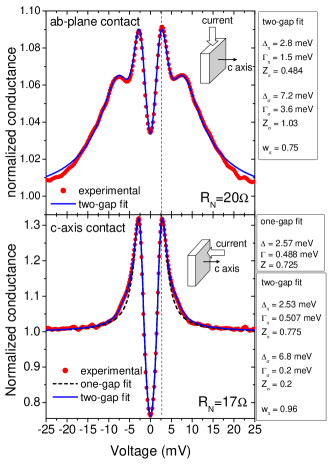
Figure 13 shows two examples of conductance spectra measured in -plane and -axis contacts whose normal-state resistance is indicated in the labels. Note that for all contacts with the rather large mean free path of these samples ( nm) ensures the fulfillment of the conditions for ballistic conduction (see Sect.III.0.1) even if a single contact is hypothesized. Clearly, if several parallel contacts are present, they must be necessarily ballistic gonnelli02c . The spectra are normalized, i.e. divided by the differential conductance at (being the critical temperature of the junction). The experimental curves in Fig.13 clearly show the predicted anisotropy brinkman02 , but the non-perfect directionality of PCAR prevents the weight of the -band conductance from assuming the theoretical extremal values ( for -plane tunneling, for -axis tunneling). This is particularly clear in -axis contacts, where the single-gap BTK fit (dashed line) does not work well and a two-band fit (solid line) is instead necessary (with ). The values of the fitting parameters are indicated in the labels. The temperature dependence of the gaps obtained in different contacts on single crystals gonnelli02c is shown in Fig.12(b) (left triangles).
VII.2.2 PCAR in magnetic field
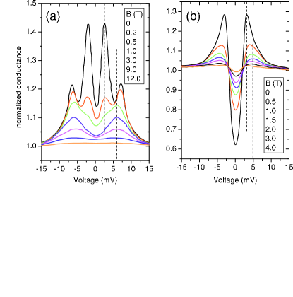
As mentioned above, the first PCAR measurements in MgB2 in the presence of a magnetic field were carried out by Szabó et al. szabo01 in polycrystals. Fig. 14 shows the magnetic field dependence of the low-temperature PCAR spectra for contacts with a large -plane contribution (a) and a dominant -axis contribution (b). In the first case, the peaks related to are fast depressed by weak fields and become barely detectable at T, at which the large-gap maxima are still clearly visible. In the second case, where no clear peaks related to are observed in zero field szabo03b , the suppression of the -gap at 1-1.5 T causes an apparent outward shift of the conductance peaks (from about 3 meV to 5 meV in Fig.14) that then start to shrink, because of the suppression of the -band gap. Actually, the use of polycrystals made it impossible to control the direction of both the probe current and the magnetic field. This is not irrelevant because of the anisotropy of the critical fields in MgB2 sologubenko02 ; welp02 ; angst02 . Indeed, PCAR measurements in single crystals gonnelli02c ; daghero03 ; gonnelli04a showed that: i) A field of about 1 T “completely” suppresses the small gap irrespective of the field direction. This does not mean that the band becomes nonsuperconducting, but simply that above 1 T its contribution to the Andreev signal becomes experimentally undetectable and the conductance curves can be fitted to a function like (where ). Incidentally, this also confirms that the band is rather isotropic; ii) the direction of the field instead affects the behavior of , which is reasonable due to the almost-2D character of this band. When , the peaks in the conductance remain clearly distinguishable up to 9 T, with only some signs of gap closing. Instead, when , they merge together at T giving rise to a broad maximum gonnelli04a ; iii) In any case, at least at 4.2 K, is very little affected by a field of 1 T, either parallel or perpendicular to the ab plane gonnelli02c ; iv) in -axis contacts, the suppression of the -band contribution to the conductance at about 1T is accompanied by an outward shift of the conductance peaks and by an abrupt decrease in the amplitude of the spectrum.
A quantitative study of the effect of the field on the gaps requires a fit of the experimental curves. Here the main problem is: can the BTK model or its generalized version be used to fit the conductance curves when a magnetic field is present? In conventional superconductors, Naidyuk et al. naidyuk96 showed that the pair-breaking effect of the field can be mimicked, within a generalized BTK model, by the broadening parameter . In other words, the total broadening parameter can be considered as the sum of an intrinsic (field-independent) (due to self-energy and inelastic scattering effects, see Sect.V.0.4) and an extrinsic due to the magnetic field. This approach assumes that the pair-breaking effect of the field can be completely represented by the broadening while its effect on the DOS is negligible in a first-order approximation.
Unfortunately, it is not really so. At , the theoretical effects on the DOS curves of both the magnetic field and the actual shape of the FS are very relevant dahm02 ; dahm04a ; koshelev03 so that the BTK model (which in its simplest formulation assumes a spherical FS) even if modified to account for lifetime effects and even if a high is used (tunnel regime), fails in fitting them. One could expect something similar to occur in the AR regime. However, i) the inadequacy of the BTK model is dramatic only at , while at low but finite temperatures (T=4 K) the thermally broadened theoretical DOS curves become much more similar to those given by the standard BTK-lifetime model; ii) as we will show in the following, the model seems to fit much better the experimental curves than the calculated ones, giving results in good agreement with theory. As a matter of fact, the attempts to use the BTK model to obtain the field dependence of the gaps from the conductance curves not only have given good results, but have been able to extract quantitative information about the diffusivities in the two bands gonnelli04a ; bugoslavsky04 ; naidyuk05b . This information is crucial since, as shown in Refs.koshelev03 ; dahm03 ; dahm04a ; gurevich03 , varying the ratio of electron diffusivities in the two bands will change the resulting macroscopic superconducting properties. Incidentally, the possibility to obtain information also on the interband coupling by means of PCAR measurements in the presence of a supercurrent parallel to the interface has been recently proposed Lukic07 .
Figure 15 shows the PCAR spectra of -plane contacts on MgB2 single crystals, in magnetic fields parallel to the axis. The curves of panel (a) were obtained in a “soft” point contact gonnelli04c , while the curves of panel (b) were measured by Naidyuk et al. with a Cu tip naidyuk05b . In both panels, the experimental curves (thick lines) are compared to the two-band generalized BTK fit (thin lines). In panel (a), the fit was carried out with the two-band BTK model up to about 1 T, while above this field the -band features became undetectable so that we took , in agreement with our previous findings in single crystals daghero03 ; gonnelli04a and with those by Szabó et al. In panel (b), instead, the fit was performed with both the and the contributions up to the highest field. A similar result was also obtained by Bugoslavsky et al. in epitaxial thin films of MgB2, where the -band gap was found to survive up to 5 T bugoslavsky04 .
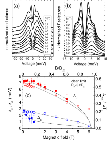
The values of the gaps extracted from the fit are shown in Fig.15(c) as solid and open symbols. The data are compared to the predictions by Dahm et al. dahm04a in the clean limit (solid lines) as well as to those by Koshelev and Golubov koshelev03 in the dirty limit (dashed lines) in the particular case where the diffusivities in the two bands are , which is the case that allows best fitting the data in panel (a). The fit of the experimental PCAR curves seems to work very well and the resulting values of are perfectly compatible with the expected field dependence. In all cases bugoslavsky04 ; gonnelli04c the broadening parameters of the BTK model, and increase linearly with field, giving further support to the distinction between intrinsic lifetime broadening and field-induced broadening (proportional to B).
According to Fig.15(c), a fast suppression of the -band gap features in weak fields szabo01 ; szabo03a ; szabo03b ; gonnelli02c ; daghero03 indicates that the -band diffusivity of the samples under study is a few times greater than the -band one. Since the theoretical field dependence of the gaps in clean limit dahm04a is identical to that predicted by the dirty-limit model in the case (equal diffusivities) koshelev03 , the difference between our results (a) and those by Naidyuk (b) or Bugoslavsky bugoslavsky04 are simply due to sample-dependent variations in the diffusivity ratio , that occurs also in different crystals from the same batch gonnelli04c .
A check of internal consistency of the results described above was achieved by studying the partial averaged zero-bias density of states (ZBD) in the two bands, and , whose magnetic-field dependence is predicted to depend again on the diffusivity ratio koshelev03 . In Ref.gonnelli04c we used the gaps and , the weight and the field-induced broadening parameters obtained from the fit of the PCAR spectra in Fig.15(a) to calculate the zero-temperature ideal tunneling conductance by setting , and . The values of the total ZBD as a function of the magnetic field are shown in Fig.16(a) (symbols), and compared to the theoretical total ZBD were and are those calculated in koshelev03 suitably scaled to the actual critical field T. It is clear that the ZBD follows the theoretical predictions for the case , in perfect agreement with the conclusions drawn from the field dependence of the gaps.
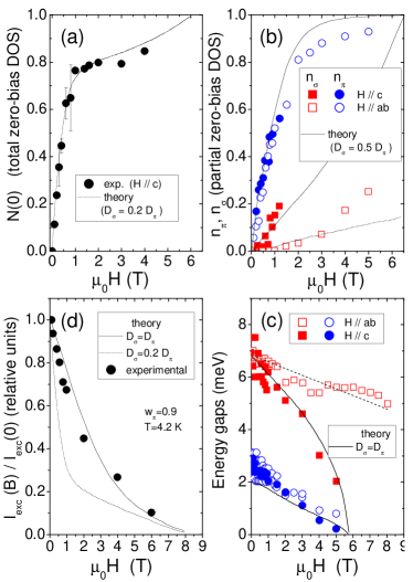
Bugoslavsky et al. bugoslavsky05 were able to directly extract the partial ZBD from the fit of their PCAR spectra in epitaxial MgB2 films with a suitable model developed and tested in conventional type-II superconductors miyoshi05 . The model is based on the existence of parallel contacts and on the fact that a fraction of them (increasing with field) occurs in normal-state regions of the sample (vortex cores) bugoslavsky05 . Hence, what PCAR measures is an effective average over the vortex lattice and the conductance of the point contact should be considered as being the sum of a “normal channel” and of a “superconducting channel” contributions. In MgB2, the normalized conductance in magnetic field thus becomes
| (32) | |||||
where and represent the fraction of normal-state core excitation and were thus identified bugoslavsky05 with the partial ZBD and . To reduce the number of free fitting parameters, the authors assumed and used the convolution with a Gaussian of width to account for both the thermal smearing and inelastic interface scattering. and were fixed to their zero-field values. The values of and obtained from the fit of different series of conductance curves, in magnetic fields either parallel or perpendicular to the axis, are reported in Fig. 16(b). The data in approximately agree with the theoretical curves (solid lines) for . This is consistent with the field dependence of the gaps shown in (c), that shows the persistence of the small gap up to 5 T bugoslavsky04 . Note that the field dependence of and does not depend on the field direction (indicating that the band diffusivity is isotropic) while the -band quantities show a marked anisotropy.
Another interesting way to determine the diffusivity ratio from a PCAR experiment is described in Ref.naidyuk05b , where the excess current – obtained by integration of the reduced after subtraction of the background – is directly plotted as a function of the magnetic field. The result is reported in Fig.16(d) for the curves in Fig.15(b). Let us just recall here for convenience that the excess current is approximately ; when a magnetic field is applied, a fraction of the contact becomes nonsuperconducting (vortex cores) and does not contribute any longer to . Taking into account the presence of two bands (whose partial ZBD behave differently in field) Naidyuk et al. arrived to the expression
| (33) | |||||
that was used to fit the experimental data. In this function, the gaps vales and as well as the ZBD and are taken from the theoretical curves of Ref.koshelev03 suitably scaled to the actual critical field. The zero-field values of the gaps and the weight were obtained from the fit of the zero-field Andreev spectra. Fig.16(d) shows that the experimental values of are in good agreement with the theoretical predictions in the case , which further confirms the conclusion drawn from the magnetic-field dependence of the gaps in Fig.15(c). It is worth mentioning that both in Ref.gonnelli04c and naidyuk05b , different contacts resulted in different values of the diffusivity ratio and the curves shown here are just an example.
The low-temperature magnetic-field dependence of the gaps in single crystals shown in Fig.15(c) indicates that, in these samples, a field of 1 T makes the PCAR spectra look as if the small gap was completely suppressed, but does not seriously affect the -band gap. A fit of the spectra with a function like is thus possible and gives a gap which coincides with the zero-field one – but has a smaller uncertainty because of the reduced number of fitting parameters. If now one subtracts the experimental normalized spectrum from the zero-field one, , one obtains a curve that only contains the zero-field -band contribution and can thus be fitted by a 3-parameters function like from which the small gap can be obtained with a small uncertainty. In this fitting process, all the parameters must be adjusted to ensure a consistency between the different fits. The final result, as shown in Ref.gonnelli02c , is a rather strict determination of the gaps, that turn out to be meV and meV, in excellent agreement with theoretical predictions of Ref.brinkman02 .
The process works well at 4.2 K, and can be extended to higher temperatures with some caution, because of temperature-dependent anisotropy of the critical fields in MgB2 sologubenko02 ; welp02 ; angst02 . In particular, the field must be parallel to the plane daghero03 ; gonnelli04a ; in this case the single-band BTK fit of the PCAR spectra in a field of 1 T (see Fig.17(b)) gives values of that agree very well with those determined by the two-band fit of the zero-field curves (Fig.17(a)) apart from a much smaller uncertainty. The fit of the difference (Fig.17(c)) gives very good results for the small gap as well. The resulting temperature dependence of the gaps gonnelli02c is shown in Fig.17(d).
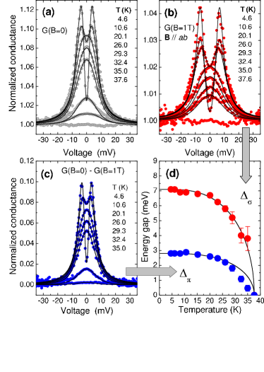
In Refs. gonnelli04a we also determined by means of PCAR the temperature dependence of the critical field , and , identified with the field that suppresses superconductivity and restores the normal-state conductance. For , the critical fields measured by PCAR fall on the curves given by bulk measurements like thermal conductivity sologubenko02 , torque magnetometry angst02 and specific heat welp02 . At lower temperature, they depart from these curves and tend to the (larger) values given by resistivity measurements welp02 ; sologubenko02 . Since the latter rather determine the surface critical field welp02 , some surface effects clearly play a role in PCAR (especially at low temperature). Even if PCS is a surface-sensitive technique, this effect cannot simply be a surface nucleation of superconductivity at a field () because the magnetoresistivity of the electrode is always much lower than that of the MgB2 crystals.
VII.2.3 Determination of the electron-phonon spectral function by PCS
Point contact spectroscopy in the normal and superconducting state of MgB2 was also used to obtain the electron-phonon spectral function and elucidate the role of the in-plane B stretching mode in determining the superconducting properties of this compound. In ref. yanson03 , Yanson et al. investigated the point-contact spectra in -axis oriented films, in the superconducting () and in the normal () state. They directly measured the differential resistance () as well as the second derivative of the I-V curves, i.e. , which is proportional to the electron-phonon spectral function (see Sect.III.0.1). The authors observed clear structures in the superconducting state, with a signature of the mode of the same amplitude as other phonon peaks. Owing to the preferential current injection along the axis, this is in agreement with the calculated golubov02 . However, these structures were found to disappear at where only much smaller nonlinearities persisted. This indicates a superconducting origin of the structures, i.e. due to the energy-dependence of the order parameter (“elastic” or self-energy term) rather than to the actual inelastic e-ph scattering. This point was also addressed theoretically in Ref.yanson04c where a simple asymptotic formula for the order parameter self-energy effects in the superconducting point contact was derived. Later, the same authors performed PCS measurements in single crystals in an inverse needle-anvil configuration (superconducting crystal as the needle) naidyuk03 . The smaller critical field of crystals with respect to films allowed at least a partial suppression of superconductivity at 4.2K by means of fields as high as 9 T. In low-temperature, zero-field spectra with a major contribution from -plane current injection, the second derivative showed a very broad maximum around 60-70 meV that was almost insensitive to magnetic field and was identified with the signature of the phonon mode, largely smeared by the e-ph coupling, as observed by X-ray inelastic scattering shukla03 . The spectra of contacts with a predominant -axis tunneling contribution showed instead much weaker structures such as shallow maxima at 30 and 50 mV that were claimed to reflect bulk (isotropic) phonons, and were put in connection with the first two maxima in the phonon density of states or golubov02 . Further details on this subject can be found in refs. yanson04a and yanson04b .
VII.2.4 Effect of chemical doping on the gaps of MgB2
Chemical substitutions in MgB2 were tried very soon after the discovery of superconductivity in this compound cava03 . The huge experimental work carried out in substituted MgB2 has allowed a deeper understanding of the pure compound, but has also unveiled a surprisingly rich an complex physics. Even in the simplest effective two-band model liu01 ; brinkman02 the quantities needed to describe MgB2 are manifold: four Eliasberg functions (where ) dolgov03 , four quasiparticle scattering rates (intraband, , and interband, ) two densities of states (DOSs), and a prefactor to the Coulomb pseudopotential (which is a 2x2 matrix whose elements only contain the densities of states and ). Not all these parameters are independent (for example , being the zero-bias DOS in the two bands) and some of them (like the DOS, the phonon spectrum) can be either calculated from first principles or determined experimentally. As we will see in the following, chemical doping in MgB2 always gives a decrease in (see Fig.18) and in , that can be due either to a variation in the DOS (and in the phonon frequencies, which however play a minor role) or to an increase in interband scattering. Fortunately, the effects of the latter are rather easily distinguishable from those of other sources of reduction, since an increase in suppresses and but increases . As a consequence, some indications about the effects of doping on the DOS and on the interband scattering can be extracted from the analysis of the doping dependence of the gaps, measured by PCAR, within the two-band Eliashberg theory. Indications about the relative role of intraband scattering rates in the two bands can instead be obtained from the magnetic-field dependence of the ZBD or the excess current, as shown in Sect.VII.2.2. A detailed review about PCAR measurements in doped MgB2 is reported in Ref.gonnelli07 ; in the following we will thus give only a general discussion of the main findings.
In general, a problem with PCAR in doped MgB2 is that the structures related to the large gap become less and less clear on increasing the dopant content. The comparison of the two-band fit to the single-band one can clarify whether two gaps are still present or not, but sometimes the magnetic-field dependence of the conductance curves can be more conclusive in this sense: an outward shift of the conductance peaks is a strong indication in favor of two gaps. Another problem is the determination of the actual doping content, especially in the case of light atomic species (Li, C), which makes the trend of the gaps vs. the doping content rather uncertain. Moreover, the doping content is intrinsically inhomogeneous on the scale probed by PCAR so that different contacts on the same sample can even show different gaps and different . For these reasons, we always prefer to report the values of the gaps as a function of the local critical temperature . This representation is also the most suited to compare the results for different substitutions. For example, one can learn that there is an interesting universal scaling law of with , at least for K, independently of the main mechanism of reduction.
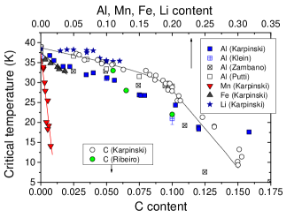
Carbon is the only chemical substitution in the site of boron that the structure of MgB2 accepts. PCAR experiments in Mg(B1-xCx)2 were carried out in nearly single-phase polycrystals with ribeiro03 ; avdeev03 and in single crystals grown at high pressure and high temperature kazakov05 with . The critical temperature decreases on C doping, as shown in Fig.18, although the difficulty in determining the actual C content gives rise to some minor differences in the actual vs. curve for crystals (black circles) and polycrystals (green circles).
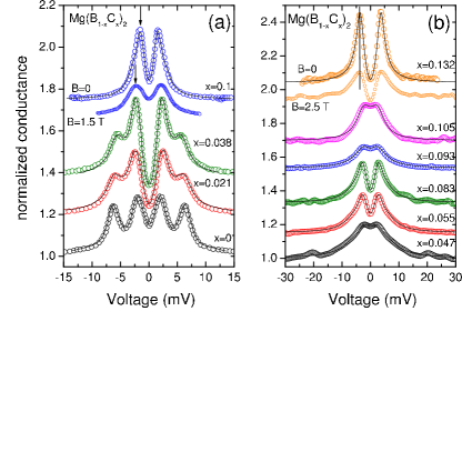
Fig. 19 shows some examples of normalized PCAR curves and the relevant fit at different C contents, in polycrystals and wires holanova04a and in single crystals gonnelli05 . Already at , the experimental curves seem to be fittable by a single-band BTK model with lifetime broadening. Actually, at this C content the second gap is still retained samuely03a as it can be easily shown by applying a magnetic field: as in pure MgB2, the small gap is fast suppressed and the large-gap features emerge clearly holanova04a ; gonnelli05 . As shown in Fig.19(b), in single crystals with the highest doping content () the application of the magnetic field makes the conductance peaks decrease in amplitude but no shift in energy is observed as long as the applied field is much smaller than the critical field (this is certainly true for gonnelli05 because C doping increases the critical field). The absence of a shift indicates that, if two gaps are present, they have very similar amplitude – indeed, the two-band BTK fit of all the conductance curves at requires two gap values that are experimentally indistinguishable. The single-band BTK fit shown in Fig.19(b) gives a gap meV. One could thus conclude that the “gap merging” is obtained in heavily C-doped MgB2, also relying on the fact that: i) the ratio is close to the BCS value; ii) the conductance curves recorded in this sample at different temperatures all admit a very good single-band BTK fit; iii) the temperature dependence of the gap extracted from the fit is perfectly BCS (within the experimental uncertainty) and the critical temperature of the junction, K is in perfect agreement with the bulk measured by DC zero-field-cooling magnetization.
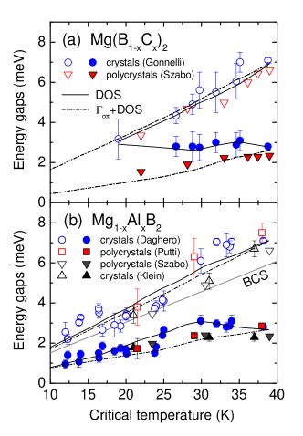
However, the situation is not so simple. Fig. 20(a) reports the values of the gaps obtained in C-doped crystals gonnelli05 and polycrystals holanova04a ; holanova04b ; szabo07 as a function of the critical temperature. It is clear that the two data sets agree rather well as far as is concerned, but disagree on the values and trend of . In particular, in wires and bulk polycrystalline samples there is no tendency to the gap merging observed instead in single crystals. To analyze the data within the two-band Eliashberg model one can use the - and -band DOS and the phonon frequencies calculated for C-doped MgB2 ummarino05a thus leaving and as the only adjustable parameters. The overall trend of the gaps in C-doped polycrystals is reproduced by keeping as in pure MgB2, adjusting to reproduce the experimental , and calculating the corresponding gaps (dashed lines in Fig.20(a)). This means that the decrease in , and in these samples can be completely explained by band filling kortus05 . In single crystals, instead, the trend of can only be reproduced by increasing the interband scattering rate (solid lines in Fig.20(a)). This contrasts with the theoretical prediction erwin03 that substitutions in the B plane (for example by carbon) preserving the different parity of and bands have little or no effect on . The key to this puzzle could be the presence of microscopic defects in C-doped single crystals, acting as scattering centers, suggested by the doing-induced increase in flux pinning and in the normalized resistance kazakov05 . The nature of these defects and the reason why they should be able to create interband scattering is however not completely clear gonnelli05 . It is worth mentioning that the analysis of the zero-bias DOS as a function of the magnetic field in C-doped polycrystals, carried out in ref.szabo07 by using the fitting model developed by Bugoslavsky bugoslavsky05 , clearly proves that the ratio increases from 0.2 (pure MgB2) towards 1 on increasing the doping content, indicating that C doping (surprisingly) increases the intraband scattering more than the -band one.
Doping in the Mg site has been obtained with different chemical species: Al, Li, Mn, Fe. The first two are heterovalent and result in electron and hole doping, respectively. According to theoretical predictions, Al should give the maximum increase in interband scattering (for 2% of Al a value of meV is predicted, which already has measurable effects on the critical temperature and on the gaps erwin03 ). On the contrary, Li should have little or no effect on erwin03 . PCAR measurements in Mg1-xAlxB2 polycrystals putti05 ; szabo07 and crystals klein06 up to , carried out with either the conventional or the “soft” technique, showed an almost linear decrease of and as a function of the Al content, in agreement with the findings of specific-heat measurements putti05 . No clear tendency of the gaps to merge was observed; an extension to higher doping () was later obtained by us in single crystals daghero08 . All these results are reported, as a function of the critical temperature, in Fig.20(b). As in the case of carbon doping, all the data sets agree on the behavior of , which is also directly related to the suppression of the critical field by Al doping putti05 . Interestingly, this relationship implies the validity of a clean-limit description of the system, as it follows from the analysis of the critical field putti05 ; szabo07 but also from the analysis of the zero-bias DOS as a function of the magnetic field (carried out in ref.szabo07 by using Bugoslavsky’s fitting model bugoslavsky05 ) which shows that the diffusivity ratio of pure MgB2 is preserved on Al doping at least up to . The persistence of two gaps even at the highest doping content is not clear in the spectra; the single-band and two-band BTK fit are also very similar to each other although a statistical test (the Fisher F test) clearly indicates that the latter is preferable for any level of confidence. In any case, the magnetic-field dependence of the conductance curves shows the outward shift of the conductance maxima on increasing the field szabo07 ; daghero08 that always indicates the presence of two gaps of different amplitude – even though, as explained in Ref.daghero08 , the suppression of by Al doping prevents the separation of the partial and band contributions to the conductance, as we instead did in pure MgB2.
The dependence of on the critical temperature shown in Fig.20(b) can be superimposed to that observed in C-doped MgB2 szabo07 ; daghero08 shown in Fig.20(a). The trend of the small gap is similar, but not identical, to that observed in C-doped MgB2 polycrystals (see Fig.20(a)). Actually, a small tendency to an increase in at low doping content (with a maximum around K) is very clear, outside the experimental uncertainty, in our data on single crystals (solid circles). Cooley et al. cooley05 noticed the same trend only in samples produced via a long reaction at high temperature so as to reduce the strain and the inhomogeneity in the Al content. This would indicate that the enhancement in is intrinsic to Al doping but is often masked by other effects, and could explain why it is barely detectable in PCAR results by the Slovak group szabo07 ; klein06 (triangles) as well as in the results of specific-heat measurements in some polycrystals samples putti05 ; putti03 . In any case, this trend cannot be reproduced within the two-band Eliashberg model if only the proper variation in the DOS profeta03 and in the phonon frequencies due to Al doping daghero09a are taken into account (dashed lines in Fig.20(b)). Although the effect on the DOS is certainly dominant kortus05 , an increase in interband scattering at low Al contents in quantitative agreement with expectations erwin03 is also necessary to catch the experimental trend of in our single crystals. However, in order to fit the data, must again decrease for . The reason for this is not completely clear but might be related to extrinsic effects like inhomogeneity and lattice stress (not taken into account in the Eliashberg model) that start playing a role for , as suggested in Ref.zambano05 ; cooley05 and by the increase in the width of the superconducting transition for daghero08 .
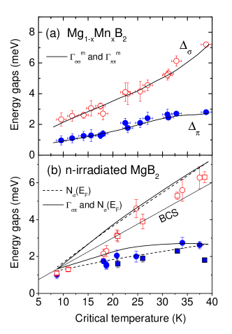
Mn doping is peculiar for two reasons: i) Mn is homovalent with Mg; ii) its magnetic moment gives rise to spin-flip, pair-breaking scattering that is considerably larger than the non-magnetic one: indeed, is very fast suppressed by small Mn contents (see Fig.18). One can thus expect the DOS to be unaffected and the interband non-magnetic scattering to play little role in this compound. PCAR measurements with the soft technique were carried out in single crystals gonnelli06a of Mg1-xMnxB2 with up to 0.015 rogacki06 . The trend of the gaps as a function the is shown in Fig.21(a). For (i.e. for K) the persistence of two gaps was not evident in the conductance curves and had to be proved by using a magnetic field. Unfortunately, Mn doping also suppresses so that, when K, this procedure becomes unreliable and the conclusion that two gaps persist down to the lowest can be based on: i) the better quality of the two-band fit gonnelli06a , and ii) the fact that the presence of a single gap in the low- region would imply a sudden change in the slope of the and vs. curves gonnelli06a that is not justified by any observed discontinuity in the physical properties of the compound rogacki06 . The trend of and vs in Mn-doped MgB2 is surprisingly similar to that observed in Al-doped samples, apart from the low-doping enhancement of . By the way, follows the universal scaling law with . Unlike in previous cases, the analysis of the data within the two-band Eliashberg model can here give precise information on the magnetic scattering rates, either interband () or intraband (). The gap trend can indeed be reproduced very well by using the same phonon spectra, DOS values, and Coulomb pseudopotential as in pure MgB2, neglecting all non-magnetic scattering rates, and taking , and as the only adjustable parameters gonnelli06a . The fit of the gaps vs. indicates a dominant intraband spin-flip scattering in the band, , with possible smaller contributions from either the -intraband or the interband channels. A large scattering was predicted theoretically as being due to the hybridization of the bands of MgB2 with the orbitals of Mn joseph07 . The dominance of this term on the or channels was instead demonstrated by first-principle calculations of the electronic structure of MgB2 near a Mn impurity gonnelli06a .
VII.2.5 Effects of irradiation on the gaps of MgB2
The effects of intentional introduction of disorder in MgB2 by means of neutron irradiation have been recently discussed in a review ferrando07 . Here we will just quickly mention the results of PCAR measurements in neutron-irradiated Mg11B2 polycrystals daghero06c . As explained in tarantini06 , the use of isotopically enriched 11B, was necessary to ensure a homogeneous distribution of defects in the bulk and avoid self-shielding effects. Neutron flux densities up to 1.6 1013 cm-2s-1) were used, which suppressed the bulk down to 8.7 K. The defect distribution is very homogeneous, as shown by X-ray diffraction and by the small width (0.9 K at most) of the superconducting transition tarantini06 . The PCAR measurements were performed with the “soft” technique daghero06c . The severe shortening of the electronic mean free path tarantini06 made fulfilling the conditions for ballistic conduction be more and more difficult. In the most irradiated sample, even the contact with the highest normal-state resistance (40 ) turned out to be in the diffusive regime and showed the typical dips at sheet04 , as well as a moderate heating, which was shown to be negligible as long as the voltage drop at the junction was of the order of daghero06c . The trend of the gaps as a function of is shown in Fig.21(b) (circles). In the region of around 18-19 K, the results of the two-band BTK fit are shown even though a single-band fit (with ) is possible as well. The and curves clearly indicate a transition from two-band to single-band superconductivity below 20 K, in excellent agreement with the findings of specific-heat measurements putti06 in the same samples (squares). The initial small increase in suggests that neutron irradiation increases interband scattering. However, this is not the only effect since a decrease in the -band DOS (indeed observed experimentally gerashenko02 ) is necessary as well to approximately reproduce the overall trend of the gaps within the two-band Eliashberg model (solid line in Fig.21b). Actually, the DOS decrease is dominant and can, alone, qualitatively explain the experimental data (dashed lines) and the inclusion of interband scattering only improves the agreement in the high- region. The fit in the low- region (below 20 K) is poor but cannot be improved since here both gaps are smaller than the BCS value and this is forbidden within the 2-band Eliashberg theory (although often observed in disordered superconductors putti08 ).
VII.3 Point-contact spectroscopy in novel Fe-based superconductors
At the beginning of 2008, a new class of Fe-based superconductors with unexpectedly high critical temperatures – with a record (up to now) of 57 K – was discovered . These materials are the first real term of comparison for cuprates and thus provide a unique opportunity to test the generality of the theories for high- superconductivity and to identify more clearly the conditions for its occurrence. Many compounds of this class have been (and are being) discovered and studied; in the following we will only refer to the most widely studied families of iron-arsenide superconductors. The so called “1111” family includes the compounds REFeAsO (RE= rare earth) that become superconducting upon doping in the O site, with max =55 K as well as the recently discovered oxygen-free Ca1-xRExFeAsF which shows the record = 57 K. The “122” family has general formula AFe2As2 (A=Ba, Sr, Ca, Eu) and, upon doping in the A site, develops up to 38 K. The state of the research on Iron-Pnictide up to May 2009 is (partially) summarized in ref.physicaCFeAs .
Like cuprates, these materials are layered, with alternating RE-O and Fe-As layers, the latter apparently playing the key role for the occurrence of superconductivity. Bandstructure calculations singh08 and ARPES measurements ding08 showed that the Fermi surface is quasi-2D, and is generally made up of two or three hole-like sheets around the point of the first Brillouin zone, and two electron-like cylinders at the M point. This immediately suggests, in analogy with MgB2, the possibility of multigap superconductivity and a dependence of the tunneling or PCAR spectra on the direction of current injection. Experimental indications of multigap superconductivity came very soon from measurements of the critical field and NQR in LaFeAsOF hunte08 ; kohama08 ; kawasaki08 , from direct ARPES measurements in Ba0.6K0.4FeAs ding08 , from NMR in PrFeAsO0.89F0.11 matano08 and so on physicaCFeAs .
The main issue that PCAR spectroscopy has been asked to address is the determination of the number, the amplitude and the symmetry of the order parameter(s). This information is crucial for the development of theoretical models and to test the existing ones.
The first PCAR measurements, carried out with the conventional needle-anvil technique, seemed to support a nodal symmetry of the order parameter, because of the systematic observation of a zero-bias conductance peak (ZBCP). This happened in LaFeAsO0.9F0.1, where Shan et al. shan08 only observed spectra either featureless or with a large ZBCP and much smaller additional features. By fitting the conductance curves with the 2D BTK model kashiwaya96 (see Sects.V.0.2 and V.0.6), they obtained a -wave gap meV, corresponding to . Also Wang et al. wang08 often observed a ZBCP in polycrystalline SmFeAsO0.9F0.1 and interpreted it as a signature of nodal gap. All their spectra admitted a fit with the -wave 2D BTK model, including the few spectra with no ZBCP.
The interpretation of the ZBCP as an indication of nodal symmetry was however soon questioned. Yates et al. yates08a performed PCAR in oxygen-deficient NdFeAsO0.85 with K and observed that a ZBCP (always vanishing at ) develops on increasing the pressure applied by the tip (and thus on decreasing and ). This made the authors warn that the ZBCP may be an artifact, not related to the gap symmetry. A temperature dependence of the ZBCP incompatible with a -wave symmetry was found by the same authors also in TbFeAsO0.9F0.1 with K, where the presence or absence of the ZBCP was found to even depend on the sample region probed by PCAR yates09 . Samuely et al. samuely09a observed, in NdFeAsO0.9F0.1, a large predominance of low-temperature spectra without ZBCP. However, the ZBCP was found to emerge at a temperature , to grow in amplitude until it overwhelms the gap structures (as in yates08a ), and finally to disappear at . A ZBCP very robust against the magnetic field was found in low-resistance junctions by Chen et al. chen08b who performed PCAR measurements in polycrystalline SmFeAsO0.85F0.15 with bulk K. In contrast with ref. shan08 , Chen et al. also found that the ZBCP is very little affected by magnetic fields up to 9T – which excludes its relationship with a -wave symmetry of the gap.
The actual nature of this peak is not completely clear. Kondo scattering coming from the magnetic impurities in or near the barrier shan08 , or to the magnetic moment of Nd or Tb samuely09a ; yates08a , can be excluded. The same holds for intergrain Josephson coupling chen08a . Owing to the decrease in that accompanies the increase in tip pressure, one could hypothesize that the ZBCP is due to the contact not being in the ballistic regime so that critical current effects sheet04 or heating in the contact region occurs. It is true that, as shown in Ref.samuely09a , the ZBCP coexists with clear gap features at finite energy yates08a ; wang08 ; samuely09a , but this does not necessarily exclude the possibility of parallel ballistic and thermal contacts. What instead seems to exclude this picture is that soft point-contact measurements carried out in LaFeAsO1-xFx gonnelli09a ; gonnelli09b and SmFeAsO0.8F0.2 gonnelli09b ; daghero09b never gave evidence of ZBCP irrespective of the contact resistance, which ranged between a few and more than 250 gonnelli09b . Therefore the ZBCP is probably related to the pressure rather than to the contact resistance, and this points towards its relationship with local lattice deformations.
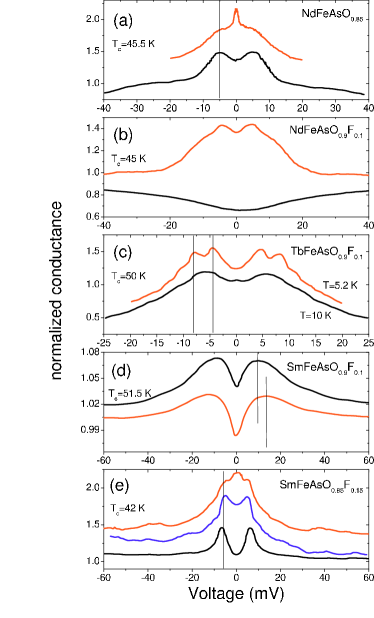
Apart from the zero-bias anomaly, the spectra measured by Yates et al. in NdFeAsO0.85 show conductance maxima in the low-pressure ZBCP-free spectra (bottom curve in Fig.22(a)) which evolve smoothly into shoulders in the high-pressure ones (top curve in Fig.22(a)). The position of these features is robust against pressure and, if taken as an indicator of the gap amplitude, it gives meV corresponding to . A BTK fit (in wave-symmetry) of the bottom spectrum in Fig.22(a) gives meV. In F-doped Nd-1111 (NdFeAsO0.9F0.1) samuely09a , the low-temperature spectra are sometimes featureless (bottom curve in Fig.22(b)) but more often display conductance peaks at mV and shoulders at mV (top curve in Fig.22(b)), which makes them strikingly resemble the PCAR spectra in MgB2. Indeed, they were rather well fitted by a two-band BTK model where being G the normalized junction conductance, and the (unknown) weight of the contribution of band . The best-fitting values of the gaps are meV and meV that, being K, imply gap ratios of 2.6 and 5.7, respectively. Multigap features were clearly observed in Tb-1111 yates09 , in the form of peaks at about and meV (see top curve in Fig.22(c)). The two-band BTK fit of the spectra gave, at low temperature, meV and meV. The PCAR measurements carried out by Wang et al. in polycrystalline SmFeAsO0.9F0.1 gave two distinct families of spectra, with conductance maxima in different positions. Two of them, with no ZBCP, are shown in Fig.22(d). Their fit with a single-band -wave model gave meV and meV wang08 . Similar gap values were given by the two-band -wave fit of the only spectrum with clear two-gap structures (and a ZBCP). However, the spectra shown in Fig.22(d) also admit a two-band BTK fit in -wave. Although the very small amplitude of the signal requires huge values of the broadening parameters, the two -wave gaps meV and meV can be obtained, which are much higher than those given by the single-band -wave fit.
The high-resistance spectra measured by Chen et al. in Sm-1111, showing no ZBCP up to , can be fitted in the whole temperature range with a -wave BTK model. The raw conductance curves reported in Refs.chen08b ; chen09 feature a characteristic left-right asymmetry – also observed in Nd-1111 by Samuely et al. samuely09a and by us in La-1111 gonnelli09a and Sm-1111 daghero09b – probably intrinsic to these materials, as it was in the case of cuprates deutscher05 . The normalized spectra (of which three examples are reported in Fig.22(e)) have very high Andreev signal, always show clear conductance peaks at meV related to a superconducting gap, and often also display additional structures at higher energy that were seen by the authors as extrinsic features and thus disregarded in the fitting procedure. The single-band BTK fit done in chen08b clearly reproduces only the two peaks at about 7 meV and, in the best cases, the zero-bias minimum between them. The resulting gap is very robust against the contact resistance and turns out to be almost perfectly BCS, i.e. meV at low , corresponding to .
The existence of a single BCS gap in iron pnictides is actually surprising since, at the present state of knowledge, there seems to be no possible weak-coupling mechanism able to justify the high of these compounds. The electron-phonon coupling is very weak boeri08 while the coupling mechanisms mediated by spin fluctuations mazin08 proposed for these materials require a strong interband coupling, and are rather unlikely to give the same BCS gap on all the sheets of the Fermi surface. On the other hand, many results, not only from PCAR, speak in favor of a multiband picture. The same spectra measured by Chen et al. may also give indications of multiple gaps, if the additional shoulders at are interpreted as the hallmarks of a larger superconducting gap. This interpretation is questioned by Chen et al. because the position and the amplitude of the additional features are contact-dependent chen09 . This argument holds in conventional superconductors but, for example, it does not in MgB2 (where the observability of the peaks actually depends on the current direction) or in cuprates (where a large spatial inhomogeneity in the gap values has been observed by STM lang02 ).
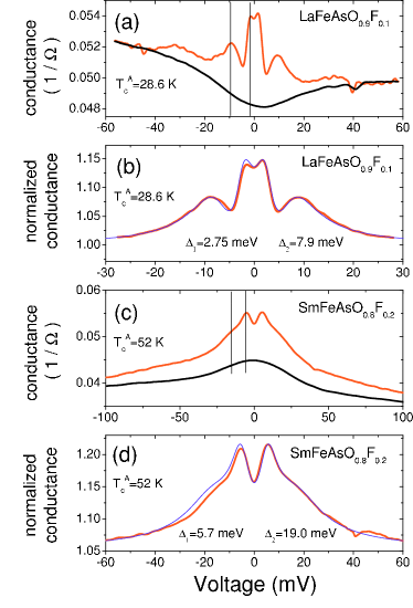
The differential conductance curves measured in “soft” point contacts on SmFeAsO1-xFx polycrystals synthesized at high pressure with ( K) and ( K) daghero09b generally look very similar to those by Chen et al. and always present two clear conductance peaks and additional shoulders that we chose not to disregard in the fit. Similar structures, even more marked, were observed by soft PCAR in LaFeAsO1-xFx polycrystals with bulk K. The normalization of the spectra prior to fitting is complicated by the fact that: i) the normal-state spectrum at low is not accessible due to the high hunte08 ii) the normal state at is not flat but shows a zero-bias hump in Sm-1111 and a pseudogaplike feature in La-1111, both progressively washed out on increasing temperature until, around the Néel temperature of the parent compound (about 140-150 K), the conductance becomes flat (but retains its right-left asymmetry). This suggests that the normal state conductance may change with temperature also below . In the case of Sm-1111, we chose to divide all curves at by the normal state at . In La-1111, we tried different normalizations gonnelli09a and showed that their choice has a small effect on the small gap (less than 2%), while it can change the larger one by about 10% though preserving its trend as a function of temperature, magnetic field and critical temperature. Fig. 23 reports an example of raw conductance curves at low temperature (4.3 K) and at in La-1111 (a) and Sm-1111 (c). The low-temperature normalized curves are shown, together with the relevant two-band BTK fit, in panels (b) and (d). The resulting values of the nodeless gaps are reported in the labels. At least in Sm-1111, the normalized curves still feature an asymmetry that might be due to the normalization (i.e. the asymmetry of the normal state might depend on temperature) or might be an intrinsic feature of these compounds, as it was for cuprates. Certainly, it increases the uncertainty on the gaps ( in particular) since the model can only fit either side of the experimental spectrum (in this case, the right-hand one).
The temperature dependence of the gaps in La-1111 and Sm-1111 gonnelli09a ; gonnelli09b ; daghero09b is reported in Fig.24(a) and (b). In La-1111 (a), three curves are shown, obtained in contacts with different and thus possibly made in regions with different local doping. Note that K corresponds to the very beginning of the resistive transition. At low temperature, the large gap decreases on increasing and apparently disappears at K, while the small gap increases. This finding could be compatible with recent predictions of a doping dependence of the gaps mazin09 ; benfatto08 although any conclusion in this sense is definitely premature. The anomalous dependence of the gaps in La-1111, where seems to close at a above which shows a “tail”, could be due to the shortening of the mean free path on increasing temperature, so that the junction ceases to be ballistic at a voltage that decreases with temperature. This would mean that the superconducting features are progressively weakened starting from the high-bias ones. An indication in this sense is given by the high-temperature curves that are more peaked at zero bias than expected, but if this was the case an apparent decrease in with respect to could be expected, which is instead not observed.
Fig.24(b) shows the gaps values extracted from the fit of various soft-PCAR curves in Sm-1111 gonnelli09b ; daghero09b . Here the situation is clearer: almost coincides with that determined by Chen et al. chen08a (although in our case K while in chen08a K); its values are well reproducible and follow a BCS-like temperature dependence up to . The trend of vs. in each set of data is compatible with a BCS-like curve, but the absolute values are scattered within a region bounded by two BCS-like curves with . This spread could both due to the residual asymmetry of the normalized conductance curves and to the uncertainty introduced by the normalization. The possibility has also been explored theoretically that two large gaps exist, of similar amplitude and thus virtually indistinguishable by PCAR benfatto08 ; ummarino09 . The gaps obtained by fitting Wang’s curves in Fig.22(c) (green circles) with a two-band -wave 2D BTK model turn out to be in agreement with the other results.
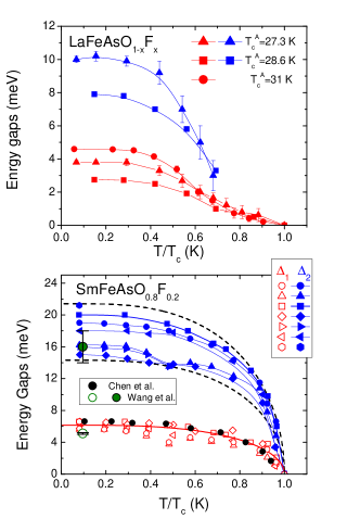
In summary, the interpretation of PCAR spectra in 1111 compounds within a multigap picture gives reasonable results, with a certain degree of universality for the different compounds: i) the low-temperature small gap is a little smaller than BCS in amplitude: ranges between 2.23 and 3.44 in La-1111 gonnelli09a , between 2.54 and 2.95 in Sm-1111 daghero09b and is around 2.1 in Tb-1111 yates09 ; ii) the large gap is larger or much larger than BCS with equal to about 4 in Tb-1111, ranging from 6.42 to 8.68 in La-1111 (when is detectable) and from 6.7 to almost 9 in Sm-1111. Such high values are confirmed, among others, by ARPES measurements in Nd-1111 kondo08 and by infrared ellipsometry in Sm-1111 dubroka09 . They indicate that a non-conventional paring mechanism is taking place – and indeed they can be obtained within the Eliashberg theory ummarino09 by supposing a spin-fluctuation-mediated pairing mechanism related to the nesting of the Fermi surface mazin08 ; benfatto08 and which should give rise to the so-called superconductivity, with nodeless order parameters of opposite sign on the electron-like and hole-like sheets of the Fermi surface. Unfortunately, PCAR in polycrystals cannot give indications about this expected -phase change. A definite answer to the single gap vs. multigap debate could come from ARPES, while phase-sensitive techniques are needed to establish whether the symmetry is really , but probably these developments will need the growth of large enough single crystals. It must be said that preliminary measurements in -plane contacts on Sm-1111 single crystals karpinski09 have perfectly confirmed the results mentioned here daghero09b , supporting the existence of two nodeless gaps.
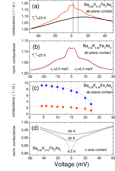
The 122 compounds have been soon grown in the form of large crystals, with markedly layered structure and easily cleavable. ARPES measurements ding08 in (Ba,K)Fe2As2 gave unambiguous evidences of multiple nodeless gaps ( meV on the two small holelike and electron-like FS sheets, and meV on the large hole-like FS). Directional PCAR measurements with a Pt tip were performed in hole-doped Ba0.55K0.45Fe2As2 single crystals by the Slovak group szabo09 ; samuely09b . The majority of -plane point contacts showed a broadened Andreev-reflection feature at zero bias (but no ZBCP) and a pseudogaplike feature in the normal state that persists well above and is very similar to that observed in La-1111 gonnelli09a . As in La-1111, it is not clear whether the contemporaneous observation of superconducting signatures and a pseudogaplike feature means that they spatially coexist or, instead, they belong to spatially separated superconducting and antiferromagnetic phases park09 .
In some contacts, clear double-gap structures were observed, i.e. symmetric peaks at meV and additional shoulders at higher energy (about 10 meV) as in Fig.25(a). In these contacts, the normal-state spectrum at showed a broad hump at zero bias (black curve in Fig.25(a)). The conductance curves were then normalized to the normal-state spectrum and fitted with success to a two-band BTK model, as shown in Fig.25(b). The low-temperature gaps obtained in several contacts are meV and meV, corresponding to gap ratios 2 and 2. Both and were found to follow rather well a BCS-like trend and to close at the same (see Fig.25(c)). The values of these gaps differ from those observed by ARPES in ding08 meV and meV but this difference is partly justified by the different of the samples ( K in Ref.ding08 , K in Ref.szabo09 ).
No trace of gap features were instead observed in -axis contacts (Fig.25(d)), but only a V-shaped conductance progressively flattening on increasing temperature, with no apparent signature of the crossing. The filling effect cannot be simply explained by the thermal broadening of the spectra and continues up to about K, the temperature at which the magnetic transition in the system takes place ni08 .
This marked anisotropy of the spectra is interesting and it is tempting to associate it with an anisotropy of the FS. However, the 122 compounds seem to have a nearly-3D FS vilmercati09 ; mazin09 so that the complete absence of gap signature along the direction is difficult to explain; moreover, as the authors discuss, the inability to observe the gaps in axis contacts might be as well related to surface contamination or reconstruction.
PCAR measurements were also carried out in the electron-doped system with bulk K samuely09b . No multigap features were ever observed in this material; the spectra allowed instead a fit to a standard BTK model, although with large broadening, that gave a single isotropic gap of about 5-6 meV. However, ARPES measurements in the same system ( K) gave evidence of two nodeless gaps meV and meV terashima09 . Evidences of multiple gaps have also been observed in recent (preliminary) soft PCAR measurements in the same material.
VII.4 PCS and PCAR in borocarbides
Since their discovery in 1994, borocarbides with formula (=rare earth, =transition metal, usually Ni) have been the subject of an intensive study. Their crystal structure resembles that of high- cuprates but their electronic properties are rather those of 3D metals. Point contact measurements have been performed in these materials both to determine the electron-boson spectral function (which allows clarifying the nature of the superconducting coupling) and to investigate the symmetry of the superconducting state and/or the possibility of multiband superconductivity.
Among the non-magnetic quaternary borocarbides, is probably the most widely studied. Initially claimed to be a -wave superconductor, it has later been found to display a large anisotropy in the superconducting state but basically isotropic normal-state properties, which suggests an anisotropic order parameter. The proposed symmetries were (or anisotropic -wave), with point nodes in the plane (and precisely along the [100] and [010] directions) and the -wave symmetry, with nodes both in the plane (in the [100] and [010] direction) and along the axis (where instead the gap has a finite value). However, already in 1998, well before the discovery of MgB2, Shulga et al. shulga98 proposed a two-band model to explain the temperature dependence of the critical fields measured in YNi2B2C and LuNi2B2C. As we will see in the following, the debate about the structure and the amplitude of the OP in these compounds is far from being settled, but the multiband scenario is definitely the most supported by the many experimental results.
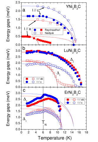
Low- PCS measurements in the normal state of YNi2B2C, obtained by suppressing superconductivity with a magnetic field yanson97 ; naidyuk07a identified a well-resolved maximum in the second derivative at 12 meV that corresponds to a soft phonon mode contributing to about 90% of the total electron-phonon coupling. Other phonon peaks at 20, 24 and 32 meV were not observed. This indicates a superconducting coupling mainly mediated by soft phonons, which usually makes an unconventional gap symmetry rather unlikely. Gap measurements in the superconducting state were carried out by PCAR in single crystals raychaudhuri04 ; mukhopadhyay05 ; naidyuk07a and -axis oriented films bashlakov05 . In single crystals with K Raychaudhuri et al. performed directional PCAR measurements by injecting the current either along the or the axis. Their conductance curves always admitted a single-band BTK fit that however gave clearly different gaps, i.e. a small meV and a much larger meV. The ratio was found to be larger for , possibly indicating (see Sect.V.0.4) a greater angular variation of the gap for -plane contacts, as expected for a symmetry raychaudhuri04 . The temperature dependence of the large gap, which closes at K, was found to slightly deviate from a BCS-like curve (solid circles in Fig.26(a)), which in principle is compatible with a gap with nodes. However, the small gap was found to be fast suppressed on heating, falling below a BCS-like curve with K (dashed line in Fig.26(a)) and to become undetectable above 8 K. The recent measurements of down to 300 mK carried out by the same group and shown in Fig.26(a) (solid squares) indicate that, for K, this gap follows very well a BCS-like curve with . As remarked by the authors raychaudhuri04 , this temperature dependence is inconsistent with a symmetry or with any gap function of the form , and is indeed more compatible with a picture in which the two gaps open on different, weakly coupled bands suhl59 (see Fig.11). The magnetic-field dependence gives similar results mukhopadhyay05 , i.e. the small gap is fast suppressed by the magnetic field and “disappears” well below . This is very similar to what happens in MgB2 when the diffusivities in the two bands are different koshelev03 . Also the zero-bias DOS, calculated by using and taking , increases with field mukhopadhyay05 in a way similar to that predicted by the two-band model for dirty superconductors koshelev03 . If this is the case, the fact that the small gap almost only contributes to the conductance for suggests that it opens on the nearly-cylindrical, fast-electron Fermi surface sheets that have the maximum cross-section (and dominate the conductance) for but play almost no role for mukhopadhyay05 . The multiband picture is also strongly supported by the effect of nonmagnetic (Pt) doping on the critical temperature and the upper critical field mukhopadhyay09 . The decrease of both and (the latter for either orientations of the field, and ) and their subsequent saturation on increasing doping was indeed shown to be explainable, within a two-band picture, as being due to an increase in interband scattering as in doped MgB2 mukhopadhyay09 . Going back to PCAR measurements, further support to the multiband picture also came from the magnetic-field dependence of the excess current obtained by integrating the normalized PCAR spectra in YNi2B2C -oriented films bashlakov05 and single crystals naidyuk07a ; naidyuk07b . As in MgB2 (see Fig.16(d)) shows a positive (although small) curvature. In these measurements, however, the small gap measured by Raychaudhuri et al. was never seen. The conductance curves were found to display only one peak (at either positive or negative bias) and were thus fitted to a single-band BTK model giving a distribution of gap values. In single crystals with K Naidyuk et al. naidyuk07a found for the axis meV, for the axis meV, and for the [110] direction meV. A representative temperature dependence of the gaps for and is shown in Fig.26(a) as open symbols.
In LuNi2B2C single crystals, PCAR measurements carried out by Bobrov et al. bobrov05 gave spectra with a single conductance peak that were however shown to be poorly fitted by a single-band BTK model, and a little better, but still unsatisfactorily, by a two-band one. Two different continuous distributions of gap values were thus used to reproduce the shape of the low-temperature spectra, with ranging between 1 meV to 3.35 meV (with maxima at 2 meV and 3.1 meV) and ranging from 0.7 to 4 meV (with maxima at 1.8-2 meV and 2.5 meV). In bobrov06 ; naidyuk07b , a more conventional two-gap approach was used to fit the data in either direction, although the spectra always featured a single conductance peak – possibly because the two gaps are too close to each other to be clearly distinguishable. As shown in Fig.26(b), a qualitatively similar (but quantitatively different) gap trend as a function of temperature was observed for (squares) and (circles). The results seem to indicate the existence of two bands with a weak, anisotropic interband coupling suhl59 . In a more recent PCAR study in LuNi2B2C single crystals lu08 the spectra were fitted to a single-band BTK model and gave almost equal gaps in the [001] ( axis, meV) and [110] directions ( meV), which clearly excludes a symmetry. Both these gaps approximately follow a BCS-like temperature dependence with equal to 3.4 and 3.6, respectively – although an upward deviation of the experimental points was observed at low temperature, as in films Ref.bobrov05 . These results may be compatible with those by Naidyuk et al. naidyuk07b in the plane, since the single-band fit can reasonably give an “average” gap with respect to the two-band fit and is probably only weakly sensitive to the faster depression of the small gap. Along the axis, a rather wide distribution of gap values meV was observed, all disappearing at the bulk – surprisingly similar to the findings by Bashlakov et al. bashlakov05 in films.
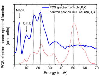
Various other compounds of the family were studied by PCS in the normal state and PCAR, especially by the Ukrainian group, and it would be impossible to account here for all their results. Let us just briefly mention for its interest the magnetic compound with a low-temperature commensurate AFM state whose Néel temperature K is smaller than K. PCS measurements of allowed identifying structures at 16, 22, 34 and 50 meV corresponding to peaks in the phonon DOS of isostructural LuNi2B2C, plus a peak at 3 meV related to the magnetic ordered state and indeed disappearing at , and a peak at 10 meV possibly due to a coupling of carriers to crystal-field excitations yanson97 ; naidyuk07c (see Fig.27). PCAR spectra in the superconducting state first of all showed a negligible dependence on the current direction and admitted single-band BTK fit; the low-temperature gap is meV, and decreases on increasing temperature following a BCS-like curve but disappears at K, well below . Between and , an unconventional gapless state was proposed, possibly due to the peculiar spiral magnetic order in this temperature range. Below , the superconducting state coexists with an antiferromagnetic order. To explain this phenomenon, a separation of the two phases in the space has been proposed. In particular, superconductivity below should survive only on a single (isotropic) sheet of the FS with no contributions from the Ho states. This picture has been directly put in connection with the results of critical field and anisotropy measurements as a function of temperature in the same compound muller07 .
More recently, PCAR measurements have been performed in the compound bobrov08 , with K and a low-temperature incommensurate antiferromagnetic order with spin density wave between 2 K and K. To account for the magnetic pair-breaking effect, a suitable model by Beloborod’ko beloborodko03 was used to fit the spectra. The model contains as adjustable parameters (order parameter, OP), (barrier height) and (magnetic scattering rate). The gap is related to the OP by the formula beloborodko03 . The single-band fit of the PCAR spectra as a function of temperature gave meV for both and . A two-band fit was also carried out because of the claimed unsatisfactory quality of the single-band one. This fit gives two OPs meV and meV whose temperature dependence is shown in Fig.26(c). The anisotropy in this case is small, but a very unconventional behavior is observed because of the AFM order below . The observation of one or two OPs at low temperature clearly proves the coexistence of superconductivity and AFM order, also observed by laser photoemission. On heating, and first increase (possibly because of the weakening of the AFM order), which is consistent with previous findings by tunnel and laser photoemission spectroscopy as well as with the prediction of some theories of coexistence of superconductivity and antiferromagnetic state chi92 . In the paramagnetic state above 6 K, the OPs follow BCS-like curves (whose extrapolation would give K and K) and finally abruptly disappear at K. The extrapolated values give for both OPs a ratio in the strong-coupling regime. To fit the curves, also the weight of the larger OP had to be varied in a non-monotonic way, although it generally decreases on heating. The magnetic scattering rates also evolve non-trivially as a function of temperature, and is always greater than . This results were interpreted as indicating that: i) different bands are differently affected by magnetic order; ii) the part of the FS that develops the larger OP tends to diminish on approaching ; iii) there is a FS separation with distinct superconducting and magnetic bands (or FS sheets); a more detailed analysis of the results in Ref.bobrov08 indicates that approximately half of the FS is nonsuperconducting.
It follows from the above that the result of PCAR measurements in borocarbides carried out by different groups are often in disagreement with one another. Moreover, the coexistence of magnetic orders of some kind and superconductivity in some of this compounds prevents any tentative description of this class of compounds as a whole. Nevertheless, various hints strongly suggest multiband superconductivity, with: i) a conventional phonon-mediated superconducting coupling (at least in non-magnetic ones); ii) weak interband coupling (in raychaudhuri04 ; mukhopadhyay05 and in bobrov06 ; naidyuk07b ) with different gaps and ; iii) a generally anisotropic distribution of gap values over the FS, with a larger gap along the axis; iv) a separation of superconducting and magnetic order parameters on different sheets of the FS (in naidyuk07c and bobrov08 ). The research in this field is still going on and new measurements will certainly help clarifying this complex situation.
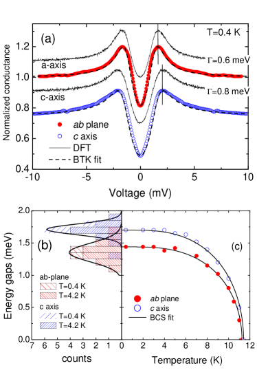
VII.5 PCAR in Graphite-intercalation compounds
The recent discovery of the new superconducting Graphite Intercalation Compounds (GICs) CaC6, YbC6 weller05 , and SrC6 kim07 has renewed the interest for this long-known class of compounds. CaC6 shows the highest K among this class of compounds. Its lattice is made up of alternating graphite layers and Ca planes, with a rhombohedral structure, Emery05 . The similarity with MgB2 is striking and indeed the electronic band structure mazin07 includes the and bands, though the former are completely filled and play no role in superconductivity. According to first-principle calculations calandra05 ; kim06 superconductivity arises from the coupling of both Ca and C phonon modes to the carriers of the so-called interlayer band, which is formed by C and Ca orbitals mazin07 . The Fermi surface mazin07 consists of -band warped cylinders parallel to the axis, and of interlayer-band FS sheets created by the intersection of some of these cylinders with the nearly-spherical Ca orbitals sanna07 . Unlike in MgB2 (see Fig.12(a)) the calculated gap sanna07 is continuously distributed in energy between 1.1 and 2.3 meV and the mixing of C and Ca states prevents a true multigap superconductivity. However, the gap mapping on the FS shows that it changes from one FS sheet to the other and is, on average, slightly larger in the 3D interlayer band (actually depending also on the wavevector within each sheet). This suggested us to use directional soft PCAR in CaC6 single crystals to observe the predicted anisotropy. The extreme sensitivity of CaC6 to air and moisture required to cleave the sample and make the contact in inert atmosphere, and to seal the whole sample holder before transferring it to the cryostat. Due to the small K and the smallness of the effect to be observed, part of the measurements were carried out at 400 mK gonnelli08 .
Fig.28(a) shows a -axis and a -plane PCAR spectrum at K (symbols). The position of the conductance peaks is clearly different and indeed the fit with a single-band 2D BTK model gives meV and meV. The values of are systematically higher in c-axis contacts () than in -plane ones (), in agreement with the different Fermi velocities in the two directions ( m/s, m/s). These spectra are in excellent agrement with ab-initio calculations of the Andreev conductance carried out gonnelli08 as described in Sect.V.0.7, eq.31. To allow a comparison with experiment, the theoretical curves at (shown in Fig. 9) were smeared with the experimental values of (i.e. 0.6 meV for the -plane contact, 0.8 meV for the -axis one) neglecting the (much smaller) thermal smearing. The results are shown in Fig.28 as solid black lines. Fig.28(b) shows that the distributions of low-temperature gap values obtained in several -axis and -plane contacts are approximately Gaussian and overlap only slightly. The temperature dependence of the gaps is shown, for the spectra in Fig.28(a), in panel (c). The gap always follow a BCS-like trend with gap ratio and . All these results gave the first direct evidence of gap anisotropy in CaC6 and showed a very nice example of a successful feedback between PCAR experiments and theoretical predictions from ab-initio calculations.
VIII Conclusions
Multiband superconductivity was theoretically investigated since the Sixties, but it was often considered as an exotic although interesting possibility, with little practical relevance, because of the feebleness of its effects even in the very few cases when they were detected, or the very small critical temperature of the materials that displayed them binnig80 . On the other hand, point-contact spectroscopy was invented in the mid-Seventies and, although initially applied to the study of normal metals, it was soon understood to be a powerful spectroscopic tool in the study of superconductors. However, other techniques such as STM and ARPES with better spatial and momentum resolution largely dominated, in the Nineties, the study of cuprates. With the discovery of MgB2 in 2001, multiband superconductivity suddenly became a promising and popular field of research, and PCAR spectroscopy rapidly acquired a great relevance thanks to its quick and successful application to this compound. The amount of information this technique has been able to provide, even in samples that were impossible to analyze by STM and ARPES, was probably a surprise for most of the superconducting community. Since then, and thanks to its reliability, simplicity and flexibility, PCAR spectroscopy has played an important role in the investigation of the superconducting properties of many new (and less new) compounds.
In this review we have tried to present the recent applications of PCS and PCAR spectroscopy to the study of multiband superconductors, starting from MgB2 (either pure or doped) to continue with borocarbides, graphite-intercalation compounds and the recently discovered Fe-based superconductors. We have shown that PCAR measurements can provide information on the number, the amplitude and the symmetry of the superconducting order parameter(s), but also – when integrated with first-principle calculations and with the Eliashberg theory – on the coupling strengths (both within and between bands), the scattering rates, the densities of states, the dependence of the gap within the various sheets of the Fermi surface, and so on. We have provided the reader with a simple theoretical introduction to PCS and PCAR spectroscopy, showing how the limitations of the original, pioneering Blonder-Tinkham-Klapwijk model (often used even today to fit the point-contact spectra) can be overcome to improve the degree of approximation to the real case and to make PCAR a much sharper tool for the investigation of unconventional superconductors.
Acknowledgments
Our warmest thanks to A. Brinkman, L. Boeri, O. Dolgov, A. Plecenik, P. Raychaudhuri for perusing the manuscript and suggesting corrections and improvements, and to A. Sanna, S. Massidda and P. Raychaudhuri for kindly providing original material. Special thanks to F. Dolcini for helpful discussions on the physics of ballistic contacts. We are indebted to all the members of our group for contributing to the research work summarized here, in particular M. Tortello for experimental research and G.A. Ummarino for theoretical support. A particular acknowledgment to V. A. Stepanov for his fundamental contribution to our research in all these years. R.S.G. wishes to thank R.K. Kremer and the Max Planck Institute für Festkörperforschung (Stuttgart) where this review was partly written.
References
- (1) Yanson I K 1974 Sov. Phys. JETP 39 506–513
- (2) Duif A M, Jansen A G M and Wyder P 1989 J. Phys.: Condens. Matter 1 3157–3189
- (3) Naidyuk Y G and Yanson I K 2004 Point-Contact Spectroscopy (Springer Series in Solid-State Sciences vol 145) (Springer)
- (4) Jansen A G M, van Gelder A P and Wyder P 1980 J. Phys. C: Solid state Phys. 13 6073
- (5) Deutscher G 2005 Rev. Mod. Phys. 77 109
- (6) Blonder G and Tinkham M 1983 Phys. Rev. B 27 112
- (7) Srikanth H and Raychaudhuri A K 1992 Physica C 190 229
- (8) Baltz V, Naylor A D, Seemann K M, Elder W, Sheen S, Westerholt K, Zabel H, Burnell G, Marrows C H and Hickey B J 2009 J. Phys.: Condens. Matter 21 095701
- (9) Holm R 1958 Electric Contacts Handbook (Springer-Verlag)
- (10) Sharvin Y V 1965 Zh. Eksp. Teor. Fiz. 48 984 engl. Transl. Sov. Phys.-JETP 21, 655 (1965)
- (11) de Jong M J M 1994 Phys. Rev. B 49 7778
- (12) Wexler G 1966 Proc. Phys. Soc. London 89 927
- (13) Baranger H U, MacDonald A and Leavens C 1985 Phys. Rev. B 31 6197
- (14) Deutscher G and Maynard R 2002 The Gap Symmetry and Fluctuations in High-Tc Superconductors (NATO Science Series: B vol 371) (Kluwer Academic Publishers) chap From the Andreev Reflection to the Sharvin Contact Conductance, pp 503–510
- (15) Andreev A 1964 Zh. Eksp. Teor. Fiz. 46 1823 engl. Transl. Sov. Phys.-JETP 19, 1228 (1974)
- (16) De Gennes P 1966 Superconductivity of metals and Alloys (Benjamin, New York)
- (17) Saint-James D 1964 J. Phys. 25 899
- (18) Waldram J R 1996 Superconductivity of metals and cuprates (Insitute of Physics Publishing)
- (19) Daghero D, Calzolari A, Ummarino G A, Tortello M, Gonnelli R S, Stepanov V A, Tarantini C, Manfrinetti P and Lehmann E 2006 Phys. Rev. B 74 174519
- (20) Blonder G E, Tinkham M and Klapwijk T M 1982 Phys. Rev. B 25 4515
- (21) Kashiwaya S, Tanaka Y, Koyanagi M and Kajimura K 1996 Phys. Rev. B 53 2667
- (22) Dynes R C, Narayanamurti V and Garno J P 1978 Phys. Rev. Lett. 41 1509
- (23) Plecenik A, Grajcar M, Beňačka v, Seidel P and Pfuch A 1994 Phys. Rev. B 49 10016
- (24) Dolgov O V, Gonnelli R S, Ummarino G A, Golubov A A, Shulga S V and Kortus J 2003 Phys. Rev. B 68 132503
- (25) Ummarino G A In preparation
- (26) Yanson I K, Beloborod’ko S I, Naidyuk Y G, Dolgov O V and Golubov A A 2004 Phys. Rev. B 69 100501
- (27) Mazin I I 1999 Phys. Rev. Lett. 83 1427
- (28) Brinkman A, Golubov A A, Rogalla H, Dolgov O V, Kortus J, Kong Y, Jepsen O and Andersen O K 2002 Phys. Rev. B 65 180517
- (29) Golubov A A, Brinkman A, Tanaka Y, Mazin I I and Dolgov O V 2009 Phys. Rev. Lett. 103 077003
- (30) Gonnelli R S, Daghero D, Delaude D, Tortello M, Ummarino G A, Stepanov V A, Kim J S, Kremer R K, Sanna A, Profeta G and Massidda S 2008 Phys. Rev. Lett. 100 207004
- (31) Sanna A, Profeta G, Floris A, Marini A, Gross E K U and Massidda S 2007 Phys. Rev. B 75 020511(R)
- (32) Sheet G, Mukhopadhyay S and Raychaudhuri P 2004 Phys. Rev. B 69 134507
- (33) Strijkers G J, Ji Y, Yang F Y, Chien C L and Byers J M 2001 Phys. Rev. B 67 104510
- (34) Mazin I I, Golubov A A and Nadgorny B 2001 J. Appl. Phys. 89 7576
- (35) Mazin I, Golubov A A and Nadgorny B 2001 J. Appl. Phys. 90 3127
- (36) Chalsani P, Upadhyay S K, Ozatay O and Burham R 2007 Phys. Rev. B 75 094417
- (37) Woods G T, Soulen R J, Mazin I I, Nadgorny B, Osofsky M S, Sanders J, Srikanth H, Egelhoff W F and Datla R 2004 Phys. Rev. B 70 054416
- (38) Suhl H, Matthias B T and Walker L R 1959 Phys. Rev. Lett. 3 552
- (39) Hafstrom J W and MacVicar M L A 1970 Phys. Rev. B 2 4511
- (40) Carlson J R and Satterthwaite C B 1970 Phys. Rev. Lett. 24 461
- (41) Binnig G, Baratoff A, Hoenig H E and Bednorz J G 1980 Phys. Rev. Lett. 45 1352
- (42) Buzea C and Yamashita T 2001 Supercond. Sci. Technol. 14 R115–R146
- (43) Kortus J, Mazin I I, Belashchenko K D, Antropov V A and Boyer L L 2001 Phys. Rev. Lett. 86 4656
- (44) Kong Y, Dolgov O V, Jepsen O and Andersen O K 2001 Phys. Rev. B 64 020501(R)
- (45) Liu A Y, Mazin I I and Kortus J 2001 Phys. Rev. Lett. 87 87005
- (46) Eliashberg G M 1960 Sov. Phys. JETP 11 696
- (47) Choi H J, Cohen M L and Louie S G 2003 Physica C 385 66–74
- (48) Nicol E and Carbotte J P 2005 Phys. Rev. B 71 054501
- (49) Anderson P W 1959 J. Phys. Chem. Solids 11 26
- (50) Golubov A A and Mazin I I 1997 Phys. Rev. B 55 15146
- (51) Choi H J, Roundy D, Sun H, Cohen M L and Louie S G 2002 Nature 418 758–760
- (52) Bugoslavsky Y, Miyoshi Y, Perkins G K, Berenov A V, Lockman Z, MacManus-Driscoll J L, Cohen L F, Caplin A D, Zhai H Y, Paranthaman M P, M C H and Blamire M 2002 Supercond. Sci. Technol. 15 526
- (53) Szabó P, Samuely P, Kacmarcik J, Klein T, Marcus J, Fruchart D, Miraglia S, Marcenat C and Jansen A G M 2001 Phys. Rev. Lett. 87 137005
- (54) Lee S, Khim Z G, Chong Y, Moon S H, Lee H N, Kim H G, Oh B and Jip Choi E 2002 Physica C 377 202
- (55) Gonnelli R S, Daghero D, Ummarino G A, Stepanov V A, Jun J, Kazakov S M and Karpinski J 2002 Phys. Rev. Lett. 89 247004
- (56) Kohen A and Deutscher G 2001 Phys. Rev. B 64 060506
- (57) Li Z Z, Tao H J, Xuan Y, Ren Z A, Che G C and Zhao B R 2002 Phys. Rev. B 66 064513
- (58) Schmidt H, Zasadzinski J F, Gray K E and Hinks D G 2001 Phys. Rev. B 63 220504
- (59) Laube F, Goll G, Hagel J, Löhneysen H V, Ernst D and Wolf T 2001 Europhysics Letters 56 296
- (60) Plecenik A, Benacka S, Kus P and Grajcar M 2002 Physica C 368 251
- (61) Gonnelli R S, Calzolari A, Daghero D, Ummarino G A, Stepanov V A, Fino P, Giunchi G, Ceresara S and Ripamonti G 2002 J. Phys. Chem. Solids 63 2319
- (62) Szabó P, Samuely P, Kacmarcik J, Jansen A G M, Klein T, Marcus J and Marcenat C 2003 Supercond. Sci. Technol. 16 162
- (63) Sologubenko A, Jun J, Kazakov S M, Karpinski J and Ott H R 2002 Phys. Rev. B 66 014504
- (64) Welp U, Rydh A, Karapetrov G, Kwok W K, Crabtree G W, Marcenat C, Paulius L, Klein T, Marcus J, Kim K H P, Jung C U, Lee H S, Kang B and Lee S I 2003 Phys. Rev. B 67 012505
- (65) Angst M, Puzniak R, Wisniewski A, Jun J, Kazakov S M, Karpinski J, Roos J and Keller H 2002 Phys. Rev. Lett. 88 167004
- (66) Daghero D, Gonnelli R S, Ummarino G A, Stepanov V A, Jun J, Kazakov S M and Karpinski J 2003 Physica C 385 255
- (67) Gonnelli R S, Daghero D, Ummarino G A, Dellarocca V, Calzolari A, Stepanov V A, Jun J, Kazakov S M and Karpinski J 2004 Physica C 408-410 796
- (68) Naidyuk Y G, Häussler R and Löhneysen H v 1996 Physica B 218 122
- (69) Dahm T, Graser S, Iniotakis C and Schopohl N 2002 Phys. Rev. B 66 144515
- (70) Dahm T, Graser S and Schopohl N 2004 Physica C 408-410 336
- (71) Koshelev A E and Golubov A A 2003 Phys. Rev. Lett. 90 177002
- (72) Bugoslavsky Y, Miyoshi Y, Perkins G K, Caplin A D, Cohen L F, Pogrebnyakov A V and Xi X X 2004 Phys. Rev. B 69 132508
- (73) Naidyuk Y G, Kvitnitskaya O E, Yanson I K, Leeb S and Tajima S 2005 Solid State Communications 133 363
- (74) Dahm T and Schopohl N 2003 Phys. Rev. Lett. 91 017001
- (75) Gurevich A 2003 Phys. Rev. B 67 184515
- (76) Lukic V and Nicol E J 2007 Phys. Rev. B 76 144508
- (77) Gonnelli R S, Daghero D, Calzolari A, Ummarino G A, Dellarocca V, Stepanov V A, Jun J, Kazakov S M and Karpinski J 2004 Phys. Rev. B 69 100504(R)
- (78) Szabó P, Samuely P, Kacmarcik J, Klein T, Marcus J and Jansen A G M 2003 Physica C 388-389 145
- (79) Bugoslavsky Y, Miyoshi Y, Perkins G K, Caplin A D, Cohen L F, Pogrebnyakov A V and Xi X X 2005 Phys. Rev. B 72 224506
- (80) Miyoshi Y, Bugoslavsky Y and Cohen L F 2005 Phys. Rev. B 72 012502
- (81) Gonnelli R S, Daghero D, Ummarino G A, Stepanov V A, Jun J, Kazakov S M and Karpinski J 2003 Supercond. Sci. Technol. 16 171
- (82) Yanson I K, Fisun V V, Bobrov N L, Naidyuk Y G, Kang W N, Choi E M, Kim H J and Lee S I 2003 Phys. Rev. B 67 024517
- (83) Golubov A A, Kortus J, Dolgov O V, Jepsen O, Kong Y, Andersen O K, Gibson B J, Ahn K and Kremer R K 2002 J. Phys.: condens. matter 14 1353
- (84) Naidyuk Y G, Yanson I K, Kvitnitskaya O E, Lee S and Tajima S 2003 Phys. Rev. Lett. 90 197001
- (85) Shukla A, Calandra M, d Astuto M, Lazzeri M, Mauri F, Bellin C, Krish M, Karpinski J, Kazakov S M, Jun J, Daghero D and Parlinski K 2003 Phys. Rev. Lett. 90 095506
- (86) Yanson I K and Naidyuk Y G 2004 Low Temp. Phys. 30 261
- (87) Yanson I K and Naidyuk Y G 2004 Spectroscopy of Emerging Materials (NATO Science Series II: Mathematics, Physics and Chemistry vol 165) (Kluwer Academic Publisher) chap Point-contact spectroscopy of two-band superconductor , p 273
- (88) Cava R J, Zandbergen H W and Inumaru K 2003 Physica C 385 8–15
- (89) Gonnelli R S, Daghero D, Ummarino G A, Tortello M, Delaude D, Stepanov V A and Karpinski J 2007 Physica C 456 134
- (90) Ribeiro R, Bud ko S, Petrovic C and Canfield P 2003 Physica C 384 227
- (91) Klein T, Lyard L, Marcus J, Marcenat C, Szabó P, Hol’anová Z, Samuely P, Kang B W, Kim H J, Lee H S, Lee H K and Lee S I 2006 Phys. Rev. B 73 224528
- (92) Zambano A J, Moodenbaugh A R and Cooley L D 2005 Supercond. Sci. Technol. 18 1411–1420
- (93) Putti M, Ferdeghini C, Monni M, Pellecchi I, Tarantini C, Manfrinetti P, Palenzona A, Daghero D, Gonnelli R S and Stepanov V A 2005 Phys. Rev. B 71 144505
- (94) Karpinski J, Zhigadlo N D, Katrych S, Puzniak R, Rogacki K and Gonnelli R 2007 Physica C 456 3
- (95) Avdeev M, Jorgensen J D, Ribeiro R A, Bud ko S L and Canfield P C 2003 Physica C 387 301
- (96) Kazakov S M, Puzniak R, Rogacki K, Mironov A V, Zhigadlo N D, Jun J, Soltmann C, Batlogg B and Karpinski J 2005 Phys. Rev. B 71 024533
- (97) Holanová Z, Szabò P, Samuely P, Wilke R H T, Bud’ko S L and Canfield P C 2004 Phys. Rev. B 70 064520
- (98) Gonnelli R S, Daghero D, Calzolari A, Ummarino G A, Dellarocca V, Stepanov V A, Kazakov S M, Zhigadlo N and Karpinski J 2005 Phys. Rev. B 71 060503R
- (99) Samuely P, Hol’anovà Z, Szabò P, Kacmarcik J, Ribeiro R A, Bud’ko S L and Canfield P C 2003 Phys. Rev. B 68 020505(R)
- (100) Holanová Z, Szabó P, Kacmarcik J, Samuely P, Ribeiro R A, Bud’Ko S L and Canfield P C 2004 Physica C 408-410 610
- (101) Szabó P, Samuely P, Pribulová Z, Angst M, Bud’ko S, Canfield P C and Marcus J 2007 Phys. Rev. B 75 144507
- (102) Daghero D, Delaude D, Calzolari A, Tortello M, Ummarino G A, Gonnelli R S, Stepanov V A, Zhigadlo N D, Katrych S and Karpinski J 2008 J. Phys.: Condens. Matter 20 085225
- (103) Ummarino G A, Daghero D, Gonnelli R S and Moudden A H 2005 Phys. Rev. B 71 134511
- (104) Kortus J, Dolgov O V, Kremer R K and Golubov A A 2005 Phys. Rev. Lett. 94 027002
- (105) Erwin S C and Mazin I I 2003 Phys. Rev. B 68 132505
- (106) Cooley L D, Zambano A J, Moodenbaugh A R, Klie R F, Zheng J C and Zhu Y 2005 Phys. Rev. Lett. 95 267002
- (107) Putti M, Affronte M, Manfrinetti P and Palenzona A 2003 Phys. Rev. B 68 094514
- (108) Profeta G, Continenza A and Massidda S 2003 Phys. Rev. B 68 144508
- (109) Daghero D Ummarino G A, Tortello M, Delaude D, Gonnelli R S, Stepanov V A, Monni M and Palenzona A 2009 Supercond. Sci. Technol. 22 025012
- (110) Gonnelli R S, Daghero D, Ummarino G A, Calzolari A, Tortello M, Stepanov V A, Zhigadlo N D, Rogacki K, Karpinski J, Bernardini F and Massidda S 2006 Phys. Rev. Lett. 97 037001
- (111) Putti M, Affronte M, Ferdeghini C, Manfrinetti P, Tarantini C and Lehmann E 2006 Phys. Rev. Lett. 96 077003
- (112) Rogacki K, Batlogg B, Karpinski J, Zhigadlo N D, Schuck G, Kazakov S M, Wägli P, Puźniak R, Wiśniewski A, Carbone F, Brinkman A and van der Marel D 2006 Phys. Rev. B 73 174520
- (113) Joseph P J T and Singh P P 2007 Solid State Commun. 141 390
- (114) Ferrando V, Affronte M, Daghero D, Di Capua R, Tarantini C and Putti M 2007 Physica C 456 144
- (115) Tarantini C, Aebersold H U, Braccini V, Celentano G, Ferdeghini C, Ferrando V, Gambardella U, Gatti F, Lehmann E, Manfrinetti P, Marré D, Palenzona A, Pallecchi I, Sheikin I, Siri A S and Putti M 2006 Phys. Rev. B 73 134518
- (116) Gerashenko A P, Mikhalev K N, Verkhovskii S V, Karkin A E and Goshchitskii B N 2002 Phys. Rev. B 65 132506
- (117) Putti M, Vaglio R and Rowell J M 2008 Supercond. Sci. Technol. 21 043001
- (118) 2009 Physica C. Special Issue: Superconductivity in Iron Pnictides 469
- (119) Singh D J and Du M H 2008 Phys. Rev. Lett. 100 237003
- (120) Ding H, Richard P, Nakayama K, Sugawara K, Arakane T, Sekiba Y, Takayama A, Souma S, Sato T, Takahashi T, Wang Z, Dai X, Fang Z, Chen G F, Luo J L and Wang N L 2008 Europhys. Lett. 83 47001
- (121) Hunte F, Jaroszynski J, Gurevich A, Larbalestier D C, Jin R, Sefat A S, McGuire M A, Sales B C, Christen D K and Mandrus D 2008 Nature (London) 453 903
- (122) Kohama Y, Kamihara Y, Riggs S, Balakirev F F, Atake T, Jaime M, Hirano M and Hosono H 2008 Europhys. Letters 84 37005
- (123) Kawasaki S, Shimada K, Chen G F, Luo J L, Wang N L and Zheng G q 2008 Phys. Rev. B 78 220506(R)
- (124) Matano K, Ren Z A, Dong X L, Sun L L, Zhao Z X and Zheng G q 2008 Europhys. Lett. 83 57001
- (125) Shan L, Wang Y, Zhu X, Mu G, Fang L, Ren C and Wen H H 2004 Europhys. Lett. 83 57004
- (126) Wang Y L, Shan L, Fang L, Cheng P, Ren C and Wen H H 2009 Supercond. Sci. Technol. 22 015018
- (127) Yates K A, Cohen L F, Ren Z A, Yang J, Lu W, Dong X L and Zhao Z X 2008 Supercond. Sci. Technol. 21 092003
- (128) Yates K A, Morrison K, Rodgers J A, Penny G B S, Bos J W G, Attfield J P and Cohen L 2009 New J. Phys. 11 025015
- (129) Samuely P, Szabó P, Pribulová Z, Tillman M, Bud’ko S L and Canfield P C 2009 Supercond. Sci. Technol. 22 014003
- (130) Chen T Y, Tesanovic Z, Liu R H, Chen X H and Chien C L 2008 Nature (London) 453 761
- (131) Chen X H, Wu T, Wu G, Liu R H, Chen H and Fang D F 2008 Nature (London) 453 1224
- (132) Gonnelli R S, Daghero D, Tortello M, Ummarino G A, Stepanov V A, Kim J S and Kremer R K 2009 Phys. Rev. B 79 184526
- (133) Gonnelli R S, Daghero D, Tortello M, Ummarino G A, Stepanov V A, Kim J S and Kremer R K 2009 Physica C 469 512
- (134) Daghero D, Tortello M, Gonnelli R S, Stepanov V A, Zhigadlo N D and Karpinski J 2009 Phys. Rev. B 80 060502(R)
- (135) Chen T Y, Huang S X, Tesanovic Z, Liu R H, Chen X H and Chien C L 2009 Physica C 469 521
- (136) Boeri L, Dolgov O V and Golubov A A 2008 Phys. Rev. Lett. 101 026403
- (137) Mazin I I, Singh D J, Johannes M D and Du M H 2008 Phys. Rev. Lett. 101 057003
- (138) Lang K M, Madhavan V, Hoffman J E, Hudson E W, Eisaki H, Uchida S and Davis J C 2002 Nature (London) 415 412
- (139) Mazin I I and Schmalian J 2009 Physica C 469 614
- (140) Benfatto L, Capone M, Caprara S, Castellani C and Di Castro C 2008 Phys. Rev. B 78 140502(R)
- (141) Ummarino G A, Tortello M, Daghero D and Gonnelli R S 2009 Phys. Rev. B 80 in press
- (142) Kondo T, Santander-Syro A F, Copie O, Liu C, Tillman M E, Mun E D, Schmalian J, Bud’ko S L, Tanatar M A, Canfield P C and Kaminski A 2008 Phys. Rev. Lett 101 147003
- (143) Dubroka A, Kim K W, Rössle M, Malik V K, Drew A J, Liu R H, Wu G, Chen X H and Bernhard C 2008 Phys. Rev. Lett. 101 097011
- (144) Karpinski J, Zhigadlo N, Katrych S, Bukowski Z, Moll P, Weyeneth S, Keller H, Puzniak R, Tortello M, Daghero D, Gonnelli R S, Maggio-Aprile I, Fasano Y, Fischer Ø, Rogacki K and Batlogg B 2009 Physica C 469 370
- (145) Szabó P, Pribulová Z, Pristáš G, Bud’ko S L, Canfield P C and Samuely P 2009 Phys. Rev. B 79 012503
- (146) Samuely P, Pribulová Z, Szabó P, Pristáš G, Bud’ko S L and Canfield P C 2009 Physica C 469 507
- (147) Park J T, Inosov D S, Niedermayer C, Sun G L, Haug D, Christensen N B, Dinnebier R, Boris A V, Drew A J, Schulz L, Shapoval T, Wolff U, Neu V, Yang X, Lin C T, Keimer B and Hinkov V 2009 Phys. Rev. Lett. 102 117006
- (148) Ni N, Bud’ko S L, Kreyssig A, Nandi S, Rustan G E, Goldman A I, Gupta S, Corbett J D, Kracher A and Canfield P C 2008 Phys. Rev. B 78 014507
- (149) Vilmercati P, Fedorov A, Vobornik I, Manju U, Panaccione G, Goldoni A, Sefat A S, McGuire M A, Sales B C, Jin R, Mandrus D, Singh D J and Mannella N 2009 Phys. Rev. B 79 220503
- (150) Terashima K, Bowen J H, Nakayama K, Sato T, Richard P, Xu Y M, Li L J, Cao G H, Xu Z A, Ding H and Takahashi T 2009 Proc. Natl. Acad. Sci (USA) 106 7330
- (151) Shulga S V, Drechsler S L, Fuchs G, Müller K H, Winzer K, Heinecke M and Krug K 1998 Phys. Rev. Lett. 80 1730
- (152) Naidyuk Y G, Bashlakov D L, Yanson I K, Fuchs G, Behr G, Souptel D and Drechsler S L 2007 Physica C 460-462 103
- (153) Raychaudhuri P, Jaiswal-Nagar D, Sheet G, Ramakrishnan S and Takeya H 2004 Phys. rev. Lett. 93 156802
- (154) Naidyuk Y G, Bashlakov D L, Bobrov N L, Chernobay V N, Kvitnitskaya O E, Yanson I K, Behr G, Drechsler S L, Fuchs G, Souptel D, Naugle D G, Rathnayaka K D D and Ross J H 2007 Physica C 460-462 107
- (155) Bobrov N L, Chernobay V N, Naidyuk Y G, Tyutrina L V, Naugle D G, Rathnayaka K D D, Bud’ko S L, Canfield P C and Yanson I K 2008 Europhys. Lett. 83 37003
- (156) Yanson I K, Fisun V V, Jansen A G M, Wyder P, Canfield P C, Cho B K, Tomy C V and Paul D M 1997 Phys. Rev. Lett. 78 935
- (157) Mukhopadhyay S, Sheet G, Raychaudhuri P and Takeya H 2005 Phys. Rev. B 72 014545
- (158) L B D, Naidyuk Y G, Yanson I K, Wimbush S C, Holzapfel B, Fuchs G and Drechsler S L 2005 Supercond. Sci. Technol. 18 1094
- (159) Mukhopadhyay S, Sheet G, Nigam A K, Raychaudhuri P and Takeya H 2009 Phys. Rev. B 79 132505
- (160) Bobrov N L, Beloborod ko S I, Tyutrina L V, Yanson I K, Naugle D G and Rathnayaka K D D 2005 Phys. Rev. B 71 014512
- (161) Bobrov N L, Beloborod’ko S I, Tyutrina L V, Chernobay V N, Yanson I K, Naugle D G and Rathnayaka K D D 2006 Low Temp. Phys. 32 489
- (162) Lu X, Park W K, Kim J D, Yeo S, Lee S I and Green L H 2008 Physica B 403 1098
- (163) Naidyuk Y G, Kvitnitskaya O E, Yanson I K, Fuchs G, Nenkov K, Wälte A, Behr G, Souptel D and Drechsler S 2007 Phys. Rev. B 76 014520
- (164) Müller K H, Fuchs G, Drechsler S L, Opahle I, Eschrig H, Schultz L, Behr G, Löser W, Souptel D, Wälte A, Nenkov K, Naidyuk Y and Rosner H 2007 Physica C 460-462 99
- (165) Beloborod’ko S I 2003 Low Temp. Phys. 29 650
- (166) Chi H and Nagi A D S 1992 J. Low Temp. Phys. 86 139
- (167) Weller T E, Ellerby M, Saxena S S, Smith R P and Skipper N T 2005 Nature Physics 1 39
- (168) Kim J S, Boeri L, O’Brien J R, Razavi F S and Kremer R K 2007 Phys. Rev. Lett. 99 027001
- (169) Emery N, Hérold C, d’Astuto M, Garcia V, Bellin C, Marêché J, Lagrange P and Loupias G 2005 Phys. Rev. Lett. 95 087003
- (170) Mazin I I, Boeri L, Dolgov O V, Golubov A A, Bachelet G B, Giantomassi M and Andersen O K 2007 Physica C 460-462 116
- (171) Calandra M and Mauri F 2005 Phys. Rev. Lett. 95 237002
- (172) Kim J S, Boeri L, Kremer R K and Razavi F S 2006 Phys. Rev. B 74 214513