A hierarchical research by
large-scale and ab initio electronic structure theories
– Si and Ge cleavage and stepped (111)-21 surfaces –
Abstract
The ab initio calculation with the density functional theory and plane-wave bases is carried out for stepped Si(111)-21 surfaces that were predicted in a cleavage simulation by the large-scale (order-) electronic structure theory (T. Hoshi, Y. Iguchi and T. Fujiwara, Phys. Rev. B 72 (2005) 075323). The present ab initio calculation confirms the predicted stepped structure and its bias-dependent STM image. Moreover, two (meta)stable step-edge structures are found and compared. The investigation is carried out also for Ge(111)-21 surfaces, so as to construct a common understanding among elements. The present study demonstrates the general importance of the hierarchical research between large-scale and ab initio electronic structure theories.
keywords:
order- calculation; density functional theory; cleavage; Si(111)-21 surface; bias-dependent STM image.1 Introduction
A promising theoretical approach to nano materials is a hierarchical or multiscale research by large-scale and ab initio electronic structure calculations, since the research can handle, seamlessly, nano systems with a wide range of length scale. Nowadays, several ab initio calculation methods are well established, typically, for systems with atoms and a popular method is the one with the density functional theory and plane-wave bases (DFT-PW calculation) CP . Electronic structure methods for larger systems, on the other hand, have been proposed by many groups. A set of fundamental methodologies of large-scale calculation and related theories were developed. HOSHI2000 ; HOSHI2001 ; HOSHI2003 ; GESHI2004 ; TAKAYAMA2004 ; HOSHI2005 ; TAKAYAMA2006 ; HOSHI2006-PHYSICA-B ; HOSHI2006 ; HOSHI2007 ; IGUCHI2007 ; SHINAOKA ; YAMAMOTO2008 ; HOSHI-JPCM2009 ; HOSHI-JPCM2009-HELICAL ; HOSHI-HNP ; HOSHI-JPCS-NPD Among them, the large-scale calculations were realized by ‘order-’ algorithms and/or parallel computations. Samples with - atoms were calculated with tight-binding form Hamiltonians. Now the program code has the name of ‘ELSES’ (=Extra-Large-Scale Electronic Structure calculation; http://www.elses.jp/) . The code was used particularly in the researches of silicon cleavage (explained hereafter), helical multishell gold nanowires IGUCHI2007 ; HOSHI-JPCM2009-HELICAL ; HOSHI-HNP (See Ref. KONDO2000 as experiments) and nano-polycrystalline diamond HOSHI-JPCS-NPD (See Ref. IRIFUNE-NPD-NATURE2003 as experiments). Other methodologies for large-scale calculations can be found, for example, in the literatures of Refs. HOSHI2006 ; HOSHI-JPCM2009 .
The present paper focuses on the cleavage dynamics and resultant stepped Si(111)-2x1 surfaces, as a hierarchal research by the large-scale calculations and the DFT-PW calculations. This paper organized as follows; Section 2 is devoted to a review of the Si(111)-2x1 surface and the result of the large-scale calculations in previous papers. In Sec. 3, the results of DFT-PW calculations are presented for stepped Si and Ge(111)-2x1 surfaces, so as to construct a hierarchical research. Finally, a summary is given.
2 Si(111)-21 cleavage mode and its large-scale calculations
The Si(111)-2x1 surface, called Pandey structure, PANDEY appears on cleaved samples and is of great importance in fracture science and surface science. See papers FEENSTRA87 ; PARRINELLO ; FEENSTRA86 ; SPENCE93 ; ROHLFING1999 ; GUMBSCH ; HOSHI2005 ; KERMODE2008 ; INAMI2007 and references therein. In the Pandey structure, threefold-coordinated surface atoms form a zigzag chain, like a part of graphen sheet. The zigzag chains on the surface are tilted and a pioneering DFT-PW calculation shows the transformation process between the two tilted structures. PARRINELLO Cleaved Ge samples also contain the (111)-21 surface. See the above papers and reference therein.
Large-scale order- calculations were carried out for the cleavage dynamics and the local electronic density of states (LDOS) on the resultant cleaved surface. HOSHI2003 ; HOSHI2005 ; HOSHI2006-PHYSICA-B ; HOSHI2006 ; HOSHI2007 The cleavage dynamics was carried out by the generalized Wannier-state method HOSHI2000 ; HOSHI2001 ; HOSHI2003 ; GESHI2004 ; HOSHI2005 ; HOSHI2006-PHYSICA-B ; HOSHI2006 ; HOSHI2007 and the LDOS calculation was realized by a Krylov-subspace algorithm for the Green’s function. TAKAYAMA2004 ; HOSHI2006-PHYSICA-B ; TAKAYAMA2006
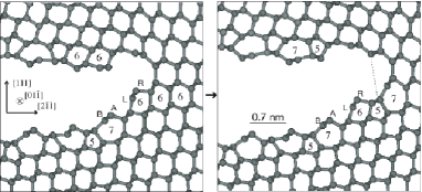
Figure 1 shows an example of the cleavage dynamics with a 10-nm-scale sample or atoms.HOSHI2005 The (111)-21 reconstruction appears on the cleaved surface. Several results contain step formations on the (111)-2 1 surface, as shown in Fig. 1. In Fig. 1, several five-, six-, seven-membered rings are marked as ‘5’, ‘6’ and ‘7’, respectively, as a guide for eye. The 21 reconstruction appears, when the two successive six-membered rings are transformed into a set of five- and seven-membered rings. A characteristic six-membered ring appears at the step-edge region.
Surface atoms on the flat region, form tilted zigzag chains of threefold-coordinated atoms, as explained in the first paragraph of the present section. For example, the atom in Fig. 1 is placed on the vacuum-side (upper) region and the atom is placed on the bulk-side (lower) region. The zigzag chain with the reverse tilting is also obtained. It is remarkable that the surface atoms at the step-edge region, marked as ‘’ and ‘R’, also form a zigzag chains of threefold-coordinated atoms, as on the flat region. One can consider, therefore, that the two tilted structures may be stable at the step-edge region, as on the flat region, although the simulation results contain only one tilted structure in which the atoms is placed on the vacuum-side region and the atoms is on the bulk-side region. Moreover, the calculated LDOS indicates a bias-dependent image of the scanning tunnelling spectroscopy (STM) both on the flat region and the step-edge regions. The peaks in the LDOS profile are located at almost the same positions in the step-edge atoms, such as the and atoms, and the atoms on the flat region, such as the and atoms. A bias-dependent STM image was observed experimentally for the flat region. FEENSTRA86 The calculation predicts the same bias-dependent image on the step-edge region. The same step-edge structures and its bias-dependent STM image were suggested also for Ge cases, because of the similarity of electronic structure. HOSHI2005
3 Ab initio calculations
The properties of the stepped Si(111)-21 surface, predicted by the large-scale calculation, were confirmed by the DFT-PW calculation with a smaller sample. The Vienna ab initio simulation package (VASP) was used with the projector augmented wave method and the local density approximation. VASP
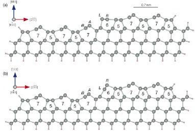
Figure 2 shows the calculated sample that contains 96 silicon atoms in the simulation cell. The sample corresponds to a ‘close up’ of the step-edge region of the large-scale calculation. The sample is periodic only in the direction. and the sample boundary is terminated by artificial hydrogen atoms.
Structures are optimized with several initial guesses and the two tilted step-edge structures in Fig. 2 are obtained as stable ones. The site names of , , and in Fig. 2 are consistent to those in Fig. 1. Hereafter, the structure in Fig. 2 (a) is called ‘L-type’ step-edge structure, since the atom, the left atom of the step edge region, is located at the vacuum-side region and the atom, the right atoms, is located at the bulk-side region. The structure in Fig. 2 (b) indicates the reverse tilting at the step-edge region and is called ‘R-type’ structure. The energy of the -type structure is lower than that of the -type structure by eV per atom pair of the zigzag chain.
Additional calculations were carried out, so as to clarify physical discussions for the two step-edge structures. First, the structures were calculated with different tilting structures on the flat region, in which the zigzag chains on the flat region, such as the and atoms in Fig. 2, form the reverse tilting structure. The calculation result indicates that the above energy difference ( eV) is independent on the tilting strctures of the flat region and that the above energy difference stems from the local tilting structure of the step-edge region. Second, the energy difference was calculated also by the tight-binding form Hamiltonian used in the large-scale calculation and gives eV, which agrees satisfactorily with the above ab initio calculation.
Although the existence of the two stable structures at the step-edge regions is reasonable, as discussed in the previous section, it is interesting that the cleavage simulation of Fig. 1 contains the ‘R-type’ structure, the higher energy structure of the two. The appearance of the higher energy structure in the cleavage simulation can be understood, since the atom is located on an upper position than the atom, in an ideal diamond structure. The simulation realizes the dynamics with the time scale in 10 ps and it might be difficult to reproduce the transformation process from the ‘R-type’ structure into the ‘L-type’ one.
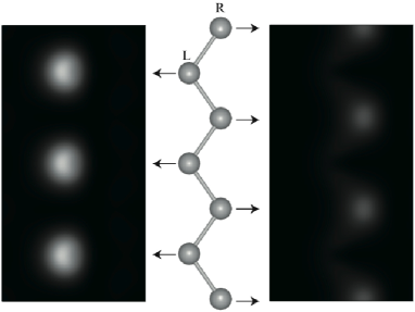
In Fig. 3, the STM images are calculated for the step-edge region of the ‘L-type’ structure. The calculation details are written in the caption. An occupied surface state is localized on the vacuum-side atom (the atom) and an unoccupied surface state is localized on the bulk-side atom (the atom). The calculated STM images for the flat region shows the same bias-dependency. These results are consistent to those of the large-scale calculation. Here it is noteworthy that the STM image for the ‘R-type’ structure should be discussed more carefully, both in theory and experiment, since the height of the and atoms are different significantly, by approximately 1 Å. When STM images were calculated as the constant height calculations, like those for the ‘L-type’ structure in Fig. 3, and the probed height was set to be slightly higher than the atom, the calculated images contain only the images for the atom, like the right panel of Fig. 3, both for the positive and negative bias values, since the atom is placed near the probed height.
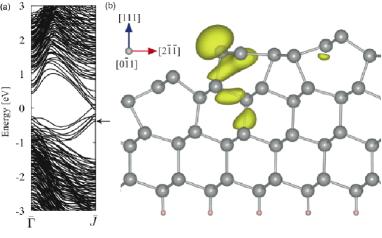
Figure 4 shows (a) the band structure and (b) a characteristic localized wavefunction for the ‘L-type’ step-edge structure. These results are quite similar to those of the flat Si(111)-2x1 surface, since the zigzag chain of threefold-coordinated atoms appears commonly in the two cases. The band structure of the flat Si(111)-2x1 surface is found, for example, in Ref. ROHLFING1999 , in which they use the GW approximation, an advanced electronic structure theory beyond DFT. The surface states are separated from the bulk bands at the point, as a common property among the band structures of the flat surface (Fig. 1 of Ref. ROHLFING1999 ) and the stepped surface (Fig. 4(a)). Figure 4(b) shows a characteristic wavefunction localized at the step-edge region. The corresponding eigen level is placed at the lowest surface state level the point. The level is indicated by the arrow in Fig. 4(a). The wavefunction is a -like state located on the vacuum-side () atom at the step edge region and the same property is seen on the wavefunction on the flat surface (Fig.2(a) of Ref. ROHLFING1999 ). The energy gap between the occupied and unoccupied levels vanishes at the point in Fig. 4(a). It is speculated that the gap is underestimated artificially, as usually within DFT calculations, and a finite gap should appear in a real system, as that of Ref. ROHLFING1999
The same investigation was carried out also for the stepped Ge(111)-2x1 surfaces. The energy of the -type step-edge structure is lower than that of the -type structure, as in the Si case. The energy difference between them is comparable to that in the Si case ( eV). Therefore, the appearance of the stepped (111)-2x1 structure should be understood as a common property of the Si and Ge cases, which is consistent to the discussion in the previous section.
4 Summary
A hierarchical research is presented for the stepped Si and Ge (111)-21 surface in the stable cleavage mode. The present DFT-PW calculation validates the predictions in our previous calculation with the large-scale order- theory HOSHI2005 for (i) the stepped surface structure and (ii) its bias-dependent STM image.
The hierarchical research as a combined study of large-scale calculations with large (10-nm-scale) systems and finer calculations with smaller systems is general and is applicable to various nanomaterials, since all the theories are founded within a general framework of quantum mechanics for electron.
References
- (1) R. Car and M. Parrinello, Phys. Rev. Lett. 55 (1985) 2471
-
(2)
T. Hoshi and T. Fujiwara,
J. Phys. Soc. Jpn. 69 (2000) 3773;
preprint: http://arxiv.org/abs/cond-mat/9910424 - (3) T. Hoshi and T. Fujiwara, Surf. Sci. 493 (2001) 659
-
(4)
T. Hoshi and T. Fujiwara,
J. Phys. Soc. Jpn. 72 (2003) 2429;
preprint: http://arxiv.org/abs/cond-mat/0210366 -
(5)
M. Geshi, T. Hoshi and T. Fujiwara,
J. Phys. Soc. Jpn. 72 (2003) 2880;
preprint: http://arxiv.org/abs/cond-mat/0306461 -
(6)
R. Takayama, T. Hoshi and T. Fujiwara
J. Phys. Soc. Jpn. 73 (2004) 1519
preprint: http://arxiv.org/abs/cond-mat/0401498 -
(7)
T. Hoshi, Y. Iguchi and T. Fujiwara,
Phys. Rev. B 72 (2005) 075323
preprint: http://arxiv.org/abs/cond-mat/0409142 -
(8)
R. Takayama, T. Hoshi, T. Sogabe, S.-L. Zhang and T. Fujiwara ,
Phys. Rev. B73 (2006) 165108
preprint : http://arxiv.org/abs/cond-mat/0503394 -
(9)
T. Hoshi, R. Takayama, Y Iguchi and T. Fujiwara:
Physica B 376-377 (2006) 975
preprint : http://arxiv.org/abs/cond-mat/0508277 -
(10)
T. Hoshi and T. Fujiwara,
J. Phys: Condens. Matter. 18 (2006) 10787
preprint : http://arxiv.org/abs/cond-mat/0610563 -
(11)
T. Hoshi ,
J. Phys: Condens. Matter. 19 (2007) 365243
preprint: http://arxiv.org/abs/0708.0127 -
(12)
Y. Iguchi, T. Hoshi and T. Fujiwara,
Phys. Rev. Lett. 99 (2007) 125507
preprint: http://arxiv.org/abs/cond-mat/0611738 -
(13)
H. Shinaoka, T. Hoshi and T. Fujiwara,
J. Phys. Soc. Jpn. 77 (2008) 114712
preprint: http://arxiv.org/abs/0809.3078 -
(14)
S. Yamamoto, T. Hoshi, T Sogabe, S.-L. Zhang, and T. Fujiwara
J. Phys. Soc. Jpn. 77 (2008) 114713
preprint: http://arxiv.org/abs/0802.2790 -
(15)
T. Hoshi and T. Fujiwara,
J. Phys.: Condens. Matter. 21 (2009) 064233
preprint : http://arxiv.org/abs/0808.1353 -
(16)
T. Hoshi and T. Fujiwara,
J. Phys.: Condens. Matter. 21 (2009) 272201
preprint: http://arxiv.org/abs/0903.1819 - (17) T. Hoshi, Y. Iguchi and T. Fujiwara, to appear in Handbook of Nanophysics, Ed. K. Sattler, Taylor& Francis Publisher.
-
(18)
T. Hoshi, T. Iitaka and M. Fyta,
to appear in J. Phys.: CS.
preprint: http://arxiv.org/abs/0908.4469 - (19) Y. Kondo and K. Takayanagi, Science 289 (2000) 606
- (20) T. Irifune, A. Kurio, A. Sakamoto, T. Inoue and H. Sumiya, Nature 421 (2003) 599; 421 806
- (21) K. C. Pandey, Phys. Rev. Lett. 47 (1981) 1913
- (22) R. M. Feenstra, W. A. Thompson and A. P. Fein Phys. Rev. Lett. 56 (1986) 608; J. A. Stroscio, R. M. Feenstra and A. P. Fein Phys. Rev. Lett. 57 (1986) 2579
- (23) R. M. Feenstra and J. A. Stroscio, Phys. Rev. Lett. 59 (1987) 2173
- (24) F. Ancilotto, W. Andreoni, A. Selloni, R. Car, and M. Parrinello, Phys. Rev. Lett. 65 (1990) 3148
- (25) Y. M. Huang, J. C. H. Spence, O. F. Sankey, and G. B. Adams, Surf. Sci. 256 (1991) 344; J. C. H. Spence, Y. M. Huang, and O. Sankey, Acta Metall. Mater. 41 (1993) 2815
- (26) M. Rohlfing and S. G. Louie: Phys. Rev. Lett.83 (1999) 856.
- (27) R. Pérez and P. Gumbsch, Phys. Rev. Lett. 84 (2000) 5347
- (28) E. Inami and K. Tanimura: Phys. Rev. B76 (2007) 035311
- (29) J. R. Kermode, T. Albaret, D. Sherman, N. Bernstein, P. Gumbsch, M. C. Payne, G. Csányi and A. De Vita, Nature 455, (2008) 1224
- (30) G. Kresse, J. Hafner, Phys. Rev. B, 47 (1993) 558; G. Kresse, J. Furthmüller, Phys. Rev. B, 54 (1996) 11169