Influence of O and N on the conductivity of carbon nanotube networks
Abstract
We have performed experiments on single-wall carbon nanotube (SWNT) networks and compared with density-functional theory (DFT) calculations to identify the microscopic origin of the observed sensitivity of the network conductivity to physisorbed O and N. Previous DFT calculations of the transmission function for isolated pristine SWNTs have found physisorbed molecules have little influence on their conductivity. However, by calculating the four-terminal transmission function of crossed SWNT junctions, we show that physisorbed O and N do affect the junction’s conductance. This may be understood as an increase in tunneling probability due to hopping via molecular orbitals. We find the effect is substantially larger for O than for N, and for semiconducting rather than metallic SWNTs junctions, in agreement with experiment.
pacs:
73.63.–b, 68.43.–h, 73.50.LwI Introduction
Using single-wall carbon nanotubes (SWNTs) as nanosensors, both individually and in SWNT networks, has been one of the most promising potential applications of SWNTs since their discovery. CNTs ; CNT_Sensors_Rev Several experimental studies have demonstrated that the conductance of SWNT systems is rather sensitive to the presence of even single-molecule concentrations of physisorbed gas molecules such as O and N. Ref01 ; Ref03 ; Ref10 ; O2_Plasma ; SWNT_Networks_O2 ; ChrisO2 ; ChrisN2 Further, by measuring conductivity of individually characterized SWNTs, CNT+NH3+NO2 as well as thick (metal-like) and thin (semiconductor-like) SWNT networks, LRef3 ; ChrisO2 ; ChrisN2 the response of SWNTs to contaminants has been shown to correlate with the intrinsic electronic properties of the material. For example, it has been found that the presence of low-O concentrations, independent of temperature, introduces an increase in conductance of approximately 20% on thin SWNT networks, while an increase in conductance of only about 1% is found for thick SWNT networks. ChrisO2
On the other hand, previous theoretical studies have found that SWNTs are rather inert, so that gases tend only to physisorb to the SWNT surface. O_Adsorption_Graphite_NTs ; O2_Adsorption_SWCNTs ; O_Chemisorption_CNTs ; CNT+O2_10_0 ; CNT+O2_physi1 ; CNT+O2_physi2 ; CNT+O2_Triplet ; CNT+O2_8_0 For this reason, it was suggested that O should not effect conductance through SWNTs, but only influence conductance at either SWNT-SWNT junctions, at the SWNT-metal contacts, or at SWNT defect sites. O_Adsorption_Graphite_NTs ; Sensors Although the conductivity of SWNTs with molecules physisorbed at defect sites has been extensively studied, CNT_Doped_Theory ; O2_Defects ; CNT_Defects_Conductance the conductivity of four-terminal SWNT-SWNT junctions has been previously studied only for small pristine metallic SWNTs. ExpCrossedCNTs ; Junction_Conductance The possible influence of physisorbed molecules on SWNT-SWNT junctions has not been investigated.
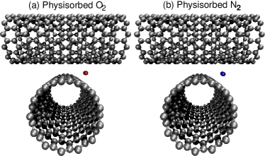
In this paper we address the microscopic origin of the increase in conductance of SWNT networks when exposed to O or N gas. To this end, we have performed density-functional theory (DFT) calculations of the intratube transmission within a SWNT and the intertube transmission between two SWNTs in the nonequilibrium Green’s function (NEGF) formalism for O and N molecules physisorbed in (7,7) metallic armchair, (12,0) semimetallic zigzag, and (13,0) semiconducting zigzag SWNT junctions, shown schematically in Fig. 1. Comparing our theoretical results for SWNT junctions with experimental measurements for SWNT networks suggests that the surprising sensitivity to O and N may be partially due to an increased tunneling probability through O and N physisorbed at SWNT junctions.
In Sec. II we describe experimental measurements of the influence of both O and N on the conductivity of SWNT networks and the characterization of these networks using Raman spectroscopy. A description of the DFT and NEGF model used to describe the microscopic origin of this effect is then provided in Sec. III. In Sec. IV we compare our theoretical results for the SWNT junction transmission with the SWNT network experiments, followed by a concluding section.
II Experimental Results
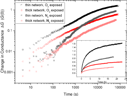
Below we give a brief discussion of our experiments on SWNT network conductivity. A more detailed description may be found in Refs. ChrisO2, and ChrisN2, . Figure 2 shows experimental measurements of the conductance sensitivity to O and N exposure for thick and thin SWNT networks. These samples were initially placed under vacuum ( mbar) and irradiated by a UV light-emitting diode (LED) ( 400 nm) at low intensity (0.03 mW/cm) for approximately 12 h to desorb surface and interbundle adsorbates (surface dopants) from the SWNTs. Once the SWNT network’s conductance stabilized, the samples were exposed to either O (99.5% pure) or N (99.998% pure) at 1 atm. The conductance of the samples was then monitored by periodically sampling ( 1 s) the current while applying a fixed bias of 1 mV to the thick (metal-like) SWNT network ( 1 k) and 10 mV to the thin (semiconductor-like) SWNT network ( 1000 k), as shown in Fig. 2.
After 5 min of exposure to O, the thin network shows an increase in conductance of about 13% while the thick network’s conductance changes by about 7%. For the same exposure to N, both networks show substantially smaller conductance changes of 2%–3%. However, at exposure times of more than 2 h, the thin SWNT network response to N is similar to that of the thick SWNT network to O. This might be caused by a weaker physisorption of N to the SWNT networks than O. The inset of Fig. 2 also shows that at very long exposure times the fractional change in conductance, , becomes saturated after 24 h. Further, the response to O depicted in Fig. 2 shows that the conductance change for a thin SWNT network is about two to three times that of the thick SWNT network at all times. This suggests that the conductance change under O exposure is an intrinsic property of the SWNT networks, present even at very low O concentrations. Herein we shall focus on the microscopic origin of the network sensitivity to O and N, with the temporal behavior of the networks discussed elsewhere. ChrisO2 ; ChrisN2
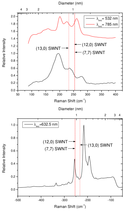
We have performed the Raman spectroscopy to characterize our SWNT network samples, which were produced via the high-pressure carbon monoxide (HiPco) method. Figure 3 shows the radial breating mode (RBM) Raman signals of HiPco samples at excitation wavelengths 532 nm, 632.5 nm and 785 nm. The van Hove singularity energy separation was calculated using the tight-binding approximation with the carbon-carbon interaction energy 2.9 eV and carbon-carbon bond length 1.44 Å. The SWNT diameter dependence of the RBM frequency for isolated SWNTs on SiO has been shown raman_nanotube to behave as . The DFT calculated diameters for (7,7), (12,0), and (13,0) SWNTs of 9.76, 9.79, and 10.66 Å, respectively, are found to correlate well with the HiPco Raman shift, as shown in Fig. 3. This should ensure a good description of the SWNT network’s work function, which may be significantly different for smaller tubes.
III Basic Theory
Our DFT calculations have been performed with the siesta DFT code ASE ; SIESTA using a double-zeta polarized (DZP) basis set for the physisorbed molecules (O and N), and a single-zeta polarized (SZP) basis set for the SWNTs (C), and the Perdew-Burke-Ernzerhof exchange-correlation functional. PBE We note here that the DZP and SZP siesta basis sets have recently been shown to yield transmission functions in quantitative agreement with plane-wave codes and maximally localized Wannier functions. BenchmarkPaper When modeling O we have performed spin-polarized calculations O_Adsorption_Graphite_NTs but have performed spin- unpolarized calculations otherwise.
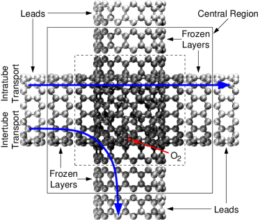
We have modeled the junction system using 6(11) primitive unit cells or layers for each zigzag(armchair) SWNT per supercell, with a separation of approximately 3.4 Å, as depicted for a (13,0) SWNT junction in Figs. 1 and 4. Jesper The four SWNT layers at the boundaries of the central region, shown in gray in Fig. 4, were kept fixed at their relaxed positions in the isolated SWNT. At the same time the central 4(9) primitive unit cells from each tube, shown in dark gray in Fig. 4, and the physisorbed molecules were relaxed until a maximum force of less than 0.1 eV/Å was obtained. Since the supercell has dimensions of Å for each SWNT junction, a point calculation was sufficient to describe the periodicity of the structure.
Such a large supercell was necessary for the Hamiltonian of each of the four SWNT layers adjacent to the boundaries , to be within 0.1 eV of the Hamiltonian for the respective leads , so that 0.1 eV. In this way the electronic structure at the edges of the central region was ensured to be converged to that in the leads.
| (%) | [Å] | |||
|---|---|---|---|---|
| SWNT Junction | O | N | SWNT-O | SWNT-N |
| (7,7) Armchair | 30 | 6 | 2.3 | 2.8 |
| (12,0) Zigzag | 140 | 14 | 2.6 | 2.8 |
| (13,0) Zigzag | 1800 | 130 | 2.5 | 2.8 |
The Landauer-Bütticker conductance for a multi-terminal system can be calculated from the Green’s function of the central region, , according to the formula Meir ; Thygesen2 ; 4TConductance
| (1) |
where the trace runs over all localized basis functions in the central region. To describe the conductance at small bias for semiconducting systems, the Fermi energy should be taken as the energy of the valence-band maximum or conduction-band minimum for -type and -type semiconductors, respectively. The central region Green’s function is calculated from
| (2) |
where , and are the overlap matrix and Kohn-Sham Hamiltonian matrix of the central region in the localized basis, is the self-energy of lead ,
| (3) |
and the coupling elements between the central region and lead for the overlap and Kohn-Sham Hamiltonian are and respectively.
The coupling strengths of the input and output leads are then given by . For a four-terminal SWNT junction, the intratube and intertube transmission functions are calculated by choosing the appropriate output lead, as depicted in Fig. 4.
IV Theoretical Results & Discussion
For each of the three types of SWNT junctions considered, we find that both O and N are physisorbed with binding energies of 0.2 eV, as depicted in Fig. 1. Further, the SWNT–O and SWNT–N equilibrium separation distance is in the range 2.3—2.8 Å, as given in Table 1. These results agree qualitatively with previous theoretical studies for O binding distances and energies on isolated SWNTs. O_Adsorption_Graphite_NTs ; O2_Adsorption_SWCNTs ; O_Chemisorption_CNTs ; CNT+O2_10_0 ; CNT+O2_physi1 ; CNT+O2_physi2 ; CNT+O2_Triplet ; CNT+O2_8_0
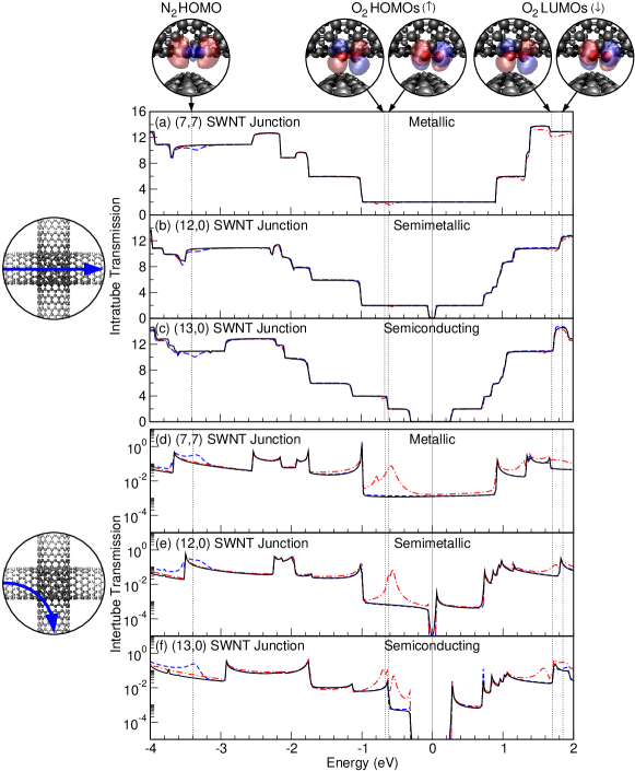
Figures 5(a)-5(c) show the intratube transmission for three prototypical SWNTs commonly found in experimental HiPco samples, Photoluminescence as shown in Fig. 3. In Fig. 5(a) we see that for a metallic armchair (7,7) SWNT, transmission occurs through two channels at the Fermi level. We see in Fig. 5(b) that the conductance for the semimetallic zigzag (12,0) SWNT resembles that found in Fig. 5(a) for a metallic SWNT, except for a tiny band gap of 0.05 eV at the Fermi level. In Fig. 5(c) we find for a semiconducting zigzag (13,0) SWNT a band gap of approximately 0.6 eV between the valence and conduction bands, through which no transmission occurs. This is only slightly smaller than the expected band gap of 0.7 eV, based on a fit to experimental data.ExpDOS_10_0 These results for the intratube transmission of pristine SWNTs also agree qualitatively with previous DFT studies of isolated (5,5), (10,10), (10,5), (11,0), and (12,0) SWNTs. DOS_1010_105 ; Junction_Conductance ; Rev_CNTTransport We also find in Figs. 5(a)–5(c) that neither O nor N physisorbed at a SWNT junction noticeably influence the intratube transmission.
In Fig. 5 we also show isosurfaces and eigenenergies for the highest occupied and lowest occupied molecular orbitals (HOMO and LUMO) on physisorbed O and N. For these weakly coupled molecules, the renormalized molecular levels may easily be identified with the molecular orbitals of the free O and N molecules. Thygesen1 Since the position of the molecular levels is rather insensitive to the type of junction, it should also be insensitive to the exact binding geometry. This suggests that additional physisorbed molecules will influence the intertube transmission similarly.
We find the intertube transmission is proportional to the density of states (DOS) for the system with peaks in the transmission at the van Hove singularities. This is consistent with transport between the SWNTs occurring in the tunneling regime, as expected for a SWNT separation of approximately 3.4 Å.
The presence of physisorbed molecules in the SWNT-SWNT gap should then increase the tunneling probability at energies near the eigenenergies of the molecular orbitals. This is evidenced by the distinct peaks in the intertube transmission for each SWNT junction at energies corresponding to the HOMO of N and the spin polarized HOMOs and LUMOs of O, as seen in Figs. 5(d)–5(f). Under such conditions, a SWNT junction behaves as a simple tunneling electron microscopy (TEM) tip. By applying appropriate bias voltages, one may potentially probe the molecular orbitals of a physisorbed molecule to determine its chemical composition.
For this reason, the sensitivity of SWNT network conductivity to O is at least partly due to the close proximity of the O HOMOs to the Fermi energies of typical SWNTs ( 0.6 eV), as shown in Fig. 5. Further, it has been shown experimentally that defects inherent in physically realizable SWNTs yield -type semiconductors.CNTs ; p-type ; p-type_n-type The conductivity measured experimentally at small bias is thus at the energy of the valence band .
As seen in Fig. 5(f), the O HOMO eigenenergy is only about 0.3 eV below for a semiconducting (13,0) SWNT junction. As shown in Table 1, this yields a substantial increase in the intertube conductance at zero bias for semiconducting junctions in the presence of O, while much smaller increases are found for the metallic and semimetallic junctions, in agreement with experiment. ChrisO2 On the other hand, we also find physisorbed N increases the intertube conductance only slightly, also in qualitative agreement with experiment, Ref10 as shown in Fig. 2.
Although it is well-known DFT calculations underestimate band gaps, DOS_1010_105 ; UnderestimateBG2 ; UnderestimateBG1 since we are primarily interested in how the presence of O or N qualitatively changes the DOS and conductance, such calculations are still useful.
V Conclusions
In conclusion, we have proposed a possible microscopic explanation for the experimentally observed sensitivity of the electrical conductance of carbon nanotube networks to oxygen and nitrogen gases. Our DFT calculations suggests that O and N physisorbed in crossed SWNT junctions can have a large influence on the intertube conductance. In particular, for O the close proximity of the highest occupied molecular orbitals with the Fermi level of the SWNT significantly increases electron tunneling across the gap. The effect is found to be larger for O than for N and for semiconducting rather than metallic SWNTs, in agreement with the experimental observations. Our results suggests that the electrical properties of SWNT networks are to a large extent determined by crossed SWNT junctions.
Acknowledgements.
We thank E. I. Kauppinen, and K. W. Jacobson for useful discussions. D.J.M. and K.S.T. acknowledge financial support from NABIIT and the Danish Center for Scientific Computing under Grant No. HDW-1103-06. The Center for Atomic-scale Materials Design (CAMD) is sponsored by the Lundbeck Foundation. C. M. acknowledges financial support from the National Physical Laboratory (NPL) and the Engineering and Physical Sciences Research Council (EPSRC-GB).References
- (1) M. S. Dresselhaus, G. Dresselhaus, and P. Avouris, eds., Carbon Nanotubes: Sythesis, Structure, Properties, and Applications (Springer, Berlin, 2001).
- (2) D. R. Kauffman and A. Star, “Carbon nanotube gas and vapor sensors”, Angew. Chem. 47(35), 6550 (Jul. 2008), doi:10.1002/anie.200704488.
- (3) K. Bradley, S.-H. Jhi, P. G. Collins, J. Hone, M. L. Cohen, S. G. Louie, and A. Zettl, “Is the intrinsic thermoelectric power of carbon nanotubes positive?”, Phys. Rev. Lett. 85(20), 4361 (Nov. 2000), doi:10.1103/PhysRevLett.85.4361.
- (4) P. G. Collins, K. Bradley, M. Ishigami, and A. Zettl, “Extreme oxygen sensitivity of electronic properties of carbon nanotubes”, Science 287(5459), 1801 (Mar. 2000), doi:10.1126/science.287.5459.1801.
- (5) G. U. Sumanasekera, C. K. W. Adu, S. Fang, and P. C. Eklund, “Effects of gas adsorption and collisions on electrical transport in single-walled carbon nanotubes”, Phys. Rev. Lett. 85(5), 1096 (Jul. 2000), doi:10.1103/PhysRevLett.85.1096.
- (6) A. Felten, J. Ghijsen, J.-J. Pireaux, R. L. Johnson, C. M. Whelan, D. Liang, G. V. Tendeloo, and C. Bittencourt, “Effect of oxygen rf-plasma on electronic properties of CNTs”, J. Phys. D 40(23), 7379 (Dec. 2007), doi:10.1088/0022-3727/40/23/019.
- (7) M. Kaempgen, M. Lebert, M. Haluska, N. Nicoloso, and S. Roth, “Sonochemical optimization of the conductivity of single-wall carbon nanotube networks”, Adv. Mater. 20(3), 616 (Jan. 2008), doi:10.1002/adma.200702873.
- (8) C. Morgan, Z. Alemipour, and M. Baxendale, “Variable range hopping in oxygen-exposed single-wall carbon nanotube networks”, Phys. Stat. Solidi A 205(6), 1394 (2008), doi:10.1002/pssa.200778113.
- (9) C. Morgan and M. Baxendale, “Diffusion of O and N through thin and thick SWNT networks” (May 2009), arXiv:0905.1821v1.
- (10) J. Kong, N. R. Franklin, C. Zhou, M. G. Chapline, S. Peng, K. Cho, and H. Dai, “Nanotube molecular wires as chemical sensors”, Science 287(5453), 622 (Jan. 2000), doi:10.1126/science.287.5453.622.
- (11) V. Skákalová, A. B. Kaiser, Y.-S. Woo, and S. Roth, “Electronic transport in carbon nanotubes: From individual nanotubes to thin and thick networks”, Phys. Rev. B 74(8), 085403 (Aug. 2006), doi:10.1103/PhysRevB.74.085403.
- (12) P. Giannozzi, R. Car, and G. Scoles, “Oxygen adsorption on graphite and nanotubes”, J. Chem. Phys. 118(3), 1003 (Jan. 2003), doi:10.1063/1.1536636.
- (13) A. Tchernatinsky, S. Desai, G. U. Sumanasekera, C. S. Jayanthi, S. Y. Wu, B. Nagabhirava, and B. Alphenaar, “Adsorption of oxygen molecules on individual single-wall carbon nanotubes”, J. Appl. Phys. 99, 034306 (Feb. 2006), doi:10.1063/1.2163008.
- (14) V. A. Margulis and E. E. Muryumin, “Atomic oxygen chemisorption on the sidewall of zigzag single-walled carbon nanotubes”, Phys. Rev. B 75(3), 035429 (Jan. 2007), doi:10.1103/PhysRevB.75.035429.
- (15) S. Peng and K. Cho, “Chemical control of nanotube electronics”, Nanotechnology 11(2), 57 (Jun. 2000), doi:10.1088/0957-4484/11/2/303.
- (16) D. C. Sorescu, K. D. Jordan, and P. Avouris, “Theoretical study of oxygen adsorption on graphite and the (8,0) single-walled carbon nanotube”, J. Phys. Chem. B 105(45), 11227 (Oct. 2001), doi:10.1021/jp0122979.
- (17) D. J. Mann and W. L. Hase, “Direct dynamics simulations of the oxidation of a single wall carbon nanotube”, Phys. Chem. Chem. Phys. 3(19), 4376 (Aug. 2001), doi:10.1039/b103762p.
- (18) S.-H. Jhi, S. G. Louie, and M. L. Cohen, “Electronic properties of oxidized carbon nanotubes”, Phys. Rev. Lett. 85(8), 1710 (2000), doi:10.1103/PhysRevLett.85.1710.
- (19) S.-P. Chan, G. Chen, X. G. Gong, and Z.-F. Liu, “Oxidation of carbon nanotubes by singlet O”, Phys. Rev. Lett. 90(8), 086403 (Feb. 2003), doi:10.1103/PhysRevLett.90.086403.
- (20) A. R. Rocha, M. Rossi, A. Fazzio, and A. J. R. da Silva, “Designing real nanotube-based gas sensors”, Phys. Rev. Lett. 100(17), 176803 (May 2008), doi:10.1103/PhysRevLett.100.176803.
- (21) S. Peng and K. Cho, “Ab initio study of doped carbon nanotubes sensors”, Nano Lett. 3(4), 513 (Mar. 2003), doi:10.1021/nl034064u.
- (22) P. C. P. Watts, N. Mureau, Z. Tang, Y. Miyajima, J. D. Carey, and S. R. P. Silva, “The importance of oxygen-containing defects on carbon nanotubes for the detection of polar and non-polar vapours through hydrogen bond formation”, Nanotechnology 18(17), 175701 (May 2007), doi:10.1088/0957-4484/18/17/175701.
- (23) P. C. P. Watts, W.-K. Hsu, H. W. Kronto, and D. R. M. Walton, “Are bulk defective carbon nanotubes less electrically conducting?”, Nano Lett. 3(4), 549 (Mar. 2003), doi:10.1021/nl034028v.
- (24) M. S. Fuhrer, J. Nygård, L. Shih, M. Forero, Y.-G. Yoon, M. S. C. Mazzoni, H. J. Choi, J. Ihm, S. G. Louie, A. Zettl, and P. L. McEuen, “Crossed nanotube junctions”, Science 288(5465), 494 (Apr. 2000), doi:10.1126/science.288.5465.494.
- (25) Y.-G. Yoon, M. S. C. Mazzoni, H. J. Choi, J. Ihm, and S. G. Louie, “Structural deformation and intertube conductance of crossed carbon nanotube junctions”, Phys. Rev. Lett. 86(4), 688 (Jan. 2001), doi:10.1103/PhysRevLett.86.688.
- (26) A. Jorio, R. Saito, J. H. Hafner, C. M. Lieber, M. Hunter, T. McClure, G. Dresselhaus, and M. S. Dresselhaus, “Structural (n, m) determination of isolated single-wall carbon nanotubes by resonant raman scattering”, Phys. Rev. Lett. 86(6), 1118 (Feb. 2001), doi:10.1103/PhysRevLett.86.1118.
- (27) S. R. Bahn and K. W. Jacobsen, “An object-oriented scripting interface to a legacy electronic structure code”, Comput. Sci. Eng. 4(3), 56 (May 2002), doi:10.1109/5992.998641.
- (28) J. M. Soler, E. Artacho, J. D. Gale, A. Garcia, J. Junquera, P. Ordejón, and D. Sánchez-Portal, “The SIESTA method for ab initio order- materials simulation”, J. Phys.: Condens. Matter 14(11), 2745 (Mar. 2002), doi:10.1088/0953-8984/14/11/302.
- (29) J. P. Perdew, K. Burke, and M. Ernzerhof, “Generalized gradient approximation made simple”, Phys. Rev. Lett. 77(18), 3865 (Oct. 1996), doi:10.1103/PhysRevLett.77.3865.
- (30) M. Strange, I. S. Kristensen, K. S. Thygesen, and K. W. Jacobsen, “Benchmark density functional theory calculations for nanoscale conductance”, J. Chem. Phys. 128(11), 114714 (Mar. 2008), doi:10.1063/1.2839275.
- (31) J. Kleis, P. Hyldgaard, and E. Schröder, “Van der Waals interaction of parallel polymers and nanotubes”, Comput. Mater. Sci. 33(1–3), 192 (Jan. 2005), doi:10.1016/j.commatsci.2004.12.036.
- (32) Y. Meir and N. S. Wingreen, “Landauer formula for the current through an interacting electron region”, Phys. Rev. Lett 68(16), 2512 (Apr. 1992), doi:10.1103/PhysRevLett.68.2512.
- (33) K. S. Thygesen, “Electron transport through an interacting region: The case of a nonorthogonal basis set”, Phys. Rev. B 73(3), 035309 (Jan. 2006), doi:10.1103/PhysRevB.73.035309.
- (34) M. Buttiker, “Four-terminal phase-coherent conductance”, Phys. Rev. Lett. 57(14), 1761 (Oct. 1986), doi:10.1103/PhysRevLett.57.1761.
- (35) Z. Luo, L. D. Pfefferle, G. I. Haller, and F. Papadimitrakopoulos, “(n,m) abundance evaluation of single-walled carbon nanotubes by fluorescence and absorption spectroscopy”, J. Am. Chem. Soc. 128(48), 15511 (Nov. 2006), doi:10.1021/ja0657096.
- (36) T. W. Odom, J.-L. Huang, P. Kim, and C. M. Lieber, “Structure and electronic properties of carbon nanotubes”, J. Phys. Chem. B 104(13), 2794 (Feb. 2000), doi:10.1021/jp993592k.
- (37) S. Reich, C. Thomsen, and P. Ordejón, “Electronic band structure of isolated and bundled carbon nanotubes”, Phys. Rev. B 65(15), 155411 (Apr. 2002), doi:10.1103/PhysRevB.65.155411.
- (38) J.-C. Charlier, X. Blase, and S. Roche, “Electronic and transport properties of nanotubes”, Rev. Mod. Phys. 79(2), 677 (May 2007), doi:10.1103/RevModPhys.79.677.
- (39) K. S. Thygesen and K. W. Jacobsen, “Molecular transport calculations with Wannier functions”, Chem. Phys. 319(1–3), 111 (Dec. 2005), doi:10.1016/j.chemphys.2005.05.032.
- (40) S. J. Tans, A. R. M. Vershueren, and C. Dekker, “Room-temperature transistor based on a single carbon nanotube”, Nature 393, 49 (May 1998), doi:10.1038/29954.
- (41) V. Derycke, R. Martel, J. Appenzeller, and P. Avouris, “Carbon nanotube inter- and intramolecular logic gates”, Nano Lett. 1(9), 453 (Sep. 2001), doi:10.1021/nl015606f.
- (42) J. Paier, M. Marsman, K. Hummer, G. Kresse, I. C. Gerber, and J. G. Ángyán, “Screened hybrid density functionals applied to solids”, J. Chem. Phys. 124(15), 154709 (Apr. 2006), doi:10.1063/1.2187006.
- (43) J. Heyd, J. E. Peralta, G. E. Scuseria, and R. L. Martin, “Energy band gaps and lattice parameters evaluated with the Heyd-Scuseria-Ernzerhof screened hybrid functional”, J. Chem. Phys. 123(17), 174101 (Oct. 2005), doi:10.1063/1.2085170.