Multiband effective bond-orbital model for nitride semiconductors with wurtzite structure
Abstract
A multiband empirical tight-binding model for group-III-nitride semiconductors with a wurtzite structure has been developed and applied to both bulk systems and embedded quantum dots. As a minimal basis set we assume one -orbital and three -orbitals, localized in the unit cell of the hexagonal Bravais lattice, from which one conduction band and three valence bands are formed. Non-vanishing matrix elements up to second nearest neighbors are taken into account. These matrix elements are determined so that the resulting tight-binding band structure reproduces the known -point parameters, which are also used in recent -treatments. Furthermore, the tight-binding band structure can also be fitted to the band energies at other special symmetry points of the Brillouin zone boundary, known from experiment or from first-principle calculations. In this paper, we describe details of the parametrization and present the resulting tight-binding band structures of bulk GaN, AlN, and InN with a wurtzite structure. As a first application to nanostructures, we present results for the single-particle electronic properties of lens-shaped InN quantum dots embedded in a GaN matrix.
pacs:
78.67.Hc, 73.22.Dj, 71.15.Ap, 73.21.LaI Introduction
Due to their unique physical properties, zero-dimensional semiconductor nanostructures, realized by either epitaxial growth or colloidal chemical synthesis, Guzelian et al. (1996) offer a broad range of applications.Michler (2009) The three-dimensional confinement of spatially localized charge carriers in such tailor-made systems leads to a discrete and tunable one-particle spectrum, which can be used for a variety of optoelectronic applications, for quantum computing and quantum cryptography, and even for nanobiological applications like biological flourescence labeling. Bruchez et al. (1998); Michalet et al. (2005)
Most binary group II-VI and III-V semiconductor materials and their ternary and quaternary alloys crystallize in the cubic zincblende or in the hexagonal wurtzite phase, so the corresponding nanostructures can also be attributed to one of these two structures. Dependent on the material system and the adequate parameter range of the experimental conditions (e.g. growth temperature and substrate type for epitaxial growth, additionally the chemical environment and particle size for colloidal synthesis), it is even possible nowadays to realize either of the two structures for the same compounds. For example, epitaxially grown GaN/AlN quantum dots can be produced in the metastable zincblende modification and in the thermodynamically stable wurtzite configuration. Lazar et al. (2004)
The calculation of the optical properties of such systems requires the knowledge of a set of single particle eigenstates and eigenvalues for the confined carriers (electrons and holes), which can be obtained by means of different methods. Rather simple models like effective mass approximations Grundmann et al. (1995); Wojs et al. (1996); Shi and Gan (2003) can give a first insight into the behaviour of such systems. Multiband -models Fonoberov and Balandin (2003); Pryor (1998); Stier et al. (1999); Andreev and O’Reilly (2000) incorporate higher effects like valence band mixing, but still make use of the envelope function approximation, thus not resolving the characteristic underlying lattice structure. Nevertheless, they have been succesfully applied to various material systems and were extended by the inclusion of strain and piezoelectricity effects.
Empirical pseudopotential models (EPM) Wang and Zunger (1996, 1999); Wang et al. (2000); Bester and Zunger (2005) and empirical tight-binding models (ETBM) Santoprete et al. (2003); Schulz and Czycholl (2005, 2006); Schulz et al. (2006, 2008); Korkusinski et al. (2008) allow for the possibility of a microscopic description of nanostructures. While the EPM is capable of resolving variations on the atomic scale, it requires a large set of basis states, which limits the application of these models to small nanostructures. The ETBM uses a coarse graining on the scale of lattice sites, which makes it possible to stick to a small set of basis states and perform calculations on larger supercells with feasible effort. Additionally, it gives a rather intuitive real-space picture of the system in terms of localized Wannier states. The coupling between different lattice sites is usually limited to first or second nearest neighbors, depending on the purpose. The goal is to analytically deduce a manageable set of equations for the tight-binding (TB) matrix elements in terms of bulk parameters (e.g. the band gap, effective masses, spin-orbit splitting) which can be accessed either from experiment or from first-principle calculations like DFT - LDA or recent -results. Rinke et al. (2006, 2008) These TB matrix elements then enter the nanostructure calculation.
When establishing an empirical tight-binding model, one can start from a Löwdin-orthogonalized atomic basis and use a linear combination of atomic orbitals (LCAO) as ansatz for the required eigenstates. Slater and Koster (1954) For nitride semiconductors with a wurtzite structure this has been done recently by Schulz et al. Schulz et al. (2006) But it is as well justified to start from “effective bond-orbitals”, i.e. Wannier-like orbitals localized within a unit cell. Within the LCAO spirit, these effective orbitals can in principle be expressed as linear combinations of the above mentioned atomic orbitals. Neither the atomic orbitals nor the effective orbitals are explicitly known or required within an empirical TB approach, as only the matrix elements between those orbitals are needed to obtain the TB band structure. Therefore, it is equally justified to perform the parametrization directly for the effective bond-orbitals so that known bulk band structure properties are reproduced. Such a version of an ETBM is commonly called “effective bond-orbital model“ (EBOM). The EBOM has the advantage that it usually allows for a better fit throughout the whole Brillouin zone (BZ) within a given basis set.
The EBOM has long been established for the cubic zincblende structure; a first EBOM parametrization by Chang Chang (1988) incorporated three-center overlap integrals in a basis set of one - and three -orbitals on each site of the fcc Bravais lattice. This parametrization was restricted to coupling up to nearest neighbors, so that only the band energies at the -point were fitted, besides the usual set of effective conduction band masses and corresponding valence band parameters. Loehr augmented this model in Ref. Loehr, 1994 by the inclusion of hopping up to second-nearest neighbors to additionaly fit the band-structure of the bulk material to an extended parameter set, including the -point energies. This resulted in a better agreement of the resulting tight-binding conduction band with first-principle calculations. Fritsch et al. (2004)
To our knowledge, there exists only one parametrization of the EBOM for materials with wurtzite structure in the literature. Chen (2004) As this work is restricted to a nearest neighbor parametrization and a fit to zone center energies only, we developed a new parametrization including second nearest neighbor matrix elements and a fit to band energies at other special BZ points. We apply this EBOM to the calculation of the electronic properties of lens-shaped InN quantum dots embedded within GaN.
This work is organized as follows. In Sec. II, our specific EBOM is presented. We developed a second nearest neighbor parametrization. Furthermore, we describe the application to zero-dimensional nanostructures and discuss the inclusion of strain and piezoelectric fields. In Sec. III, the one-particle spectrum for a lens-shaped InN quantum dot embedded within GaN and a comparison with results from other - and fully microscopic ETBM calculations is given. Section IV contains a summary, a conclusion and a brief outlook to possible extensions of our model.
II Theory
II.1 Effective bond-orbital model for bulk semiconductors
Linear combinations of atomic orbitals within one unit cell can be used as ansatz for the Wannier functions localized within the unit cell of the Bravais lattice. From these Wannier functions, the extended Bloch functions can be determined by means of a unitary transformation. As neither the atomic states nor the Wannier functions are explicitly used in an empirical tight-binding model, it is not necessary to start from the atomic wave functions, but one can directly assume a basis of Wannier-like functions, which is the basic idea of the EBOM approach.
As the conduction band wave functions at the BZ center predominantly transform -like with some character, while the corresponding valence band wave functions transform like -states with some character, we use a localized basis per spin direction:
| (1) |
Here labels the sites of the hexagonal lattice, which is the underlying Bravais lattice of the wurtzite crystal structure.
A trial wave function that satisfies the Bloch condition is the Bloch sum
| (2) |
The band structure is now given by the solution of the secular equation
| (3) |
for each wave vector , where
| (4) |
The EBOM matrix elements of the bulk Hamiltonian are thus given by
| (5) |
It should explicitly be pointed out that the artificial change of point group symmetry from (wurtzite) to (hexagonal lattice) in the EBOM approach does not uniquely stem from the omission of the atomic basis, but rather from the specific set of basis functions used. For instance, the original inversion asymmetry of the wurtzite crystal could be restored when the set of basis functions, Eq. (1), is extended by states that are not parity eigenstates. This has been done for cubic systems by Cartoixà et al. in Ref. Cartoixá et al., 2003.
To include the influence of spin-orbit coupling, we follow Ref. Chadi, 1977. As we expect the spin-orbit part of to be of weak influence, we assume only site-diagonal contributions, which stem from the -orbitals. Additionally, the non-ideal lattice constant ratio energetically seperates the - from the - and the -orbitals. These effects can properly be incorporated by introduction of one spin-orbit splitting parameter and one crystal field splitting parameter .
When restricting the non-vanishing matrix elements, Eq. (5), up to nearest or second nearest neighbors, the secular equation (3) can be solved analytically for high symmetry points throughout the BZ of the hexagonal lattice. This yields a set of equations for the EBOM matrix elements in terms of the energetic positions of the bands at the critical -values. By expanding the elements of Eq. (4) around the BZ center and comparing the matrix representation to a corresponding -Hamiltonian, Winkelnkemper et al. (2006); Chuang and Chang (1996) it is possible to deduce additional constraints in terms of the conduction band effective masses and corresponding valence band parameters.
The goal is to arrive at a solvable set of equations which link a sufficiently large number of to a desired set of band structure parameters. In practice, this will require the additional omission of either matrix elements or band parameters, as the system of equations becomes rather complicated. The low symmetry of the hexagonal lattice will result in a larger number of independent parameters and equations than in the case of cubic crystal systems. An overview of the results for a coupling up to second nearest neighbors is given in Tab. 1. More details on the parametrization are given in App. A.
| Second nearest neighbor coupling: | 26 EBOM matrix elements |
|---|---|
| Band parameter | Description |
| direct band gap at | |
| , | effective electron masses |
| , , , , , | valence band parameters |
| spin-orbit splitting | |
| crystal field splitting | |
| , , | -point energies |
| , , , | -point energies |
| , , , | -point energies |
| , , | -point energies |
| Kane parameters |
The band structure for this parametrization is now obtained by the diagonalization of the matrix , Eq. (4), for each .
For all calculations in the present paper, two distinct parameter sets have been used. The first parameter set is derived from a consistent set of band parameters Rinke et al. (2008) obtained from calculations based on exact-exchange optimized effective potential ground states (OEPx), Rinke et al. (2005) supplemented by additional band structure energies at high symmetry points. Rinke (2009) Since the @OEPx band gaps and crystal field splittings still differ slightly from the experimental values, we decided to use a second parameter set, in which these values were replaced by the parameters recommended by Vurgaftman and Meyer in 2003. Vurgaftman and Meyer (2003) To obtain the correct band gaps, all conduction band energies from the calculations were shifted by the respective difference in the second parameter set. Moreover, we used the spin-orbit splittings of Ref. Vurgaftman and Meyer, 2003 in both sets, as the calculations did not include the electron spin. This should be a reasonable approach, as the spin-orbit splitting is comparatively small in these systems. The two parameter sets are listed in Tab. 2 and will be referred to simply as ” parameters“ and ”corrected parameters” from now on.
In our opinion, the corrected parameters should clearly be preferred, as it is known that even highly sophisticated ab-initio approaches still do not properly reproduce the band gap.
| Reference | parameters | Corrected parameters | ||||
|---|---|---|---|---|---|---|
| Material: | AlN | GaN | InN | AlN | GaN | InN |
| [Å] | 3.110 | 3.190 | 3.540 | |||
| [Å] | 4.980 | 5.189 | 5.706 | |||
| [eV] | 6.464 | 3.239 | 0.694 | 6.250 | 3.510 | 0.78 |
| [eV] | 0.019 | 0.017 | 0.005 | |||
| [eV] | -0.295 | 0.034 | 0.066 | -0.169 | 0.010 | 0.040 |
| [eV] | 16.972111For a given band gap, are not independent parameters when are known (see Eqs. (8) - (10)) in App. A. To obtain a better fit to the - band structure, these parameters can be adjusted by least-square fit values, see Ref. Rinke et al., 2008. When the band gap is subsequently altered, as in the set to the right, the analytic expression has to be used again. | 17.29211footnotemark: 1 | 8.74211footnotemark: 1 | |||
| [eV] | 18.16511footnotemark: 1 | 16.26511footnotemark: 1 | 8.80911footnotemark: 1 | |||
| [] | 0.32211footnotemark: 1 | 0.18611footnotemark: 1 | 0.06511footnotemark: 1 | |||
| [] | 0.32911footnotemark: 1 | 0.20911footnotemark: 1 | 0.06811footnotemark: 1 | |||
| -3.991 | -5.947 | -15.803 | ||||
| -0.311 | -0.528 | -0.497 | ||||
| 3.671 | 5.414 | 15.251 | ||||
| -1.147 | -2.512 | -7.151 | ||||
| -1.329 | -2.510 | -7.060 | ||||
| -1.952 | -3.202 | -10.078 | ||||
| [eV] | 8.844 | 5.701 | 3.355 | 8.631 | 5.972 | 3.441 |
| [eV] | -0.686 | -0.597 | -0.509 | |||
| [eV] | -3.573 | -4.110 | -3.581 | |||
| [eV] | 7.545 | 5.798 | 4.356 | 7.332 | 6.069 | 4.442 |
| [eV] | -1.515 | -2.065 | -1.732 | |||
| [eV] | -1.689 | -2.144 | -1.838 | |||
| [eV] | -6.033 | -6.984 | -5.769 | |||
| [eV] | 8.084 | 6.550 | 4.934 | 7.870 | 6.821 | 5.020 |
| [eV] | -0.837 | -1.111 | -0.997 | |||
| [eV] | -1.893 | -2.382 | -1.889 | |||
| [eV] | -3.649 | -4.518 | -3.714 | |||
| [eV] | 9.774 | 7.982 | 6.281 | 9.560 | 8.253 | 6.367 |
| [eV] | -0.914 | -1.609 | -1.401 | |||
| [eV] | -5.202 | -6.474 | -5.422 | |||
The resulting band structures are depicted in Fig. 1 for AlN, InN and GaN. The top of the valence band of each material is set to zero. One can easily identify the direct band gap in the Brillouin zone center, one spin-degenerate conduction band and three spin-degenerate valence bands, according to the employed basis set, Eq. (1), of four orbitals per spin direction. The twofold Kramers degeneracy of each energy level is a direct consequence of the time-reversal symmetry, as no external magnetic field is applied. Due to the fitting to the multiple high symmetry points on the BZ surface, each band has a finite bandwidth of a realistic magnitude, which the -theory, of course, does not reproduce, as it is restricted to the vicinity of the BZ center within this basis set. In addition, no erroneous curvature of the bands into the band gap occurs for larger .

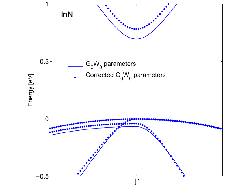
At first glance, the band structures do not differ significantly for both parameter sets. To emphasize the differences, Fig. 2 shows the band structure of InN around the -point. By having a closer look, one can see that the energetic positions are different, because of the different crystal field splitting and band gap. Also, the curvatures of the bands differ for the two parameter sets. This is a result of the slightly different and will be adressed again in Sec. III.2. More sophisticated methods for band structure calculation will give more conduction and valence bands in the energetic range around the band gap. Although this feature could also be included in our EBOM approach by augmenting the number of orbitals per unit cell, it would not only result in a more complicated parametrization, but also lead to significantly higher computational costs for nanostructure calculations. Thus we stick to a minimal basis set of four bands per spin direction, which gives a reasonable agreement with the ”true“ band structure in the region of interest. The reliability of this basis set has also been established by the variety of existing eight-band- calculations for these systems and comparisons to experimental results for device applications. Winkelnkemper et al. (2006, 2007)
Of course, our EBOM parametrization is not limited to a specific set of parameters. The fit to the energies at the BZ boundaries allows for an adaption to a wide range of parameters, as these additional constraints practically prevent spurious solutions where the bands curve into the band gap far away from the BZ center. These problems are widely known to occur for simpler - and tight-binding parametrizations when an inappropriate set of -point parameters is used.
With our model, a more systematic investigation of the influence of single parameters on the properties of low-dimensional systems is possible, as the band structure is not sensitive to small perturbations in the input parameters. This stability of the parametrization transfers directly to the application on nanostructures, as e.g. spurios solutions in the bulk band gap will lead to corresponding states in the forbidden energy region of the nanostructure. In spite of the progress in the field of both sophisticated ab-initio calculations and highly refined experiments, this is and will remain an important feature, as certain physical quantities like band offsets, Luttinger parameters and optical matrix elements remain ambiguous because they are only indirectly measurable and depend on model assumptions.
II.2 Application of the EBOM to quantum dots
As we now have determined the EBOM matrix elements for the bulk materials, they can be used as input in the calculations for a quantum-confined nanostructure. In case of a quantum dot, the translational invariance is lost in all three spatial dimensions, so the adequate ansatz for an eigenstate, Eq. (2), is reduced to a direct linear combination of localized effective orbitals
| (6) |
The corresponding secular equation is now given by
| (7) |
where are the EBOM matrix elements from Eq. (5) and the site indices now range over the finite sites of a sufficiently large supercell. In our present -basis, the eigenstates and eigenenergies of Eq. (7) are obtained as the solutions of a matrix eigenvalue problem. According to Refs. Schulz et al., 2006 and Schulz and Czycholl, 2005, a nanostructure made of one material A embedded in a barrier of material B can be modelled by using the matrix elements of the A-material for the corresponding lattice sites and vice versa. For the interface, a linear interpolation of the corresponding hopping matrix elements is used. The confinement potential for the carriers can properly be incorporated by an upward shifting of the diagonal elements of the A-material by the valence band offset between the two materials. When the band gap between the materials B and A exceeds this offset, we are naturally left with a type-I confinement potential for the electrons and holes.
The application to one- or two-dimensional structures is a trivial task and can be done correspondingly.
II.3 Possible inclusion of piezoelectricity and strain
In the systems under consideration, there is always a spontaneous polarization due to the deviation of the -ratio from the value in the ideal wurtzite structure. Additionally, strain fields will influence the electronic properties of these systems, if present. While there are in fact zero-dimensional systems, like fully relaxed nanocrystals, where this effect can be neglected, the below presented model system of epitaxially grown InN quantum dots embedded in a GaN matrix will in fact be strained due to the lattice mismatch, and this strain will not only shift the band edges, but also alter the equilibrium positions of the lattice sites and thus the piezoelectric charge density.
Both, the spontaneous and the strain induced polarization can be incorporated into the tight-binding calculations by the solution of the Poisson equation. Schulz et al. (2006); Schulz and Czycholl (2006) Although it has been discussed in previous publications like Ref. Schulz et al., 2006, that for this specific quantum dot system a proper inclusion of a constant band-edge shift might be sufficient, a more general approach is of course desirable.
Again, the one-to-one correspondence to the model at allows for a straight-forward inclusion of strain effects on the bulk band structure by augmenting the -Hamiltonian by a strain-dependant part, as done in Refs. Winkelnkemper et al., 2006 and Chuang and Chang, 1996. The then obtained analytical dependance of the EBOM matrix elements on the deformation potentials of the conduction band, of the valence bands and the elastic stiffness constants can then be used either to determine a distance-dependant scaling law for the (similar to the famous Harrison ansatz Froyen and Harrison (1979)) or directly be incorporated into the nanostructure Hamiltonian. In both cases, additionally an appropriate strain field has to be calculated for the low-dimensional system under consideration, either by atomistic Fonoberov and Balandin (2003); Andreev and O’Reilly (2000) or continuum mechanical Winkelnkemper et al. (2006) approaches.
As this extension of the EBOM requires a careful comparison to further experimental and theoretical results, it is a topic of its own and part of ongoing research. Therefore, it will not furtherly be adressed in the present publication. In the following section, we will neglect the influence of piezoelectricity and strain, in order to focus on the direct influence of the slightly different Kane parameters on the single particle results.
III Results for quantum dots
III.1 Model quantum dot geometry
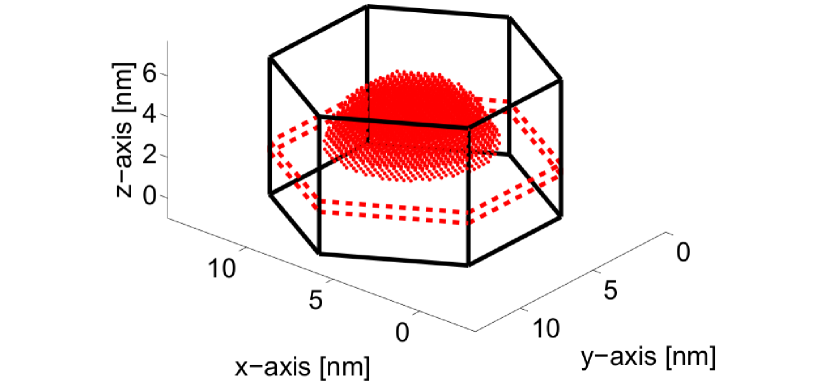
Earlier ETBM calculations of Refs. Schulz et al., 2006, Schulz and Czycholl, 2006 for the InN/GaN material system were performed using cubic supercells and fixed boundary conditions. In this paper we present a different and improved kind of supercell, which is depicted in Fig. 3, by means of keeping the point group symmetry of the underlying hexagonal Bravais lattice in combination with periodic boundary conditions. This leads to several benefits, e.g. no artificial surface states can arise in the single-particle spectrum, and in contrast to cubic supercells our hexagonal one does not interfere with the point group symmetry of the lattice. The simulated lens-shaped InN quantum dot has a diameter of 7.7 nm and a height of 3.1 nm. It is placed on top of a wetting-layer with thickness of one lattice constant, since Stranski-Krastanov growth-mode is assumed for the given structure. The surrounding GaN supercell has a dimension of with respect to the cartesian axes. With this size, convergence for the one-particle wave functions is ensured. Furthermore, a completely strained structure is supposed, so that no deviations from the ideal lattice positions emerge. As valence band offset, we use the value recommended by Vurgaftman et al. Vurgaftman and Meyer (2003) of eV for both parameter sets.
III.2 One-particle spectrum for embedded InN quantum dot
The numerical diagonalization of the corresponding nanostructure Hamiltonian (using the folded spectrum methodWang and Zunger (1994)) gives the desired single-particle states and eigenenergies around the energy gap of the quantum dot. We solve Eq. (7) for eight bound electron and hole states, using the EBOM parametrization for second nearest neighbors and taking spin-orbit coupling and crystal field splitting into account.
parameters
 Corrected parameters

The resulting eigenfunctions are visualized in Fig. 4 by isosurfaces of the probability density, supplemented by the respective eigenenergies. All states are invariant under rotations by around the growth direction, according to the point group symmetry of the Bravais lattice. Each state is once again twofold degenerate due to time-reversal symmetry and well localized within the InN quantum dot. Tab. 3 reveals that the electron states mainly stem from the -like conduction band, so a classification by their nodal structure is possible. is -like, while and are complex linear combinations of the form . is a -like state, but distorted by the shape of the quantum dot. The hole states show similar transformation properties at first glance. Nevertheless, Tab. 3 reveals that at least two atomic -states contribute to their formation, so that they underlie strong band-mixing effects. This is in agreement with results from several other multiband calculations. Wei and Zunger (1996); Fonoberov and Balandin (2003)
| parameters | ||||||||
|---|---|---|---|---|---|---|---|---|
| 0.878 | 0.839 | 0.839 | 0.843 | 0.000 | 0.004 | 0.002 | 0.001 | |
| 0.033 | 0.056 | 0.056 | 0.034 | 0.499 | 0.492 | 0.494 | 0.495 | |
| 0.033 | 0.056 | 0.056 | 0.034 | 0.499 | 0.492 | 0.494 | 0.495 | |
| 0.057 | 0.049 | 0.049 | 0.088 | 0.001 | 0.012 | 0.010 | 0.009 | |
| Corrected parameters | ||||||||
|---|---|---|---|---|---|---|---|---|
| 0.858 | 0.812 | 0.812 | 0.818 | 0.005 | 0.000 | 0.004 | 0.001 | |
| 0.036 | 0.063 | 0.063 | 0.032 | 0.490 | 0.497 | 0.491 | 0.490 | |
| 0.036 | 0.063 | 0.063 | 0.032 | 0.490 | 0.497 | 0.491 | 0.490 | |
| 0.070 | 0.063 | 0.063 | 0.118 | 0.014 | 0.003 | 0.015 | 0.019 | |
By taking a closer look at the degeneracies in Fig. 4, we notice no fourfold degeneracy of and , in contrast to -calculations from Ref. Winkelnkemper et al., 2006, but reproduce the findings of earlier ETBM calculations from Ref. Schulz et al., 2008, showing a twofold degeneracy for each bound state. The latter reference also includes a detailed group theoretical dicussion of this issue. The only deviations we can report on is the fact that the EBOM eigenenergies of the electrons are more strongly bound for both parameter sets, compared to other ETBM results from Refs. Schulz et al., 2006 and Schulz and Czycholl, 2006. This discrepancy can safely be attributed to the once again different set of input parameters and thus does not contradict comparative studies from Refs. Marquardt et al., 2008 and Schulz et al., 2009 for zincblende nanostructures, which show a very good agreement between these approaches. Our results for the hole energies agree well with the earlier calculations of Refs. Schulz et al., 2006 and Schulz and Czycholl, 2006 if the piezoelectric field is neglected (see e.g. Ref. Schulz et al., 2006 for details).
A striking feature is the different order of the hole levels when switching between the parameter sets. The torus-shaped probability density belongs to the hole ground state with the parameters, but is found as the first excited hole state when using the corrected parameters. Another look at Tab. 2 reveals that the band gap of the dot material differs by less than meV between these parameter sets; the confinement potential for the holes is even identical in both cases, as the same valence band offset is used. The crystal field splitting only differs by ca. meV for both materials. Obviously, this rather small variation of the bulk band gap and the crystal field splitting, which also results in slightly different Kane parameters (see App. A), suffices to change the level structure. Further studies (not shown) reveal that even variations in the order of magnitude of the accuracy of the input parameters can change the order. In addition, the differing bulk band gaps of the two parameter sets lead to slightly different one-particle energy gaps of eV ( parameters) and eV (corrected parameters), respectively. When calculating optical properties like the excitonic absorption spectrum from the tight-binding single-particle spectrum, as e.g. done in Refs. Schulz et al., 2006 and Schulz et al., 2009, the level structure and are important characteristics. A change in the first will give rise to a change of the respective dipole matrix elements between the electron and hole states and thus alter the line intensity, while a change in directly shifts the energetic position of the line itself.
As the variation of the dot size and the proper implementation of strain effects and electrostatic built-in fields can additionally alter the level ordering, the influence of different material parameters should be carefully investigated when discussing the optical selection rules for a given geometry. For the system under consideration, we recommand the use of the corrected parameters.
IV Conclusion and outlook
In this paper, we have presented a multiband empirical tight-binding parametrization for both bulk semiconductors and nanostructures with a wurtzite structure, which represents an adaption of the effective bond-orbital model (EBOM) for the hexagonal phase. A basis set of one - and three -orbitals for each spin direction is placed on the sites of the underlying hexagonal Bravais lattice. Coupling up to second nearest neighbors has been used to fit one conduction and three valence bands to the energies and curvatures at the -point and, additionally, to the energies at high symmetry points throughout the whole Brillouin zone. The resulting band structures of the III-V-compounds InN, GaN and AlN were shown for two disctinct parameter sets, namely the newest - results by Rinke et al. and a slightly modified set, in which we adjusted single critical parameters by replacing them by the values given by Vurgaftman et al. in order to obtain better agreement to experimental results.
In addition, we demonstrated the application of this parametrization to low-dimensional structures. A lens-shaped InN quantum dot on an InN wetting layer, embedded in a GaN matrix, has been modelled within a hexagonally shaped supercell with periodic boundary conditions. We have compared the resulting one-particle spectrum and the corresponding eigenstates to previous tight-binding results and have found a good concordance within the framework of the respective model. Furthermore, we have found that the two parameter sets yield a different order of hole states for the given dot diameter, although the corresponding bulk band structures barely differ at first glance. We strongly approve a careful review of the set of material parameters used in such calculations. For the present InN/GaN quantum dot system, we recommend the use of the corrected parameter set.
Besides the application to other quantum dot systems, like GaN in AlN, or different geometries, like coupled QDs or spherical nanocrystals, the present parametrization can easily be applied to one-dimensional (quantum wires) or two-dimensional (quantum wells and superlattices) structures. Moreover, the effects of strain and piezoelectric built-in fields can be incorporated on different levels of sophistication, as suggested in the second section of this publication.
Acknowledgements.
The authors would like to thank Patrick Rinke for the provision of additional results at further high symmetry points of the Brillouin zone. Furthermore, we thank Stefan Schulz for fruitful discussions. This work has been supported by the Deutsche Forschungsgemeinschaft (research group “Physics of nitride-based, nanostructured, light-emitting devices”, project Cz 31/14-3).Appendix A EBOM parametrization for the hexagonal lattice
The analytical dependance of the parameters
| (8) |
of the band gap , the spin-orbit and crystal field splittings and the effective masses is given by the following two equations: Chuang and Chang (1996)
| (9) |
| (10) |
The EBOM parametrization scheme with coupling up to second nearest neighbors gives a set of equations which link the parameters of Tab. 2 to the EBOM matrix elements of Eq. 5. To obtain the desired number of free parameters for a one-to-one correspondance, one has to apply an adequate decomposition of the into two- and three-center integrals, following the guidelines of Ref. Slater and Koster, 1954. As the explicit solution is straightforward, but very unhandy in print, it shall not be given here in full form. Instead, further details will be made accessible as supplementary material to this publication in mathematical notation in Ref. sup, 2010a and, additionally, the explicit solution as MATLAB-compatible pseudocode in Ref. sup, 2010b, so that it can easily be used for own computations.
In order to give at least a brief insight into the physical meaning of the , we will give the results of the expansion of Eq. (4) to second order in . In this limit, the EBOM and the -presentation become equivalent. The following set of equations gives the EBOM matrix elements in terms of the parameters that were used in the 8-band--Hamiltonian of Refs. Winkelnkemper et al., 2006 and Chuang and Chang, 1996, where the are Luttinger-like parameters which are connected to the anisotropic effective valence band masses. For the sake of simplicity, the parameter has been set to zero in our approach. Its influence has turned out to be negligible. Dugdale et al. (2000) The upper index in now denotes in units of half the lattice constants or , respectively, so that
| (11) | |||||
References
- Guzelian et al. (1996) A. A. Guzelian, U. Banin, A. V. Kadavanich, X. Peng, and A. P. Alivisatos, Appl. Phys. Lett. 69, 1432 (1996).
- Michler (2009) P. Michler, Single Semiconductor Quantum Dots (Springer, 2009), 1st ed.
- Bruchez et al. (1998) M. Bruchez, M. Moronne, P. Gin, S. Weiss, and A. P. Alivisatos, Science 281, 2013 (1998).
- Michalet et al. (2005) X. Michalet, F. F. Pinaud, L. A. Bentolila, J. M. Tsay, S. Doose, J. J. Li, G. Sundaresan, A. M. Wu, S. S. Gambhir, and S. Weiss, Science 307, 538 (2005).
- Lazar et al. (2004) S. Lazar, C. Hébert, and H. W. Zandbergen, Ultramicroscopy 98, 249 (2004).
- Grundmann et al. (1995) M. Grundmann, O. Stier, and D. Bimberg, Phys. Rev. B 52, 11969 (1995).
- Wojs et al. (1996) A. Wojs, P. Hawrylak, S. Fafard, and L. Jacak, Phys. Rev. B 54, 5604 (1996).
- Shi and Gan (2003) J. Shi and Z. Gan, J. Appl. Phys. 94, 407 (2003).
- Fonoberov and Balandin (2003) V. A. Fonoberov and A. A. Balandin, J. Appl. Phys. 94, 7178 (2003).
- Pryor (1998) C. Pryor, Phys. Rev. B 57, 7190 (1998).
- Stier et al. (1999) O. Stier, M. Grundmann, and D. Bimberg, Phys. Rev. B 59, 5688 (1999).
- Andreev and O’Reilly (2000) A. D. Andreev and E. P. O’Reilly, Phys. Rev. B 62, 15851 (2000).
- Wang and Zunger (1996) L. W. Wang and A. Zunger, Phys. Rev. B 53, 9579 (1996).
- Wang and Zunger (1999) L. W. Wang and A. Zunger, Phys. Rev. B 59, 15806 (1999).
- Wang et al. (2000) L. W. Wang, A. J. Williamson, A. Zunger, H. Jiang, and J. Singh, Appl. Phys. Lett. 76, 339 (2000).
- Bester and Zunger (2005) G. Bester and A. Zunger, Phys. Rev. B 71, 045318 (2005).
- Santoprete et al. (2003) R. Santoprete, B. Koiller, R. B. Capaz, P. Kratzer, Q. K. K. Liu, and M. Scheffler, Phys. Rev. B 68, 235311 (2003).
- Schulz and Czycholl (2005) S. Schulz and G. Czycholl, Phys. Rev. B 72, 165317 (2005).
- Schulz et al. (2006) S. Schulz, S. Schumacher, and G. Czycholl, Phys. Rev. B 73, 245327 (2006).
- Schulz and Czycholl (2006) S. Schulz and G. Czycholl, phys. stat. sol. (c) 3, 1675 (2006).
- Schulz et al. (2008) S. Schulz, S. Schumacher, and G. Czycholl, The European Physical Journal B 64, 51 (2008).
- Korkusinski et al. (2008) M. Korkusinski, P. Hawrylak, M. Zielinski, W. Sheng, and G. Klimeck, Microelectronics Journal 39, 318 (2008).
- Rinke et al. (2006) P. Rinke, M. Scheffler, A. Qteish, M. Winkelnkemper, D. Bimberg, and J. Neugebauer, Appl. Phys. Lett. 89, 161919 (2006).
- Rinke et al. (2008) P. Rinke, M. Winkelnkemper, A. Qteish, D. Bimberg, J. Neugebauer, and M. Scheffler, Phys. Rev. B 77, 075202 (2008).
- Slater and Koster (1954) J. C. Slater and G. F. Koster, Phys. Rev. 94, 1498 (1954).
- Chang (1988) Y. C. Chang, Phys. Rev. B 37, 8215 (1988).
- Loehr (1994) J. P. Loehr, Phys. Rev. B 50, 5429 (1994).
- Fritsch et al. (2004) D. Fritsch, H. Schmidt, and M. Grundmann, Phys. Rev. B 69, 165204 (2004).
- Chen (2004) C. Chen, Physics Letters A 329, 136 (2004).
- Cartoixá et al. (2003) X. Cartoixá, D. Z. -Y. Ting, and T. C. McGill, Phys. Rev. B 68, 235319 (2003).
- Chadi (1977) D. J. Chadi, Phys. Rev. B 16, 790 (1977).
- Winkelnkemper et al. (2006) M. Winkelnkemper, A. Schliwa, and D. Bimberg, Phys. Rev. B 74, 155322 (2006).
- Chuang and Chang (1996) S. L. Chuang and C. S. Chang, Phys. Rev. B 54, 2491 (1996).
- Yeo et al. (1998) Y. C. Yeo, T. C. Chong, and M. F. Li, J. Appl. Phys. 83, 1429 (1998).
- Rinke et al. (2005) P. Rinke, A. Qteish, J. Neugebauer, C. Freysoldt, and M. Scheffler, New Journal of Physics 7, 126 (2005), ISSN 1367-2630.
- Rinke (2009) P. Rinke, obtained by private communication (2009).
- Vurgaftman and Meyer (2003) I. Vurgaftman and J. R. Meyer, J. Appl. Phys. 94, 3675 (2003).
- Winkelnkemper et al. (2007) M. Winkelnkemper, R. Seguin, S. Rodt, A. Schliwa, L. Reissmann, A. Strittmatter, A. Hoffmann, and D. Bimberg, J. Appl. Phys. 101, 113708 (2007).
- Wang and Zunger (1994) L. Wang and A. Zunger, The Journal of Chemical Physics 100, 2394 (1994).
- Wei and Zunger (1996) S. Wei and A. Zunger, Appl. Phys. Lett. 69, 2719 (1996).
- Marquardt et al. (2008) O. Marquardt, D. Mourad, S. Schulz, T. Hickel, G. Czycholl, and J. Neugebauer, Phys. Rev. B 78, 235302 (2008).
- Schulz et al. (2009) S. Schulz, D. Mourad, and G. Czycholl, Phys. Rev. B 80, 165405 (2009).
- sup (2010a) See supplementary document supplementary_material.pdf for further details of the parametrization.
- sup (2010b) See supplementary file ebom_integrals_snn.txt for the explicit solution of the resulting system of equations.
- Dugdale et al. (2000) D. J. Dugdale, S. Brand, and R. A. Abram, Phys. Rev. B 61, 12933 (2000).
- Froyen and Harrison (1979) S. Froyen and W. A. Harrison, Phys. Rev. B 20, 2420 (1979).