Deformation potentials and electron-phonon coupling in silicon nanowires
Abstract
The role of reduced dimensionality and of the surface on electron-phonon (e-ph) coupling in silicon nanowires is determined from first principles. Surface termination and chemistry is found to have a relatively small influence, whereas reduced dimensionality fundamentally alters the behavior of deformation potentials. As a consequence, electron coupling to ‘breathing modes’ emerges that can not be described by conventional treatments of e-ph coupling. The consequences for physical properties such as scattering lengths and mobilities is significant: the mobilities for [110] grown wires is 6 times larger than for [100] wires, an effect that can not be predicted without the form we find for Si nanowire deformation potentials.
Silicon nanowires, beyond having been successfully demonstrated as conventional semiconductor devices 1, 2, 3, 4, are beginning to be seen as the important blocks for novel energy harvesting applications, such as solar cells 5, 6 and efficient thermoelectric devices 7, 8. All these applications rely on a high electronic conductivity of electrons, while in the latter a low phonon conductivity is also essential 9, 10. At the heart of understanding the interrelation between these properties is the interaction of phonons and electrons: scattering of electrons with phonons reduces the conductivity of these devices, increasing heating and reducing their efficiency, while the scattering of phonons with electrons reduces thermal conductivity, yielding better thermoelectric attributes. But although electron-phonon coupling in bulk semiconductors has been extensively studied, the nanoscale regime is not so well understood.
Materials when structured as low-dimensional systems are known to exhibit new behavior relative to their macroscopic properties. In the case of silicon nanowires, quasi-one dimensional structures, band folding can result in an electronic structure with a direct band gap. The Increased surface to volume ratio permits the surface chemistry to significantly alter the value of band gaps 11, 12. In this paper, we demonstrate that reduced dimensionality in silicon nanowires also has a significant impact on electron-phonon (e-ph) interactions that has not been previously anticipated. We derive a new form for deformation potentials in Si nanowires that enables a general approach to the calculation of e-ph couplings, an approach that may be readily extended to other semiconductor nanowires. The validity of such macroscopic theories at the nanoscale is central to advancing semiconductor technology (see, e.g., the developments in the effective mass approximation 13, 14, 15). To our knowledge, this is the first paper to address the effects of dimensionality on the deformation potential theory.
For this purpose, we employ density functional theory (DFT) to calculate the band structure of Si nanowires and apply strain to extract the deformation potentials. DFT is known to give good agreement with experiments of the band gap pressure dependence16, 17 and to give accurate deformation potentials that reproduce the n-type carrier mobility in bulk18. Focusing on electrons, we find that contrary to common assumption, the tabulated deformation potentials not only vary as a function of size and orientation but also vary with respect to the direction of the applied strain. This has a direct influence on the strength of the scattering of electrons by phonons travelling in different directions. We develop a simple theory to take into account the full anisotropy of the deformation potentials and its impact on electron mobility. The effect of the direction of growth of the wires and surface passivation is also studied. Notably, the deformation potentials in [110]-oriented wires are found to be highly anisotropic when compared to those of [100] wires or bulk silicon. This results in the suppression of the scattering from breathing modes, and, coupled to their lower effective mass, leads to much higher mobilities for [110] wires.
Electron-phonon coupling in nanowires can be expressed in a similar manner to the deformation potential theory for anisotropic scattering in multi-valley semiconductors 19. A first approximation might be to use the bulk values for the deformation potentials to determine an isotropic model independent of the nanowire diameter or surface termination together with the effective masses calculated for specific nanowires. Unfortunately, as Leu et al 20 find in their recent paper, the deformation potentials of the valence and conduction bands of and Si nanowires are substantially different from those in bulk Si for strains applied along the nanowire axis. A common practice is to assume an isotropic e-ph scattering rate with an effective value to account for deformation potential variations in nanowires relative to bulk 21, 22, 23, greatly simplifying the calculation of physical quantities derived from the deformation potential. Speaking against this approach is the fact that Fischetti and Laux 24 have shown that the anisotropy of the e-ph matrix element has a substantial effect on the magnitude of the electron-phonon scattering rate in a 2D electron gas in silicon.
The effect of an acoustic phonon on the electronic band structure is equivalent to that produced by a slowly varying strain in the direction of the phonon. This strain introduces a correspondent slowly varying potential that scatters the electrons. The change in the energy of a band per unit of strain is called a deformation potential. The deformation potential theory for bulk semiconductors has been developed by Herring and Vogt 19, who find the anisotropic electron-acoustic phonon matrix element for an elliptical valley in silicon to be:
| (1) |
where and are the dilatation and the uniaxial-shear deformation potentials, respectively, is the phonon momentum, is a unit vector parallel to the k-vector of valley and is the amplitude of the displacement of the atoms due to a phonon with polarization . We will initially assume that this theory still holds for SiNWs, and find and from electronic structure calculations. Our assumption will hold for wires with large enough diameter D. For quasi-one dimensional nanowires (D nm) 25, we show that corrections are needed. It will be seen that, for the quasi-one dimensional wires, becomes anisotropic with respect to the direction of the applied strain (or phonon); this effect is particularly pronounced for -SiNWs.
The band structure of nanowires can be understood to be due to the spatial confinement of the bulk electronic bands. For a nanowire, the indirect conduction band (CB) minimum at is formed by the bulk Si valleys at , with energy , where . The CB minima at are composed from the four valleys at and , with energies and , respectively. From explicit band calculations for a nanowire, the four valleys that fold into are not exactly degenerate owing to level splitting introduced by the surface. We can use a simple theory in which the effect of the surface is to introduce interactions between four degenerate bands, so that the CB minima in the SiNW can be described by the eigenvalues of the following matrix,
| (2) |
where and are the g-type and f-type matrix elements between the bulk-like bands, respectively, introduced by the presence of the surface. The four eigenvalues of this matrix are
| (3) | |||||
| (4) |
In the absence of strain, , and are degenerate and , which we find to hold for hydrogenated SiNWs 26. Similarly, in a nanowire, the conduction band minimum is at and formed from the bulk valleys at , with energy and the band minimum close to , is formed by the bulk valleys and , with energies and . The effective mass of the lowest conduction band in the wires is thus given by the transverse mass in bulk, while the subband separation depends on the longitudinal mass. The effective masses are directly calculated for the wires from first principles (see 1). The meaning of the effective masses and for the wires is as follows: is the effective mass along the direction of the wire, since, from an effective mass perspective, the lowest conduction band can be considered as formed by the valleys with transverse mass along the direction of the wire. Likewise, is such that it gives the correct separation between the first sub-bands.
The valleys shift according to Eq. (1) as strain is applied, yielding the deformation potentials for each of the NW bands. From these shifts and Eqns. (3) and (4), we can obtain and . For example, a strain in the direction yields, where are the deformation potentials corresponding to the bands. The variation of and due to strain is found to be small and is ignored in the following. The resulting values for the wires studied in this work are shown in 1.
| Width [nm] | Atoms/cell | [eV] | [eV] | [eV] | [eV] | [eV] | ||
|---|---|---|---|---|---|---|---|---|
| 0.82 | [100] | 0.46 | 1.4 | -0.3 | 0.038 | -4.2 | -4.2 | 8.2 |
| 0.77 | [100] | 0.37 | 0.9 | -0.039 | 0.009 | -6.1 | -6.1 | 8.7 |
| 1.09 | [100] | 0.44 | 1.1 | 0.078 | 0.025 | -4.7 | -4.7 | 8.6 |
| 1.26 | [100] | 0.4 | 1.1 | -0.074 | 0.017 | -5.5 | -5.5 | 9.2 |
| 1.9 | [100] | 0.39 | 1.1 | -0.047 | 0.0026 | -6.6 | -6.6 | 9.2 |
| 1.086 | [100] | 0.72 | 0.95 | 0.24 | 0.05 | -4.8 | -6.5 | 5.3 |
| 0.53 | [110] | 0.15 | 1.5 | 0.58 | -9.4 | -1.3 | 3.7 | |
| 1.09 | [110] | 0.15 | 0.62 | 0.38 | -10.0 | -1.8 | 3.7 | |
| 1.15 | [110] | 0.15 | 0.62 | 0.39 | -9.1 | -0.1 | 3.9 | |
| 1.35 | [110] | 0.15 | 0.62 | 0.21 | -10.5 | -1.3 | 4.1 | |
| 3.07 | [110] | 0.15 | 0.62 | 0.018 | -9.5 | -3.3 | 5.8 | |
| 1.15 | [110] | 0.19 | 0.95 | 0.03 | -7.5 | -3.2 | 3.1 | |
| 1.35 | [110] | 0.15 | 0.95 | 0.33 | -7.3 | -5.1 | 3.9 |
We have calculated27 the deformation potentials for the first conduction bands for wires of different sizes with orientations and , by varying the interatomic distance by 0.1% to 0.5% along and perpendicular to the wire axis. 1 shows the and calculated using the values from the lowest bands at . Here, and are the equivalent of the deformation potential in the parallel and perpendicular directions to the wire axis, respectively. From these direct band structure calculations, we have found that Eq. (1) still holds for small nanowires, except for hydroxylated and [110] wires, where the expression can be corrected to include the anisotropy due to the breaking of bulk symmetry, as seen below. Surprisingly, there is very little variation in the and bulk-like deformation potentials with the strain direction in the wires, and has the same value as bulk silicon18. On the other hand, varies substantially with strain direction in the wires, and is half its value in bulk. The anisotropy in can be accounted for in Eq. (1), by interpolating this deformation potential as a function of strain direction as follows,
| (5) |
where the are the cartesian components of the dimensionless unit vector along the phonon momentum.
In what follows, we use the values of 1 and the Boltzmann transport equation to estimate the mobility of the SiNWs. The momentum relaxation time, , due to acoustic phonon scattering can be expressed as
| (6) | |||||
where the upper and lower symbols in “” indicate the emission or absorption of a phonon, are the dimensions of a wire of rectangular cross section, with the periodic direction, is the velocity of carriers with momentum , the polarization of a phonon with momentum in branch , and
| (7) | |||||
is the overlap factor of the wavefunctions (see Note 25 for the meaning of the indices and vectors in this context). The choice of “effective mass” wavefunctions for Eq. (7) over the Kohn-Sham wavefunctions is based on ease of use and to simplify the understanding of the different contributions to the scattering from the different modes. This approximation should work for large wires. In smaller wires, the electron confinement and the matrix elements introduced by the surface push five of the six sub-bands up in energy, beyond the range of acoustic phonon scattering at room temperature. As a result, this approximation works well for the lowest sub-band, which is the main contributor the the mobility. Some corrections should be expected for the scattering into higher sub-bands, but they are not important for the cases considered in this work. We therefore expect the main difference in comparing the different wires to come from the deformation potentials. Eq. (6) can be solved numerically, and using the elastic approximation does not yield noticeable differences. The acoustic phonon-limited mobility can then be obtained as where is the effective mass of a carrier in the conduction band. Thanks to the breaking of the degeneracy of the conduction bands due to the surface matrix elements and confinement observed, we expect the contribution from optical and intervalley to be small for the range of energies considered in this work. We would like to point out that, while we have used the bulk phonon dispersions, discretised perpendicular to the wire axis, the effect of the full deformation potential remains the same, and we do not expect a large difference in the mobilities between this approach and using the phonon band structure of the wires28.
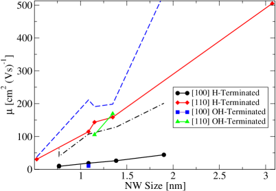
The room temperature mobilities ) of wires with varying orientation and surface termination versus wire size are summarised in 1 where it is seen that the nanowire orientation has a much larger effect on electron mobility than surface passivation. Due to the increased effective mass, OH surface passivation affects only the [100] growth orientation, halving the mobility compared to H-passivation for the case considered. A lower mobility is observed for the -oriented wires compared to the -SiNWs. One factor yielding the lower mobilities for wires is their larger electron effective masses (see 1). However, the electron relaxation times in the and wires differ fundamentally in that the e-ph coupling for breathing vibrational modes in the nanowires are suppressed relative to the wires or bulk silicon. For the wires, electron scattering due to the phonon modes along the wire axis is usually more than four times as strong as that due to the modes perpendicular to the wire axis (breathing modes), and larger than for the wires. In the latter, however, the scattering is more isotropic, with the result that breathing modes have similar e-ph coupling strengths as for excitation of modes along the wire axis. To demonstrate the importance of the breathing modes in suppressing the -mobility, in 1 we consider the effect of de-coupling the breathing modes from the scattering matrix. As the nanowire diameter is increased, coupling to the breathing modes play an increasingly important role in determining the electron mobility.
The anisotropy in the deformation potentials is also expected to influence the thermoelectric performance of NWs. The electrical conductivity and the electronic and phonon thermal conductivity that determine the figure of merit (, where and are the ionic and electronic thermal conductivities, respectively, is the electronic conductivity, the Seebeck coefficient, and is the temperature), will depend on several factors such as temperature, impurity concentration, surface roughness and chemistry. Considering the effect of the anisotropic potentials alone, better performance is expected for the [110] NWs compared to the [100] or bulk silicon: the enhanced scattering of the phonons by electrons along the direction of the wires (i.e. the direction of the thermal gradient) decreases thermal conductivity, while the overall reduction of the scattering of electrons by breathing modes enhances the electronic mobility. Hence, these two effects combined should result in a higher figure of merit for the [110] NW.
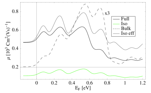
We would like highlight the consequences of attempting to apply bulk-like deformation potential models to calculate the electron mobility in SiNWs. In 2, we show the room temperature mobility versus the Fermi energy for a wire of 3 nm diameter oriented along a Si direction, computed using the deformation potentials calculated in this work and compared to the mobility calculated using eV and eV, from Ref.18 for bulk silicon. The mobility obtained by using bulk deformation potential values underestimates the scattering by longitudinal phonons along the wire direction resulting in a significant overestimation of the electron mobility. It has been argued22 that it is possible to build an approximation by which the value of an isotropic deformation potential reproduces the universal mobility curve obtained from wires of large diameter. However, this approach underestimates the electron mobility relative to the use of the explicit model developed in this work, as displayed by the green curve (labeled Iso) in 2. Alternatively, to determine whether we can apply an isotropic model to reproduce the calculated mobility, we may attempt to define an effective isotropic deformation potential
| (8) |
that, used with an isotropic version of Eq. (6) (with the longitudinal phonon branch only) reproduces the anisotropic mobility at . The mobility obtained in this manner is also plotted in 2. We find that the isotropic model is still not adequate in this case, where is highly anisotropic, and is smaller or near . Nevertheless, an isotropic model will work when the condition is satisfied, as is the case of the silicon nanowires oriented along a direction.
In summary, we have calculated from first-principles the deformation potential of nanowires of different diameters, with and orientations and for hydrogen and hydroxyl surface termination, and extended the deformation potential theory to develop for the first time a model that incorporates the effects of lower dimensionality in the electron phonon scattering rate. While we find that surface termination changes the bands substantially12, 11, it has little effect on the deformation potentials. To the contrary, we find that the deformation potentials in are highly anisotropic, in contrast to those of wires and bulk silicon. This effect results in the suppression of the scattering from breathing modes in wires, which, added to their lower effective mass, leads to a greater n-type carrier mobility compared to [100]-oriented wires.
This material is based upon works supported by the Science Foundation Ireland under Grant No. 06/IN.1/I857, and the European Union project Nanosil. We would like to thank Stephen Fahy and Baruch Feldman for useful comments on the manuscript.
References
- Cui et al. 2003 Cui, Y.; Zhong, Z. H.; Wang, D. L.; Wang, W. U.; Lieber, C. M. Nano Lett. 2003, 3, 149
- Cui and Lieber 2001 Cui, Y.; Lieber, C. M. Science 2001, 291, 851
- Duan et al. 2001 Duan, X. F.; Huang, Y.; Cui, Y.; Wang, J. F.; Lieber, C. M. Nature 2001, 409, 66
- Goldberger et al. 2006 Goldberger, J.; Hochbaum, A. I.; Fan, R.; Yang, P. Nano Lett. 2006, 6, 973
- Tian et al. 2007 Tian, B.; Zheng, X.; Kempa, T. J.; Fang, Y.; Yu, N.; Yu, G.; Huang, J.; Lieber, C. M. Nature 2007, 449, 885
- Tsakalakos et al. 2007 Tsakalakos, L.; Balch, J.; Fronheiser, J.; Korevaar, B. A.; Sulima, O.; Rand, J. Appl. Phys. Lett. 2007, 91, 233117
- Boukai et al. 2008 Boukai, A. I.; Bunimovich, Y.; Tahir-Kheli, J.; Yu, J. K.; Goddard, W. A.; Heath, J. R. Nature 2008, 451, 168
- Hochbaum et al. 2005 Hochbaum, A.; Fan, R.; He, R. R.; Yang, P. D. Nano Lett. 2005, 5, 457
- Vo et al. 2008 Vo, T. T. M.; Williamson, A. J.; Lordi, V.; Galli, G. Nano Lett. 2008, 8, 1111
- Shi et al. 2009 Shi, L.; Yao, D.; Zhang, G.; Li, B. Appl. Phys. Lett. 2009, 95, 063102
- Leu et al. 2006 Leu, P. W.; Shan, B.; Cho, K. Phys. Rev. B 2006, 73, 195320
- Nolan et al. 2007 Nolan, M.; O’Callaghan, S.; Fagas, G.; Greer, J. C.; Frauenheim, T. Nano Lett. 2007, 7, 34
- Wang et al. 2005 Wang, J.; Rahman, A.; Ghosh, A.; Klimeck, G.; Lundstrom, M. IEEE TRANSACTIONS ON ELECTRON DEVICES 2005, 52, 1589
- Sajjad et al. 2009 Sajjad, R. N.; Alam, K.; Khosru, Q. D. M. Semicond. Sci. Technol. 2009, 24, 045023
- Esposito et al. 2009 Esposito, A.; Luisier, M.; Frey, M.; Schenk, A. Solid-State Electronics 2009, 53, 376
- Chang et al. 1984 Chang, K.; Froyen, S.; Cohen, M. L. Solid State Commun. 1984, 50, 105
- Zhu et al. 1989 Zhu, X.; Fahy, S.; Louie, S. G. Phys. Rev. B 1989, 39, 7840
- Murphy-Armando and Fahy 2008 Murphy-Armando, F.; Fahy, S. Phys. Rev. B 2008, 78, 035202
- Herring and Vogt 1956 Herring, C.; Vogt, E. Phys. Rev. 1956, 101, 944
- Leu et al. 2008 Leu, P. W.; Svizhenko, A.; Cho, K. Phys. Rev. B 2008, 77, 235305
- Zou and Balandin 2000 Zou, J.; Balandin, A. Jour. App. Phys. 2000, 89, 2932
- Jin et al. 2007 Jin, S.; Fischetti, M. V.; Tang, T. Jour. App. Phys. 2007, 102, 083715
- Ramayya et al. 2008 Ramayya, E. B.; Vasileska, D.; Goodnick, S. M.; Knezevic, I. Journal of Applied Physics 2008, 104, 063711
- Fischetti and Laux 1992 Fischetti, M. V.; Laux, S. E. Phys. Rev. B 1992, 48, 2244
- 25 The phonon- and electronic-wavefunctions become confined in the directions perpendicular to the growth direction of the wire. The phonon and electron momentum thus become discretised in these directions, yielding respectively and , where , and . Here, confinement to phonons with bulk dispersion is applied.
- 26 DFT calculations were performed using the Quantum-Espresso package.29 We used the local density approximation for exchange and correlation, and norm conserving pseudopotentials generated by Von Barth-Car. A cut off energy of 408 eV for the plane-wave expansion and a Monkhorst-Pack point number of 4 along the NW growth direction are sufficient converge all paramenters within the significant figures presented. The interwire distance is no less than 1nm, such that there is no significant overlap between the wavefunctions of neighbouring wires in a supercell. Structures were optimized such that the force on each atom is smaller than Ryd/Bohr.
- 27 To obtain the band shifts with strain, and hence the deformation potentials, we subtract the band eigenvalue of the unstrained cell from that of the strained cell, using two different unit cell calculations. To define a reference potential, we ensure that the average of the local potential is the same for both cells in the vacuum outside the nanowire.
- 28 We have performed calculations using the correct phonon dispersions for the [110] 1.15nm wire and for the [100] 1.09nm wire, and found the mobilities to be up to 30 higher in both cases, when compared to using the discretised bulk phonon dispersions. The effect of the deformation potentials remains unchanged, and the comparison between the two wire orientations remains valid.
- Baroni et al. http://www.pwscf.org/ Baroni, S.; Corso, A. D.; de Gironcoli, S.; Giannozzi, P.; Cavazzoni, C.; Ballabio, G.; Scandolo, S.; Chiarotti, G.; Focher, P.; Pasquarello, A.; Laasonen, K.; Trave, A.; Car, R.; Marzari, N.; Kokalj, A. http://www.pwscf.org/