Impact of dimerization and stretching on the transport properties of molybdenum atomic wires
Abstract
We study the electrical and transport properties of monoatomic Mo wires with different structural characteristics. We consider first periodic wires with inter-atomic distances ranging between the dimerized wire to that formed by equidistant atoms. We find that the dimerized case has a gap in the electronic structure which makes it insulating, as opposed to the equidistant or near-equidistant cases which are metallic. We also simulate two conducting one-dimensional Mo electrodes separated by a scattering region which contains a number of dimers between 1 and 6. The characteristics strongly depend on the number of dimers and vary from ohmic to tunneling, with the presence of different gaps. We also find that stretched chains are ferromagnetic.
pacs:
73.63.-b, 72.60+g, 31.15.A-, 73.23.AdI Introduction
The field of Nanoelectronics has emerged as one of the most important branches of Nanoscience and Nanotechnology, due to both the fundamental quantum phenomena occurring at this scale and to its technological relevance in the context of miniaturization and performance improvement of electronic devices. Remarkable progress in the experimental techniques, achieved during the last years, for growing, manipulating and measuring at the nanoscale has allowed to demonstrate several prototype devices such as conducting wires, point contacts and switches.nitzan
Metallic atomic-scale nanowires, in particular, have attracted considerable efforts devoted to their production and isolation.benz ; zach ; nilius Also infinite monoatomic wires have been theoretically investigated recently in order to better understand the magnetic and transport properties of one-dimensional atomic contacts.autes ; miura ; tosatti ¿From such idealized models we can gain valuable information which can be compared later with the realistic systems to get insight in the influence of defects, impurities, host material or the structure of the contacts.
Understanding the transport properties like the current flow through these nanoscale devices, has been a challenge from the theoretical side due to the non-equilibrium quantum kinetic description required. The modern theory of quantum transport is based on the scattering theory or on the Keldysh-Kadanoff-Baym non-equilibrium Green’s function (NEGF) formalism.datta The SMEAGOL codesmeagol ; towards is a flexible and efficient implementation of the NEGF formalism. SMEAGOL obtains the Hamiltonian from the density functional theory (DFT)kohn-sham code SIESTA,siesta which uses pseudopotentials and a localized basis set of pseudo-atomic orbitals, and calculates self-consistently the density matrix, the transmission and the current for each bias voltage.
Very recently, individual molybdenum chains have been produced and controlled by encapsulating them inside carbon nanotubes.muramatsu Mo is indeed an interesting metal element as regards its ability to form one-dimensional (1D) structures, even in free environment. Recent ab-initio calculations of free-standing Mo atomic clusters have shown that linear atomic chains containing up to four atoms are considerably more stable than two- and three- dimensional structuresfaustino . This result is relevant in the context of Mechanically Controllable Break Junction experiments (MCBJE), where atomic chains are fabricated at ultra-low temperatures by bending and eventually breaking up an atomic strip. Interestingly, only the elements gold, platinum and iridium have been found to make them,smit although other elements like Sn could be possible candidates.lucas . Due to its tendency to make linear clustersfaustino Molybdenum could also be used to make atomic chains in MCBJE. Therefore, a transport calculation of such chains is indeed timely.
Besides, as a consequence of Mo having an exact half band filling, the geometry is characterized by the formation of tightly bound dimers, which lead to a insulating ground state. Further, these chains show a Peierls-type insulator-metal which is activated when the two inter-atomic distances are varied so that the dimerization is lost. This article analyzes the impact of this metal insulator transition in the transport properties of the chains.
More specifically, we study the electrical and transport properties of infinite monoatomic Mo wires with different structural characteristics. We consider first periodic wires with inter-atomic distances ranging between the dimerized wire to that formed by equidistant atoms. We have also simulated two conducting one-dimensional Mo electrodes separated by a scattering region which contains a number of dimers between 1 and 6. Since the conductance is closely related to the electronic structure, which depends dramatically on the distance between atoms, interesting effects are expected to appear as a function of the structural changes induced by the dimerization.
In the next section we give the details of our DFT calculations within the SMEAGOL code. In Section III we present the results obtained for the infinite monoatomic Mo wires between the dimerized and the equidistant configurations. Section IV is devoted to the scattering region formed by finite dimerized chains anchored to infinite wires with equidistant atoms. In section V we discuss the results for a Mo wire with interatomic distances similar to those experimentally observed when the wire is encapsulated in the nanotubes. Magnetic effects are expected here due to the considerable expansion of the interatomic distances. Finally, Section VI summarizes the main conclusions.
II Details of the DFT approach
We calculated the exchange and correlation potential with the generalized gradient approximation (GGA) as parametrized by Perdew, Burke and Ernzerhof.PBE We replaced the atomic Mo core by a nonlocal norm-conserving Troullier-MartinsTM_1991 pseudopotential which was factorized in the Kleinman-Bilander formKB_1982 and generated using the atomic configuration , with cutoff radii of , and 2.46 a.u., respectively. We also included nonlinear core corrections, generated with a radius of 1.2 a.u, to account for the significant overlap of the core charge with the valence d orbitals and avoid spikes which often appear close to the nucleus when the GGA approximation is used. We tested that this pseudopotential reproduced accurately the eigenvalues of different excited states of the isolated Mo atom. We employed a linear combination of pseudoatomic orbitals to describe the valence states of our chains.siesta The basis set included double- polarized (DZP) orbitals, i.e. two radial functions to describe the shell and another two for the shell, plus a single radial function for the empty p shell. We used a numerical grid defined by an energy cutoff of 250 Rydberg to compute the exchange and correlation potential, and to perform the real-space integrals that yield the Hamiltonian and overlap matrix elements. We also smoothed the Fermi distribution function that enters in the calculation of the density matrix with an electronic temperature of 300 K and used a conjugate gradients algorithm,NR to relax the atomic positions until the interatomic forces were smaller than 0.01 eV/Å. Finally, we performed careful tests for particular cases to ensure the quality and stability of the basis set and the real space energy cutoff employed. We found that the results were hardly modified when the DZP basis was replaced by a triple- doubly polarized basis. Similar results were also obtained by considering an electronic temperature of 100 K.
III Infinite periodic monoatomic Mo wires
The ground state of the periodic monoatomic Mo wire is formed by tightly bonded dimers of 1.58 Å inter-atomic distance and 3.01 Å inter-dimer distance. The resulting wire is non-magnetic, since the Mo atom has exactly a half filled d-shell, which is a consequence of the strong covalent bond formed between the two Mo atoms of the dimer to achieve a closed-shell electronic configuration. Notice that dimer formation arises in finite length chains containing as few as 4, 6 and 8 atoms, where one can not strictly speak of electronic bands. This phenomenon is therefore a Peierls dimerization transition driven by the electron-phonon coupling.faustino Indeed, the magnetic nature of these chains is paramagnetic, as opposed to the antiferromagnetic character which would result by using nesting arguments. Further, chains with an odd number of Mo atoms (3, 5, 7) also dimerize, the dimers being in a singlet state, and the unpaired atom providing .
These chains are electronic insulators. To further qualify their insulating behavior, we have used SMEAGOL to compute the transmission coefficients. SMEAGOL computes the current using the Landauer formuladatta
| (1) |
where are the energy- and voltage-dependent transmission coefficients of the junction, and are the Fermi functions of the left/right electrodes, whose chemical potentials are the equilibrium chemical potential shifted by the voltage bias . The low-energy and low-voltage transmission coefficients can be expanded as
| (2) |
where , and . As a consequence, the low-voltage differential conductance is equal to
| (3) |
where is the conductance quantum unit. Notice that the first-order energy term in the Taylor expansion drops because of the symmetry properties of the integral. Therefore, the zero-energy, zero-voltage transmission coefficients provide an estimate of the low-voltage differential conductance. Furthermore, for symmetric junctions such as those that will be studied in this article , so that . The differential conductance must be flat at very low voltages, and only second-order voltage terms contribute.
We plot in Fig. (1) (a) the zero-bias transmission as a function of energy for the dimerized infinite Mo atomic wire. This chain does not have conduction channels in a window of about 1.5 eV around the Fermi energy, which is confirmed by plotting the Density of States (DOS) . Notice that in a ballistic one-dimensional conduction model the zero-voltage transmission coeficient at a given energy can be written as
| (4) |
where the sum is over all the electron bands, and and are the group velocity and the density of states at energy of each band. Since in one dimension, , the transmission coefficient just counts the number of bands at energy , which are called transmission channels. For energies below -0.5 eV the transmission exhibits a plateau with a magnitude of 1, which corresponds to a single low-scattering sp band, or channel, and for energies above 1 eV, due to contributions from the antibonding d orbitals.
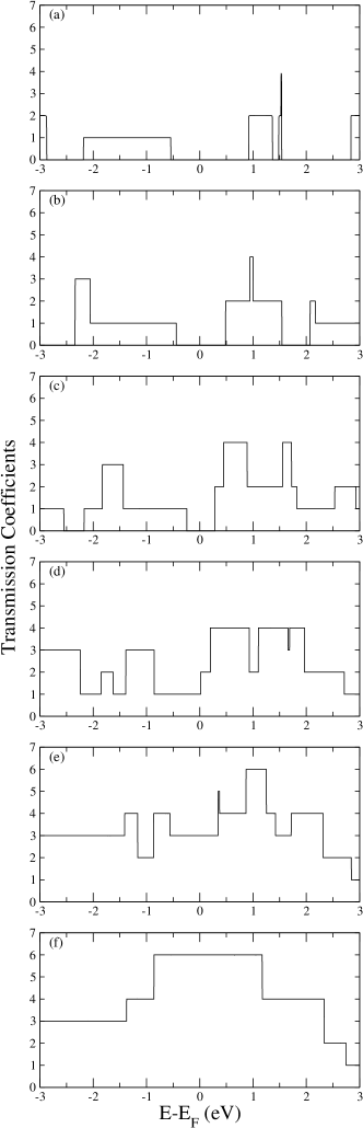
In order to understand the interplay between dimerization and transport, we have calculated the zero-voltage transmission coefficients for six chains with different inter-atomic distances. The unit cell of all chains contains two atoms, and has a lattice constant Å. We have varied the inter-atomic distance of the two atoms in the unit cell from Å (ground state dimer) to Å (equidistant atoms). To characterize all these chains, we introduce the dimer order parameter , which varies from for to for .
We note first that the ground state of all chains is non-magnetic. Figs. (1) (a) to (f) illustrate the evolution of the transmission coefficients with the order parameter. What we find is that as increases from 0.69, many occupied and unoccupied channels move gradually towards the Fermi level, increasing the conductive nature of the chains. There is an insulator-metal transition at about (Fig (1) (d)) and for larger order parameters the chains become metallic. In other words, the insulating character is retained for dimerized chains, where the dimer is strained []. Conversely, not only perfect (), but also slightly dimerized chains [] are metallic. Notice also that the width of the electronic bands and the plateaus of increases with , indicating that the electronic states become more delocalized. The actual conductance increases step-wise from at to at .
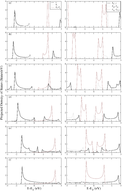
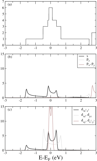
To understand how each state participates in the conductance, we plot the evolution of the projected density of states for each s-, p- and d-orbital in Fig. (2). Notice the chains are oriented along the -axis, which is also the transport direction in our simulations. The d orbitals have therefore the largest hybridizations (that is to say, Hamiltonian matrix elements) among all d-orbitals, followed by the dzx and dzy orbitals (which are equivalent by symmetry), leaving the d and dxy as the less hybridized orbitals. As a consequence, the d orbital feels more strongly the dimerization of the chain, while those states related to the d and dxy orbitals are the least affected. The most relevant effect of the dimerization is the opening of a gap between the bonding and antibonding states, which is largest for the d orbital (6 eV for ) and smallest for the d and dxy orbitals (3.5 eV for ), while the gap is of 5 eV for the states originated from the dxz and dyz orbitals. There is also a hybridized spz orbital below the Fermi level, and a px and py contribution hybridized with the dxz and dyz orbitals. When the order parameter approaches 1, the first channel which reaches the Fermi level and participates in the zero-bias conductance is the spz, followed immediately by the dxz and dyz. In contrast, the gap belonging to the d orbital only closes when , and therefore only contributes to the zero-bias conductance when the atoms in the chain are almost equidistant. When the chain is completely equidistant the gaps in the densities of states disappear and all the d-orbitals contribute to the conductance. Thus, the 6 channels of conductance at the Fermi level for the equidistant chain comes from the 5 d-orbitals and from the spz-orbital, since the contribution of the px and py in the d-orbitals is negligible.
IV One-dimensional Mo electrodes separated by a dimerized region
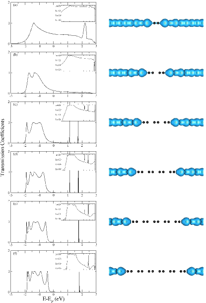
In order to investigate the role of dimers in the scattering region between two conductive electrodes we have considered the formation of 1 to 6 dimers within an infinite equidistant wire. Thus, at both sides of the scattering region we have ideal conductive 1D electrodes. The question that arises is if the current flow is disrupted and how by the dimers. The scattering region, which we call the extended molecule, includes also part of the electrodes (four atoms at each side) to ensure the continuity of the potential with that of the infinite electrodes. To determine the curve we need to evaluate the charge density by using the lesser Green’s function (instead of the retarded one, since electrodes at different potential establish a nonequilibrium population in the extended molecule) and the self-energies of the electrodes at different potentials for all the energy range in the bias window (not only at ). The intensity of the current at a given bias is obtained by using Eq. (1), where
| (5) |
is the retarded Green’s function of the extended molecule, with and the retarded self-energy of the left (right) electrode, and is the Gamma matrix, which gives the strength of the coupling between the scattering region and the left (right) electrode.
We plot in Fig. (3) the zero-voltage transmission for different scattering regions with an increasing number of dimers, from 1 to 6. Each panel has attached to the right a real-space plot of the density of states integrated in a window of 0.5 eV about the Fermi energy. We find that, even if we introduce only one dimer, the transmission at the Fermi level falls from 6 to only 1 G0, due to the lack of transmission channels in the scattering region. For only one dimer we find that some electronic density spreads around the dimer, but becomes rapidly localized when we increase the number of dimers. This indicates again that the transport must be in the tunneling regime, where the low bias conductance decreases exponentially as a function of the distance between electrodes, since electrons at the Fermi energy can only hop from dimer to dimer via tunneling events. The transmission begins to resemble that obtained in the case of the infinite dimerized wire (Fig. (1), top panel) when the number of dimers increases.
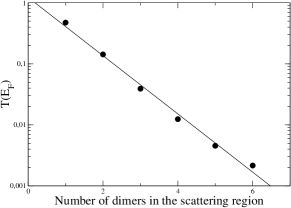
To confirm the tunneling behavior of the conductance, we plot in Fig. (4) the logarithm of the zero-voltage transmission at the Fermi level in a logarithmic scale as a function of the number of dimers in the scattering region. The points are indeed fitted by a linear function, so the transmission coefficients fit to an exponential. To find out the effective height of the tunneling barrier, we set
| (6) |
where Å is the dimer length, is the electron mass and is the number of dimers in the chain. Notice that neither nor are properly defined separately. Rather, only their product can be extracted from the fitting. We pick a common practice when fitting conductance curves in vaccum tunneling, and select to be the physical mass of the electron, thus dumping all the non-trivial renormalizations into the effective height of the barrier. We find that eV, which agrees reasonably well with the gap in the DOS of an infinite dimerized chain.
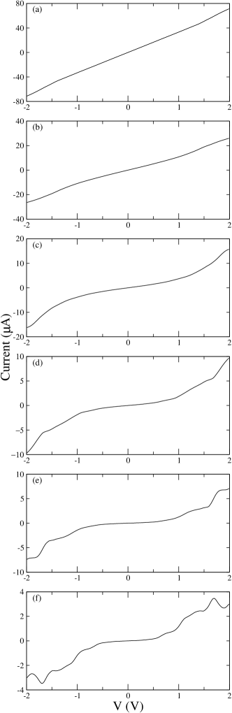
In Fig. (5) we plot the characteristics in a voltage range between -2 and +2 volts, for the different scattering regions mentioned above. We note that the curves look like featureless Ohmic curves when the scattering region comprises just one or two dimers. For a larger number of dimers the curves start to develop a gap of about 2 volts, and a number of additional high-voltage shoulders. These evolve into negative differential resistance (NDR) characteristics for large numbers of dimers. The NDR is produced by a small peak in the transmission coefficients , which is located around -0.75 eV. This peak appears for high absolute values of , but its height has a sudden drop when the is increased beyond 1.7 volts. The drop leads to a concomitant decreases in the electrical current. We find that if is increased even further, a second peak enters inside the integration window when volts, so that the electrical current increases again. The emergence and evanescence of transmission peaks can be understood in terms of the disorder introduced by the bias-dependent on-site energies,Muj96 . We have found a similar NDR effect in thiol-capped polyynes junctions. Garciasu
V Stretched monoatomic Mo wires
The interatomic distances recently measured between Mo atoms in individual monoatomic chains encapsulated inside carbon nanotubesmuramatsu ranged from 3.2 Å to 3.8 Å. Those wires are then far from being dimerized; rather, they are stretched, since those distances are much longer than 2.3 Å, which corresponds to equidistant free-standing chains.
We expect that isolated chains with such long become ferromagnetic because of the Stoner criterion: they must have narrower bands and, as a consequence, a high density of states at the Fermi level in the non-magnetic state. Indeed, we have found that the ground state configuration is characterized by a full spin polarization, where the magnetic moment is saturated to its maximum possible value of 6 per atom, and by a large exchange splitting of xx eV. Hence, all 5d as well as the 6s orbital are completely spin polarized. This ferromagnetic ground state is more stable than the paramagnetic state by 2.3 eV.
We expect that this spin polarization must have an important impact in the transport behavior. Indeed, Häfner et al. Hafner found in a recent work that atomic contacts of Fe, Co and Ni carry spin polarized currents, where the degree of the spin-polarization of the current depended on the type of transport regime (contact or tunneling. To estimate the extent of this impact, we have calculated the transmission in both the non-magnetic and the magnetic states.
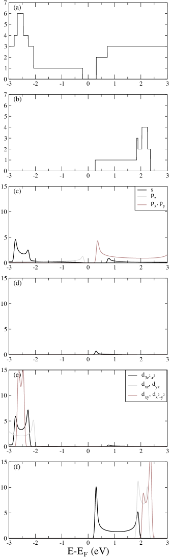
We have computed first the transmission coefficients of an isolated Mo wire in the non-magnetic state with equidistant interatomic distances and a unit cell similar to that found experimentally. The results are shown in Fig. (6). We find that all six s- and d-channels contribute to the transmission coefficient at the Fermi level, like in the equidistant regime discussed in section III. This might look surprising at first glance since the distance between atoms in this stretched chain is even larger than the inter-dimer distance of the dimerized chains with insulating behavior discussed in section III. However, we note that in the equidistant stretched chain the d-orbitals do not form covalent bonds, and since no bonding and antibonding states are formed (with their corresponding gap), the d-electrons are free to participate in the transmission at the Fermi level. Away from the Fermi level, however, the transmission coefficient decreases much faster than in the previous case, since weak bonds due to electron localization generate small bandwidths and, therefore, small energy intervals in the transmission. The narrowing of the bandwidth due to electron localization is clear if we compare the densities of states of Fig. (2) with those corresponding to the equidistant wire in Fig. (6) (lower panel).
We find that the ferromagnetic state is insulating. current is fully spin-polarized for the ferromagnetic state, since all s and d channels with spin down (minority electrons) between -3 and 3 eV contribute to the transmission above to the Fermi level, as can be seen in Fig. (7). We do not observe half-metallic behavior at the Fermi level, however, due to the presence of the large spin splitting which opens to completely occupy the d and s levels with unpaired electrons. The encapsulation inside a nanotube is expected to modify these electronic and transport properties, since there will be a net charge transfer between the chain and the nanotube.
VI Conclusions
We have found that dimerization of molybdenum atomic wires has dramatic effects on their electronic and transport properties. While equidistant wires are metallic and have a very high zero-bias conductance, dimerized wires show a large gap which makes them insulating. As a consequence, the transport properties of dimers between equidistant conducting wires show tunneling behavior. The conductance decreases exponentially as the number of dimers increases in the scattering region and the characteristics start developing a large gap around zero voltages. Other features like plateaus and negative differential resistance also appear for large numbers of dimers.
Equidistant stretched chains are highly conductive in the non-magnetic case. However, the most stable configuration is ferromagnetic, with a very high magnetic moment of 6 per atom.
Acknowledgements.
This work was supported by the Spanish Ministry of Education and Science in conjunction with the European Regional Development Fund (Projects FIS2008-02490/FIS and FIs2006-12117), and by Junta de Castilla y León (Project GR120).References
- (1) A. Nitzan and M. A. Ratner, Science 300, 1384 (2003).
- (2) C. N. Benzryadin, A. Lau, M. Q. Tinkham, Nature 404, 971 (2000).
- (3) M. P. Zach, K. H. Ng, R. M. Penner, Science 290, 2120 (2000).
- (4) N. Nilius, T. M. Wallis, W. Ho, Science 297, 1853 (2002).
- (5) G. Autès, C. Barreteau, D. Spanjaard, and M. C. Desjonquères, Phys. Rev. B 77, 155437 (2008)
- (6) Y. Miura, R. Mazzarello, A. Dal Corso, A. Smogunov, and E. Tosatti, Phys. Rev. B 78, 205412 (2008)
- (7) A. Smogunov, A. dal Corso, R. Weht, A. Delin and E. Tosatti, Nature Nanotech. 3, 22 (2008)
- (8) S. Datta, Electronic Transport in Mesoscopic Systems. Cambridge University Press, Cambridge, UK, 1995.
- (9) A. R. Rocha, V. M. García-Suárez, S. W. Bailey, C. J. Lambert, J. Ferrer and S. Sanvito, Phys. Rev. B73, 085414 (2006).
- (10) A. R. Rocha, V. M. García-Suárez, S. W. Bailey, C. J. Lambert, J. Ferrer and S. Sanvito, Nature Materials 4, 335 (2005).
- (11) W. Kohn and L. J. Sham, Phys. Rev. 140, A1133 (1965).
- (12) J. M. Soler, E. Artacho, J. D. Gale, A. García, J. Junquera, P. Ordejón, and D. Sánchez-Portal, J. Phys.: Condens. Matter 14, 2745 (2002).
- (13) H. Muramatsu, T. Hayashi, Y. A. Kim, D. Shimamoto, M. Endo, M. Terrones, and M.S. Dresselhaus, Nanoletters, http://dx.doi.org/10.1021/nl0725188.
- (14) F. Aguilera-Granja, A. Vega, L. J. Gallego, Nanotechnology 19, 145704 (2008).
- (15) R.H.M. Smit, et al., Phys. Rev. Lett. 91, 076805 (2003).
- (16) L. Fernández-Seivane et al., Phys. Rev. B 75, 075415 (2007)).
- (17) Su et al., Phys. Rev. B 22, 2099 (1980).
- (18) N. Troullier and J. L. Martins, Phys. Rev. B 43, 1993 (1991).
- (19) L. Kleinman and D. M. Bylander, Phys. Rev. Lett. 48, 1425 (1982).
- (20) J. P. Perdew, K. Burke, and M. Ernzerhof, Phys. Rev. Lett. 77, 3865 (1996).
- (21) W. H. Press, S. A. Teukolsky, W. T. Vetterling, and B. P. Flannery,Numerical Recipes in Fortran, 2nd ed. (Cambridge University Press, Cambridge, 1992).
- (22) V. Mujica, M. Kemp, A. Roitberg, and M. Ratner, J. Chem. Phys. 104, 7296 (1996).
- (23) V. M. García-Suárez and C. J. Lambert, Nanotechnology 19, 455203 (2008).
- (24) M. Häfner, J.K. Viljas, D. Frustaglia, F. Pauly, M. Dreher, P. Nielaba, and J.C. Cuevas, Phys. Rev. B 77, 104409 (2008).