Pure, and -doped Graphene nanoflakes: a numerical study of density of states
Abstract
We built graphene nanoflakes doped or not with atoms in the hybridization or with atoms. These nanoflakes are isolated, i.e. are not connected to any object (substrate or junction). We used a modified tight binding method to compute the and density of states. The nanoflakes are semiconducting (due to the armchair geometry of their boundaries) when their are pure but the become conducting when doped because doping removes the degeneracy of the density of states levels. Moreover, we showed that the Fermi level and the Fermi level of both and electrons are not superimposed for small isolated nanoflakes.
pacs:
73.22.Pr;31.15.bu; 31.15.aeI Introduction
The electronic structure of nanoscale graphene has been the subject of intensive research during the last years because of fundamental scientific interest in nanomaterials. With the developments in preparation and synthesis techniques carbon-based nanostructures have emerged as one of the most promising materials for non silicon electronics.
Graphene nanoflakes are either semiconductors or conductors aiming to the geometry of their boundaries heiskanen . Several studies have been published on graphene nanoflakes doped with impurities Pershoguba ; Fogler ; Pellegrino . We decided here to compute the and electrons density of states of graphene nanoflakes doped with a small percentage of either atoms or with hybridized atoms.
We show here numerical results on the conductivity of graphene nanoflakes and on the density of states (mainly the Fermi level) of impurities-doped graphene nanoflakes.
Our numerical method allows us to take into account the as well as the for the calculation of the electronic density of states. And moreover, this method allows one to separate the and the density of states.
II Tight-binding model with hybridization
Let us remind that this is a one electron model, each electron moves in a potential which represents both the nuclei attraction and the repulsion of the other electrons. and electrons are separately treated.
The Hamiltonian of the bonds may be written as:
| (1) |
where the molecular orbital is given by:
| (2) |
with the hybrid orbital () which points from site along the bond ; the energy origin is taken at the vacuum level. and are first neighbours with the average energy: and are the atomic energy levels; is the usual hopping or resonance integral in the tight binding theory (interaction between nearest neighbour atoms along the bond); is a promotion integral (transfer between hybrid orbitals on the same site): .
For an infinite three dimensional crystal (bulk), the gap between valence and conduction band (forbidden band) is (for VIb elements) and may be derived from the values of leleyter .
The Hamiltonian for the bonds is:
| (3) |
with the orbitals centered on atoms and is the hopping integral for levels.
The value for was chosen in order to get the correct positions for energy levels in comparison to the results of the Verhaegen’s ab initio calculations verhaegen .
We need only three parameters:, and for the homonuclear model which represent in fact the average potential and which take into account the nuclear attraction and the dielectronic attraction leleyter . The values of these three parameters are given in table I.
III Results
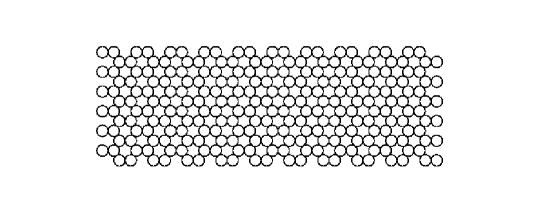
We computed the density of states of pure and doped graphene nanoflakes. The nanoflakes have boundaries represented in figure 1. We studied nanoflakes containing 480, 720 and 960 atoms: we obtained their geometry by reproducing figure 1 in the direction.
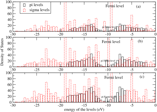
In figure 2, one may see the density of states of nanoflakes of graphene containing 480 atoms. The nanoflakes are isolated, i.e. they are not connected to any other conducting material or connected to any substrate. The 3 graphs in figure 2 representing the DOS (density of states) correspond to: (a) pure graphene nanoflake (b) 5% of Si atoms randomly introduced in the graphene nanoflake and (c) 5% of hybridized carbon atoms randomly distributed within the nanoflake. , 10%, 15% and 20%. The boundaries of the nanoflakes correspond to the armchair geometry.
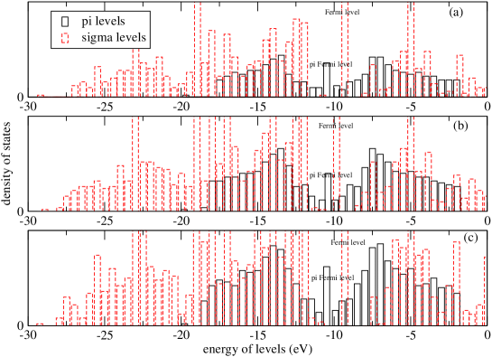
Figure 3 corresponds to the same nanoflakes (i.e. pure, with 5% of atoms and with 5% of hybridized carbon atoms) but in this case for 720 atoms.
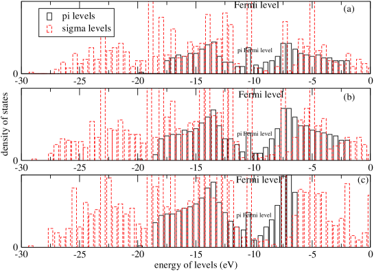
Figure 4 corresponds also to 3 DOS with the same nanoflakes but this time containing 960 atoms.
It is possible to introduce impurities like atoms. Carbon and Silicon belong to the same column IVb of the periodic table. However, their structures in the solid states are different. Carbon indeed can be found in several allotropic varieties such as diamond, graphite, graphene whereas silicon is always found in three dimensional systems.
In mixed silicon-carbon nanoclusters, it has been previously pointed out that experimental results show a progressive transition from a carbon type behaviour of Si to a silicon type behaviour dornenburg as the silicon richness is growing in the clusters leleyter6 . This may be transferred in nanoflakes to the percentage of : here we deal with small percentages of surrounded by 95% of at least. From references dornenburg ; leleyter6 we may say that due to the richness in carbon atoms in the studied nanoflakes of graphene, the atoms adopt the carbon behaviour i.e. are in the hybridization.
IV Discussion
It is worth noticing that for small and finite size nanoflakes, the DOS consists of many discrete levels and instead of Fermi level, one should speak of highest occupied molecular orbital (HOMO) and lowest unoccupied molecular orbital (LUMO).
However, we retain these terms in a loose sense because the main result when comparing the three figures of DOS for the nanoflakes of graphene of different sizes, we observe (figures 2,3 and 4) that the Fermi (or HOMO) level of the electrons DOS correspond to the DOS in the direction in the Brillouin zone (see for that reference wakabayashi . The fact is that for 480 atoms and 720 atoms of pure graphene (figures 2(a) and 3(a)) the DOS shows that there is a gap between the Fermi level and higher energy levels: this indicates that the nanoflake of pure atoms is semiconducting. This is in good agreement with the literature showing that with armchair boundaries (which is the case in our nanoflakes) semiconducting is generally obtained heiskanen .
By doping the nanoflake with either atoms or by carbon atoms, one destroys the semiconducting character. This is due to the fact that impurities remove the degeneracy of the energy levels.
What is also interesting is that the Fermi level and the whole Fermi level are not superimposed for nanoflakes containing a small number of atoms (480 and 720 atoms: fig. 2 and 3). The superimposition only occurs for a larger number of atoms (here 960 atoms: fig.4). Generally in the literature, one studies the DOS as the major numerical methods used by authors is the tight binding one taking only account of electrons. But here, we deal with and atoms, and when calculating the Fermi the and the whole Fermi level, these two do not superimpose, at least for a small number of atoms. But electrons do not enter in the conducting or semiconducting character of the sample.
V Conclusion
Let us summarize the results: doping graphene nanoflakes with armchair boundaries removes the degeneracy of the energy levels in the DOS and therefore removes the semiconducting character of graphene nanoflakes with this kind of boundaries; the Fermi level and joint and Fermi level do not superimpose for small graphene nanoflakes: but as the electrons do not enter conduction this has no consequence on the electronic features of small graphene nanoflakes.
References
- (1) H.P.Heiskanen, M.Manninen and J.Akola, New J. of Phys. 10 (2008) 103015
- (2) S.S.Pershoguba,V.Y.Skrypnyk, V.M.Loktev, Phys. Rev. B 80 (2009) 214201 and references within
- (3) M.M.Fogler,Phys. Rev. Lett. 103 (2009) 236801 and references within
- (4) F.M.D. Pellegrino,G.G.N. Angilella,R.Pucci, Phys. Rev. B 80 (2009)094203 and references within
- (5) M.Leleyter and P.Joyes, J.Phys. 36 (1975) 343
- (6) G.Verhaegen, J.Chem.Phys. 49 (1968) 4696
- (7) E.Dornenburg,H.Hintenberger, Z.Naturforsch. 14a (1959) 765
- (8) M.Leleyter, J.Microsc.Spectrosc.Electron. 7 (1989) 61
- (9) K.Wakabayashi, M.Fujita, H.Ajiki and M.Sigrist, Phys. Rev. B 59 (1999) 8271
| atom/parameter | ||||
|---|---|---|---|---|
| 19.45 | 10.74 | 7.03 | 3.07 | |
| 14.96 | 7.75 | 4.17 | 0.8 |