Resonant tunnelling features in the transport spectroscopy of quantum dots
Abstract
We present a review of features due to resonant tunnelling in transport spectroscopy experiments on quantum dots and single donors. The review covers features attributable to intrinsic properties of the dot as well as extrinsic effects, with a focus on the most common operating conditions. We describe several phenomena that can lead to apparently identical signatures in a bias spectroscopy measurement, with the aim of providing experimental methods to distinguish between their different physical origins. The correct classification of the resonant tunnelling features is an essential requirement to understand the details of the confining potential or predict the performance of the dot for quantum information processing.
1 Introduction
With the rapid miniaturization of electronic devices comes the need to understand their operation at an unprecedented level. Quantum mechanical effects are becoming increasingly important in the design of nanometre-scale transistors [1], posing new challenges in the experimental characterization and corresponding theoretical description of the devices that will constitute the next generations of commercial electronics. Quantum effects in the electron transport of nanodevices have already been the subject of many years of fundamental research. Single-electron devices [2] are the focus of much of this research, possessing highly non-linear current-voltage characteristics resulting from a combination of quantum mechanical (charge quantization, discrete energy levels) and classical effects (Coulomb repulsion). These properties have lead to single-electron devices being used as ultra-sensitive charge sensors [3] and amplifiers for quantum signals [4]. Here the term “single-electron device” refers to the fact that the current consists of individual electrons, sequentially flowing through a nanostructure.
Upon further miniaturization, one reaches the fully quantum-mechanical regime of few-electron quantum dots [5] or single-donor devices [6, 7, 8, 9]. Both types of quantum wells are characterized by an electron confinement strong enough to create single-particle energy levels with a spacing larger than the thermal broadening. This allows individual resolution of the energy levels of the quantum dot, whether from electrostatically defined dots or arising from a donor potential. In this work we will refer to both types of devices as ‘(quantum) dots’, unless specifically mentioned otherwise. Few-electron quantum dots are the subject of intense investigation in the context of quantum information processing [10]. Individual charge carriers confined in quantum dot structures can be used to encode quantum information using either the charge [11, 12, 13, 14, 15] or the spin [16, 17, 18, 19, 20, 21, 22, 23, 24, 25] degree of freedom. For this purpose it is essential that the electrons occupy well-defined energy states, and the details of the excitation spectrum are vital in determining, for instance, the coherence and relaxation times of the qubit [26, 27, 28].
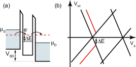
The most common experimental method to investigate the energy level structure of a dot is bias spectroscopy [29, 30]. For a dot coupled to source and drain reservoirs, resonant tunnelling occurs when occupied electronic states in the source and/or drain align with available states in the dot, as sketched in Figure 1(a). This allows electrons to flow sequentially through the dot and to be detected as a change in source-drain current. Voltages on nearby gates are used to control the electrochemical potential of the dot. A bias spectroscopy experiment is a measurement of the source-drain conductance as a function of source-drain bias and gate voltages. This yields a 2-dimensional map as shown in Figure 1(b), which contains diamond-shaped regions with well-defined charge number on the dot (Coulomb diamonds). Resonant tunnelling features induce a distinct change in current above normal device fluctuations and appear as lines running parallel to the diamond edges. Such features are commonly observed in single-electron devices, however their explanation is often simplistic or lacking. This is a result of there being many possible sources of resonant tunnelling features, only identifiable via subtle differences in their behaviour.
In this article we give an overview of the different resonant tunnelling features expected in bias spectroscopy experiments of single-dot devices. The discussion is restricted to the most common operating conditions, corresponding to sequential single electron tunnelling. We review methods for determining the nature of these features with reference to experimental examples, and aim at providing clear guidelines to distinguish between features of different physical origin. We only consider shifts or extensions of the lines, without discussing their width or shape. These methods will serve as a resource for the engineer or physicist seeking to explain measurement results or design next generation single-electron devices.
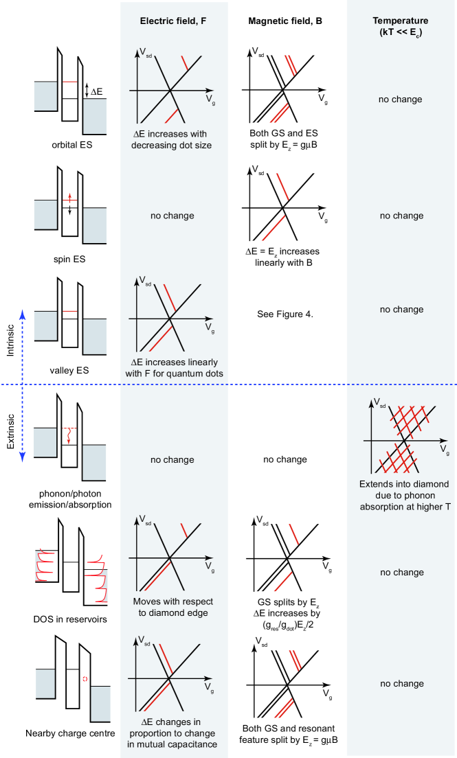
The paper is structured around Figure 2, which summarizes the different conditions that lead to resonant tunnelling features in bias spectroscopy, as well as methods to identify them. The main distinction we draw is between “intrinsic features”, originating from the internal energy level structure of the dot, and “extrinsic features”, appearing because of discrete levels or quantized modes in the environment coupled to the dot.
2 Intrinsic features
2.1 Orbital excited states
Electrons are added to a dot when their potential is raised enough to overcome the addition energy, the sum of the energy level spacing and the Coulomb repulsion from electrons already on the dot [31]. Detecting and mapping the addition of electrons is precisely the purpose of a bias spectroscopy experiment, as explained in the previous section. Excited states of the dot that enter the bias window will increase the current due to the introduction of an additional conductance channel. These states will ideally appear as steps in the current, running parallel to the Coulomb diamond edge. The change in current will not always be step-like, since changing the source-drain bias or gate voltage affects to some degree the tunnel barriers, the confining potential and the coupling to reservoir states. Step-like behaviour will be visible in only one biasing direction if the device contains asymmetric tunnel barriers [32, 33].
The excited state spectrum of a dot is a function of the material and operating conditions (e.g. confinement strength and effective mass), with energy level separation varying from the order of eV for large quantum dots [34] up to 100 meV in ultrasmall dots [35]. In some simple cases, the particle-in-a-box approximation [29] can be used to calculate the orbital level spacing. This simplification must however be applied with caution, since it often produces a value that seems consistent with experimental observations but could be explained equally well by other phenomena.
Varying the size of the dot helps identify resonant tunnelling features as being due to orbital excited states. Changing the dot size will change its excited state spectrum. If the dot size is defined electrostatically, for example through depleting a buried charge layer, then changing the dot size is generally possible by varying the nearby gate potentials.
In a simple rate equation model of sequential tunnelling through a dot [36], the current across the left barrier for positive source-drain bias is given by,
| (1) | |||||
| (2) |
where is the tunnel rate from the dot ground state (g) through the right barrier (r), and similarly for the excited state (e) and left barrier (l). represents the probability of occupying the excited (ground) state and is its degeneracy. If we assume that the tunnel rate into the ground state is approximately equal to that for the excited state, then equation (2) simplifies to
| (3) |
Similarly the current under negative bias is given by
| (4) |
Equations (3) and (4) show that in the presence of asymmetric tunnel barriers (e.g. ), the magnitude of the current step due to the addition of an excited state to the bias window will be different for positive and negative source-drain bias. Conversely, if the tunnel rate into the excited state is much higher than into the ground state (), then asymmetric barriers will result in both positive and negative bias currents and being dominated by the tunnel rate into the excited state through the rate limiting barrier (i.e. if , then ).
Higher order tunnelling events through dot states can provide further information on the source of resonant tunnelling features [37]. Tunnelling processes simultaneously involving two or more electrons (known as co-tunnelling) appear in bias spectroscopy as lines traversing Coulomb diamonds where transport is normally blocked. When co-tunnelling lines join resonant tunnelling features in adjacent diamonds, those features must be due to an intrinsic property of the dot. Co-tunnelling has been clearly observed, for example, in a vertical few-electron InGaAs quantum dot [38] as well as in lateral GaAs [39] quantum dots.
The first experimental example of analysis of orbital excited states of a quantum dot via bias spectroscopy was in 1992 [40]. Here, gate voltage sweeps performed at different source-drain biases showed signatures of 0D dot states, identified by their correspondence with the calculated energy level spacing. A similar study was completed soon after, generating the first full ‘stability diagram’ of conductance in the bias vs gate-voltage plane [41].
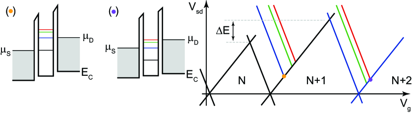
The excitation spectra and sizes of adjacent Coulomb diamonds can provide additional evidence for orbital excited states. As mentioned previously, the addition energy, i.e. the energy required to add one electron to a dot, is equal to , where is the charging energy and the orbital energy. The addition energies of two consecutive electrons entering the same orbital are equal to and . The Coulomb diamond heights of the and diamond should thus differ by the orbital energy, assuming a constant charging energy. If higher orbital excited states appear, then the spectra of the and diamond should be the same except for the energy shift, as shown in Figure 3. This effect has been observed very clearly, for example, in carbon nanotubes [42] as well as GaAs heterostructures [43] and Au nanoparticles [44].
2.2 Spin excited states
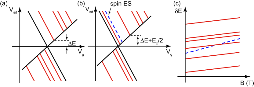
The behaviour of discrete quantum states in response to static magnetic fields is well understood [30]. A magnetic field breaks the spin degeneracy of the ground and excited states. The resulting split states will be separated by the Zeeman enery , where is the electronic g-factor, is the Bohr magneton and is the magnitude of the applied magnetic field. For positive g-factor materials such as silicon, the spin-down level becomes the ground state and spin-up the excited state, separated by the Zeeman energy . The net result is that the spin excited state moves at a rate with respect to the Coulomb diamond edge, as shown in Figure 2.
A clear example of spin excited states has been reported in [45]. The observed resonant tunnelling features correspond to spin-split orbital excited states of a single-electron GaAs quantum dot. Both the ground state and the orbital excited state are spin-degenerate at 0 T, and split by the Zeeman energy as a magnetic field is applied. Over the range from 6 T to 10 T the splitting of both ground and orbital states increases by roughly the same amount.
Spin excited states have been studied comprehensively in GaAs dots [30, 46, 47, 48]. Detailed measurements at different magnetic fields show how the excited state moves with respect to magnetic field according to . Spin excited states of single dots have also been measured in metal nanoparticles [49], carbon nanotubes [42, 50], InAs nanowires [51], Si nanowires [52], Si/Ge nanowires [53] and donors in silicon [9, 54].
2.3 Valley excited states
In some materials degeneracies exist in the carrier band, such as the six-fold conduction band degeneracy in bulk silicon [55]. Restricting the momentum of electrons in a silicon device by applying confining potentials or strain in specific directions can lift this degeneracy [56, 57, 58]. The energy separation of the conduction band minima (valleys) then causes additional features in a transport spectroscopy measurement, i.e. valley excited states. In quantum dots, breaking all valley degeneracies results in a complicated order of filling of electron states based on the relative size of the orbital level spacing, interaction energies, Zeeman energy and valley splitting. In addition, the valley-orbit interaction can lead to a mixing of the orbital wave functions, such that orbitals and valleys are no longer good quantum numbers [59]. The situation is usually simpler in donor confinement potentials, where the orbital level spacings are very large. For clarity, in the discussion below we shall assume the existence of distinct orbital and valley quantum numbers.
For degenerate multi-valley dots, electrons are added to the same orbital in each of the valleys (Figure 4(a)). Valley excited states will be preferentially populated if the valley degeneracy is broken and the exchange and orbital energies are greater than the valley splitting, as in the sketch in Figure 4(c). This is due to exchange interaction being negligible for electrons populating different valleys [60]. Here electrons are added to two different valleys consecutively, resulting in a total spin S=1 for the N=2 state. This is in contrast to the S=0 state that would result in a single valley dot, where the N=2 ground state is a singlet (provided the orbital level spacing is larger than the exchange energy [43, 61]). The magnetic field dependence of the zero bias Coulomb peaks can therefore be used to help identify the origin of resonant tunnelling features. As shown in Figure 4(d), the electrochemical potential will not change with increasing magnetic field when parallel spins are consecutively added to a dot (here N=12). Adding an electron of opposite spin to the same orbital will however induce an increase in electrochemical potential with increasing magnetic field. The spin filling of consecutive electrons follows from the evolution of the Coulomb peak spacing in ground state magnetospectroscopy [62]. This experimental method thus helps to recognize whether the electrons fill different orbitals or different valleys [63].
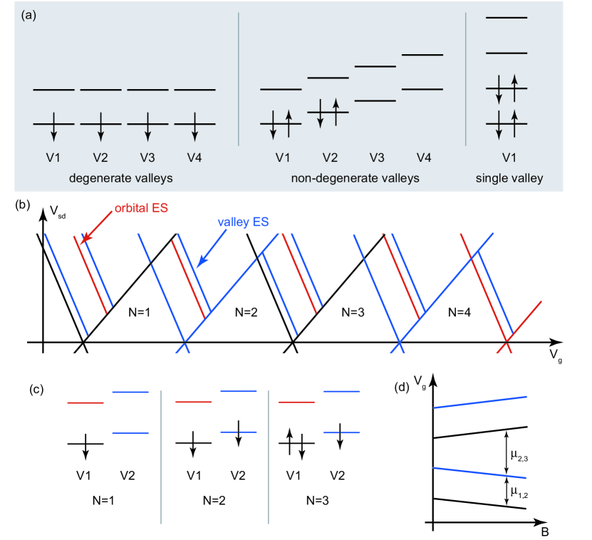
For a two-dimensional electron gas (2DEG) created in the [001] plane in silicon, the confinement will be in the same direction as the longitudinal effective mass for two of the six valleys. These two z-valleys are therefore lower in energy than the four remaining valleys. The degeneracy of the z-valleys may be broken for a tightly-confined 2DEG, depending on the properties of the nearby interface [57, 59, 64, 65]. This splitting can be as high as a few meV for strong electric fields and enhanced by applying additional degrees of confinement [66, 67]. For common operating conditions, the z-valley splitting is linear in the applied field [68, 69].
Valley excited states are also shifted via an electric field due to the Stark effect. For donors in silicon, electric fields exceeding 2-3 MV/m will lead to appreciable Stark shifting [70, 71]. If the donor is near an interface, an accumulating electric field can lead to the hybridization of the donor wavefunctions with those of interface confined states [72, 73], leading to vastly different excited states from those observed in the bulk.
Splitting of the lowest two kz valleys in a silicon inversion layer was first observed in 1966 [74]. Subsequent experimental work in resonant tunnelling through quantum wells has also led to observation of valley splitting in Si/Ge [75, 76, 77] and SiO2/Si/SiO2 devices [64]. A comprehensive study of valley splitting in silicon dots is lacking, although level filling of an SOI quantum dot has been reported [78]. Here, the evolution of Coulomb peaks with magnetic field reveals a filling of the first five charges with alternating spin-down and spin-up electrons, implying non-degenerate valleys as in the middle panel of Figure 4(a).
3 Extrinsic features
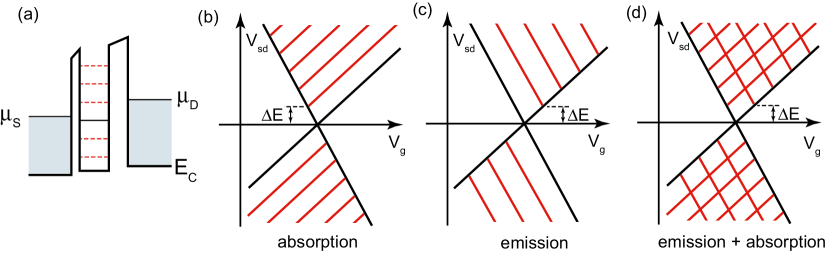
3.1 Photon/phonon assisted tunnelling
Photon and phonon emission and absorption are capable of enhancing current through a dot by offering additional inelastic tunnelling processes. A resonant tunnelling current upon emission of photons or phonons relies on charge carriers tunnelling into or out of the dot by an inelastic relaxation process. In the case of very low temperatures, the number of populated phonon modes vanishes, preventing the absorption of energy from the phonon bath. Upon increasing the temperature, phonon modes become occupied and phonon absorption allows current to flow through the dot when it would be otherwise blockaded at . Photonic/phononic excitations are most easily identified as being independent of magnetic field.
If the process of relaxation or excitation possesses a discrete energy spectrum that becomes resonant with a tunnelling event, additional features will be observed in bias spectroscopy, see Figure 5. For the case when a well-defined cavity exists within a device, a discrete phonon energy spectrum will be present and allow enhanced electron tunnelling through emission at discrete energies. The spacing of resonant tunnelling features due to phonon emission is given by
| (5) |
where and are respectively the speed and wavelength of the photon/phonon. In the case of a closed (open) cavity the wavelength is equal to 2 (4), where is the length of the photon/phonon cavity that the tunnelling electrons are coupled to. The corresponding wavelengths thus follow from the energies at which the resonances are observed.
In case of phonon emission, many roughly equidistant resonant tunnelling features appear at energies . An energy emission of can be described by two possible scenarios: (i) one phonon with energy is emitted. Each line corresponds to one phonon mode of energy , hence the modes are equidistant in energy as in a harmonic oscillator potential. Such a regular set of phonon modes may well have similar shapes, resulting in comparable electron-phonon couplings and current peak heights for all modes. (ii) phonons with energy are emitted. The latter process requires a very strong electron-phonon coupling [79].
For symmetric tunnel barriers, resonant tunnelling features due solely to emission to a discrete phonon spectrum run parallel to both Coulomb diamond edges. In the presence of asymmetric tunnel barriers, lines will be visible in only one direction for absorption (Figure 5(b)) and emission (Figure 5(c)). If both phonon emission and absorption are present, lines will appear in both directions as shown in Figure 5(d).
Raising the temperature to stimulate phonon absorption will give a conclusive answer as to whether phonon-assisted tunnelling is the source of resonant features. Conductance peaks in carbon nanotube quantum dots extend into the Coulomb blockaded regions upon increasing the device temperature [80]. Phonon-assisted tunnelling has also been shown to increase the conductance both by spontaneous emission, e.g. [81, 82, 83] and absorption, e.g. [84]. In the latter experiment the absorbed phonons were on-chip generated surface acoustic waves. Another experimental example is the observation of phononic excitations in Si nanowires [52]. Here, the absence of the magnetic field dependence of the resonant tunnelling features provides strong evidence that their origin was phonon emission. Others have explored features in transport spectroscopy of suspended GaAs quantum dots where low-bias current is suppressed [85]. The ‘phonon blockade’ is due to the formation of a ‘dressed’ dot-phonon state resulting from strong electron-phonon coupling. Bias spectroscopy of single molecule transistors has also allowed the observation of excited states due to vibrational modes of the molecule [86, 87]. Detailed numerical calculations were able to confirm that the energies of certain molecular vibrational modes matched the observed feature spacing. Similarly, an excitation spectrum of suspended carbon nanotubes was found to be consistent with calculation of its vibrational modes, and an order of magnitude smaller than the dot orbital levels [88].
In a manner analogous to phonon absorption, electromagnetic radiation (i.e. photons) causes a peak in current when an applied field becomes resonant with an otherwise prohibited tunnelling event, see [89] and references therein. This photon-assisted tunnelling (PAT) appears in a bias spectroscopy measurement as an extension of the orbital excited state line into the Coulomb diamond, resulting in a similar stability diagram to that shown for phonon absorption in Figure 2. Observation of PAT through excited dot states is in fact usually achieved at a single (often zero) bias [90, 91, 92]. The results in [90] demonstrate PAT in a GaAs quantum dot, observing a dot orbital excited state at zero bias in addition to satellite peaks caused by absorption of the microwave photons. A more recent experimental example of PAT through single dots is the pumping of electrons through excited dot states in carbon nanotubes via application of a high frequency field [91]. The frequency independence of certain resonant tunnelling features whilst the device was under irradiation was identified as a signature they were in fact due to excited states of the dot and not due to the reservoirs. Photon-assisted resonant tunnelling through a device consisting of a single donor coupled to source and drain leads has also been demonstrated [92]. Excited states of the donor were observed at zero bias by irradiating the device with a 40 GHz AC signal. Earlier work focused on the additional features introduced by photon absorption in a large quantum dot, but was not used to probe the dot’s excited states [93, 94].
3.2 DOS of the reservoirs
As discussed earlier, bias spectroscopy requires a source and drain of charge carriers in order to probe the states of the dot. The properties of these reservoirs will strongly influence the behaviour of the device, and in some cases be themselves the origin of resonant tunnelling features. The DOS of the reservoirs within the bias window determines the availability of charge carriers for tunnelling, hence singularities in the reservoir DOS will appear in the bias spectroscopy.
For the case where the source and drain reservoirs are electrostatically induced two-dimensional charge layers, e.g. from modulation doped heterostructures or gate induced inversion/accumulation layers, the confinement perpendicular to the 2DEG plane quantizes the -momentum of the carriers into distinct subbands. Discontinuous changes in the 2D DOS occur when a different subband becomes occupied. Only the lowest subband is occupied for high confining fields or low temperatures [95]. The DOS in this 2DEG subband is independent of energy (i.e. constant) [55], and therefore the reservoirs do not contribute any sharp transport feature. However, if the width of the reservoirs becomes comparable to the mean free path, , quasi-1D DOS features arise. We use the term ‘quasi-1D’ since, if many 1D subbands are occupied, a 2D DOS is recovered. The elastic mean free path is proportional to the mobility, of the 2DEG through,
| (6) |
where is the Fermi velocity, is the Fermi wave vector, is the effective mass and is the elastic scattering time. Typical values for the mean free path are in the range nm in silicon and m in GaAs 2DEGs. For reservoirs with width comparable to or less than , the number of states per subband is given by,
| (7) |
where is the subband energy. Equation (7) shows that a singularity in the DOS is reached at energies equal to any of the subbands. Experimentally, these DOS peaks will be asymmetric, rising sharply then falling proportional to , where is the Fermi energy. However scattering off lattice, impurity and interface defects often broadens these peaks and make it difficult to observe their rolloff.
The spacing of the subband energy levels can be approximated in a number of ways. For an electron accumulation/inversion layer, the subbands due to motion perpendicular to the interface are well approximated by the eigenvalues of a triangular well [96],
| (8) |
Here is the conduction band minimum, is the confining electric field and is the subband index. In silicon, the longitudinal effective mass applies to electrons populating the kz-valleys and the transverse effective mass to electrons in the kx- and ky- valleys. By changing the magnitude of the confining field two effects take place: 1) the increase in confinement strength changes the subband energies; and 2) the conduction/valence band edge moves relative to the Fermi level. The latter effect will dominate, since changing the field scales the indexed subbands by and has little effect on the width of the inversion layer. Therefore, directly gating the reservoirs helps identifying resonant tunnelling features originating from the source or drain DOS, since they will move relative to the Coulomb diamond edge. This is summarized schematically in Figure 2 and has recently been demonstrated experimentally [97]. With asymmetric tunnel barriers, only resonant tunnelling features relevant to the rate limiting barrier will be observed, leading to features running in only one direction in a bias spectroscopy measurement.
In a magnetic field, the DOS of the reservoirs and the energy spectrum of the dot split by the Zeeman energy. The splitting will be equal if both reservoir and dot possess the same -factor, meaning features in the transport spectroscopy measurement due to the reservoirs will not split. This is in contrast to spin excited states of the dot itself, see Figure 6(a) and (b). Furthermore, the lower energy spin states of the dot (including the Coulomb diamond edge) will shift down in voltage by Ez/2 while the DOS features will not move. Plotting the shift of all the features relative to the Coulomb diamond edge will show dot states splitting and/or moving by Ez whereas features originating from the reservoir will move by Ez/2, as shown in Figure 6(c).
Transport spectroscopy features have been attributed to structure in the DOS for many years, for example the quasi-1D features observed in narrow MOSFET channels [98, 99, 100, 101] and carbon nanotubes [102, 103, 104]. The influence of the reservoir DOS was first seen in the pioneering work on discrete energy levels in metal nanoparticles [49]. Here, the BCS DOS of the superconducting leads were visible as peaks in the tunnelling current through a single Al particle. The first experimental observations of features in resonant tunnelling through semiconductor quantum dots attributable to peaks in the reservoir DOS were achieved in 1997 [105, 106]. At a later stage others have made similar observations [33, 39, 73, 107], although a study of these features was not the primary objective of their work.
Fluctuations in the local DOS of disordered reservoirs attributed to interference of diffusive charge carrier wavefunctions also cause features in the transport spectroscopy of quantum dots. Since these features are dominated by disorder, their behaviour in a magnetic field is complicated [108, 109] if not random [110]. They are also independent of devices size and temperature [111].
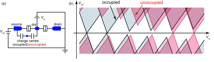
3.3 Nearby charge centres
The change in population of a charge centre located in the tunnel barrier or near the reservoirs can also give rise to resonant tunnelling features in bias spectroscopy measurements [112, 113]. These features are strongly dependent on the capacitive coupling between the charge centre, the dot and the gate, as well as the proximity of the charge centre energy levels to the reservoir Fermi level. For weakly coupled traps, the resonant features will be the same on all Coulomb diamonds [113]. Strongly coupled charge centres however, produce a more obvious signature where the change in charge centre occupancy results in additional diamonds appearing alongside or in between the original diagram, as shown in Figure 7. In a magnetic field, the states of both the dot and the charge centre will split by the Zeeman energy, behaving in the same way as orbital states of the dot. Characterization of the coupling capacitances enables extraction of the location of the charge centre with respect to the gates, and detuning of such charging events. Detailed experimental studies of this type of resonant tunnelling event have been undertaken [112, 113, 114]. We note that the coupling between a dot and a nearby charge centre has also been proposed as a method to read out the spin of the charge centre [25].
4 Conclusions
Resonant tunnelling features in the bias spectroscopy of quantum dots can arise from a broad range of physical phenomena. We have shown that the response of a quantum dot to experimentally accessible parameters, such as electric and magnetic fields or the temperature, can be used to identify the nature of the tunnelling features. This task is important for a variety of reasons, ranging from the basic recognition of the nature of the binding potential due to dopants [73], to the assessment of the feasibility of quantum computing schemes in quantum dots [115]. Therefore, the information obtained from bias spectroscopy experiments can form the first step towards understanding and predicting the properties of quantum dots.
References
References
- [1] Levi A J F. Towards quantum engineering. Proc. of the IEEE, 96(2):335–342, 2007.
- [2] Likharev K K. Single-Electron Devices and Their Applications. Proceedings of the IEEE, 87(4):606–632, 1999.
- [3] Brenning H, Kafanov S, Duty T, Kubatkin S, and Delsing P. An ultrasensitive radio-frequency single-electron transistor working up to 4.2 k. J. Appl. Phys., 100(11):114321, 2006.
- [4] Devoret M H and Schoelkopf R S. Amplifying quantum signals with the single-electron transistor. Nature, 406:1039–1046, 2000.
- [5] Kouwenhoven L P, Austing D G, and Tarucha S. Few-electron quantum dots. Rep. Prog. Phys., 64(6):701–736, 2001.
- [6] Sellier H, Lansbergen G P, Caro J, Rogge S, Collaert N, Ferain I, Jurczak M, and Biesemans S. Transport Spectroscopy of a Single Dopant in a Gated Silicon Nanowire. Phys. Rev. Lett., 97(20):206805, 2006.
- [7] Calvet L E, Wheeler R G, and Reed M A. Observation of the linear Stark effect in a single acceptor in Si. Phys. Rev. Lett., 98(9):96805, 2007.
- [8] Khalafalla M A H, Ono Y, Nishiguchi K, and Fujiwara A. Identification of single and coupled acceptors in silicon nano-field-effect transistors. Appl. Phys. Lett., 91:263513, 2007.
- [9] Tan K Y, Chan K W, Möttönen M, Morello A, Yang C, van Donkelaar J, Alves A, Pirkkalainen J M, Jamieson D N, Clark R G, and Dzurak A S. Transport spectroscopy of single phosphorus donors in a silicon nanoscale transistor. Nano Lett., 10(1):11–15, 2010.
- [10] DiVincenzo D P and Bennett C. Quantum information and computation. Nature, 404(3):247–255, 2000.
- [11] Fedichkin L, Yanchenko M, and Valiev K A. Coherent charge qubits based on gaas quantum dots with a built-in barrier. Nanotechnology, 11(4):387–391, 2000.
- [12] Hayashi T, Fujisawa T, Cheong H D, Jeong Y H, and Hirayama Y. Coherent manipulation of electronic states in a double quantum dot. Phys. Rev. Lett., 91(22):226804, 2003.
- [13] Hollenberg L C L, Dzurak A S, Wellard C, Hamilton A R, Reilly D J, Milburn G J, and Clark R G. Charge-based quantum computing using single donors in semiconductors. Phys. Rev. B., 69(11):113301, 2004.
- [14] Petta J R, Johnson A C, Marcus C M, Hanson M P, and Gossard A C. Manipulation of a single charge in a double quantum dot. Phys. Rev. Lett., 93(18):186802, 2004.
- [15] Gorman J, Hasko D G, and Williams D A. Charge-qubit operation of an isolated double quantum dot. Phys. Rev. Lett., 95(9):090502, 2005.
- [16] Loss D and DiVincenzo D P. Quantum computation with quantum dots. Phys. Rev. A, 57(1):120–126, 1998.
- [17] Kane B E. A silicon-based nuclear spin quantum computer. Nature, 393(6681):133–137, 1998.
- [18] Vrijen R, Yablonovitch E, Wang K, Jiang H W, Balandin A, Roychowdhury V, Mor T, and DiVincenzo D. Electron-spin-resonance transistors for quantum computing in silicon-germanium heterostructures. Phys. Rev. A., 62(1):012306, 2000.
- [19] Friesen M, Rugheimer P, Savage D E, Lagally M G, van der Weide D W, Joynt R, and Eriksson M A. Practical design and simulation of silicon-based quantum-dot qubits. Phys. Rev. B., 67(12):121301(R), 2003.
- [20] Elzerman J M, Hanson R, Willems van Beveren L H, Witkamp B, Vandersypen L M K, and Kouwenhoven L P. Single-shot read-out of an individual electron spin in a quantum dot. Nature, 430:431–435, 2004.
- [21] Petta J R, Johnson A C, Taylor J M, Laird E A, Yacoby A, Lukin M D, Marcus C M, Hanson M P, and Gossard A C. Coherent Manipulation of Coupled Electron Spins in Semiconductor Quantum Dots. Science, 309:2180–2184, 2005.
- [22] Cerletti V, Coish W A, Gywat O, and Loss D. Recipes for spin-based quantum computing. Nanotechnology, 16(4):R27–R49, 2005.
- [23] Hill C D, Hollenberg L C L, Fowler A G, Wellard C J, Greentree A D, and Goan H S. Global control and fast solid-state donor electron spin quantum computing. Phys. Rev. B., 72(4):045350, 2005.
- [24] Tokura Y, van der Wiel W G, Obata T, and Tarucha S. Coherent single electron spin control in a slanting zeeman field. Phys. Rev. Lett., 96(4):047202, 2006.
- [25] Morello A, Escott C C, Huebl H, Willems van Beveren L H, Hollenberg L C L, Jamieson D N, Dzurak A S, and Clark R G. Architecture for high-sensitivity single-shot readout and control of the electron spin of individual donors in silicon. Phys. Rev. B., 80(8):081307(R), 2009.
- [26] Khaetskii A V and Nazarov Y V. Spin relaxation in semiconductor quantum dots. Phys. Rev. B., 61(19):12639–12642, 2000.
- [27] Tahan C and Joynt R. Rashba spin-orbit coupling and spin relaxation in silicon quantum wells. Phys. Rev. B., 71(7):075315, 2005.
- [28] Stano P and Fabian J. Orbital and spin relaxation in single and coupled quantum dots. Phys. Rev. B., 74(4):045320, 2006.
- [29] Sohn L L, Kouwenhoven L P, and Schön G. Mesoscopic Electron Transport. Kluwer Academic, 1997.
- [30] Hanson R, Kouwenhoven L P, Petta J R, Tarucha S, and Vandersypen L M K. Spins in few-electron quantum dots. Rev. Mod. Phys., 79(4):1217–49, 2007.
- [31] Grabert H and Devoret M H. Single charge tunneling: Coulomb blockade phenomena in nanostructures. Plenum Press, New York, 1992.
- [32] Cobden D H, Bockrath M, McEuen P L, Rinzler A G, and Smalley R E. Spin Splitting and Even-Odd Effects in Carbon Nanotubes. Phys. Rev. Lett., 81:681–684, 1998.
- [33] Björk M T, Thelander C, Hansen A E, Jensen L E, Larsson M W, Wallenberg L R, and Samuelson L. Few-Electron Quantum Dots in Nanowires. Nano Lett., 4(9):1621–1625, 2004.
- [34] Beenakker C W J. Theory of coulomb-blockade oscillations in the conductance of a quantum dot. Phys. Rev. B, 44(4):1646, 1991.
- [35] Zwanenburg F A, van Loon A A, Steele G A, van Rijmenam C E W M, Balder T, Fang Y, Lieber C M, and Kouwenhoven L P. Ultrasmall silicon quantum dots. J. Appl. Phys., 105:124314, 2009.
- [36] Bonet E, Deshmukh M M, and Ralph D C. Solving rate equations for electron tunneling via discrete quantum states. Phys. Rev. B., 65(4):045317, 2002.
- [37] Averin D V and Nazarov Y V. Single charge tunneling: Coulomb blockade phenomena in nanostructures, chapter Macropscopic quantm tunneling of charge and co-tunneling. Plenum Press, New York, 1992.
- [38] De Franceschi S, Sasaki S, Elzerman J M, van der Wiel W G, Tarucha S, and Kouwenhoven L P. Electron cotunneling in a semiconductor quantum dot. Phys. Rev. Lett., 86(5):878, 2001.
- [39] Zumbühl D M, Marcus C M, Hanson M P, and Gossard A C. Cotunneling spectroscopy in Few-Electron quantum dots. Phys. Rev. Lett., 93(25):256801, 2004.
- [40] Johnson A T, Kouwenhoven L P, de Jong W, van der Vaart N C, Harmans C J P M, and Foxon C T. Zero-dimensional states and single electron charging in quantum dots. Phys. Rev. Lett., 69(10):1592–1595, 1992.
- [41] Foxman E B, McEuen P L, Meirav U, Wingreen N S, Meir Y, Belk P A, Belk N R, Kastner M A, and Wind S J. Effects of quantum levels on transport through a coulomb island. Phys. Rev. B, 47(15):10020, 1993.
- [42] Cobden D H and Nygård J. Shell Filling in Closed Single-Wall Carbon Nanotube Quantum Dots. Phys. Rev. Lett., 89:46803, 2002.
- [43] Stewart D R, Sprinzak D, Marcus C M, Duruoz C I, and Harris J S. Correlations between ground and excited state spectra of a quantum dot. Science, 278(5344):1784–1788, 1997.
- [44] Kuemmeth F, Bolotin K I, Shi S F, and Ralph D C. Measurement of discrete energy-level spectra in individual chemically synthesized gold nanoparticles. Nano Lett., 8(12):4506–4512, 2008.
- [45] Hanson R, Witkamp B, Vandersypen L M K, van Beveren L H W, Elzerman J M, and Kouwenhoven L P. Zeeman energy and spin relaxation in a one-electron quantum dot. Phys. Rev. Lett., 91(19):196802, 2003.
- [46] Potok R M, Folk J A, Marcus C M, Umansky V, Hanson M, and Gossard A C. Spin and polarized current from coulomb blockaded quantum dots. Phys. Rev. Lett., 91(1):016802, 2003.
- [47] Kogan A, Amasha S, Goldhaber-Gordon D, Granger G, Kastner M A, and Shtrikman H. Measurements of Kondo and spin splitting in single-electron transistors. Phys. Rev. Lett., 93(16):166602, 2004.
- [48] Willems van Beveren L H, Hanson R, Vink I T, Koppens F H L, Kouwenhoven L P, and Vandersypen L M K. Spin filling of a quantum dot derived from excited-state spectroscopy. New J. Phys., 7, 2005.
- [49] Ralph D C, Black C T, and Tinkham M. Spectroscopic measurements of discrete electronic states in single metal particles. Phys. Rev. Lett., 74(16):3241–3244, 1995.
- [50] Jarillo-Herrero P D, Sapmaz S, Dekker C, Kouwenhoven L P, and van der Zant H S J. Electron-hole symmetry in a semiconducting carbon nanotube quantum dot. Nature, 429:389–392, 2004.
- [51] Björk M T, Fuhrer A, Hansen A E, Larsson M W, Fröberg L E, and Samuelson L. Tunable effective g factor in InAs nanowire quantum dots. Phys. Rev. B, 72(20):201307, 2005.
- [52] Zwanenburg F A, van Rijmenam C E W M, Fang Y, Lieber C M, and Kouwenhoven L P. Spin states of the first four holes in a silicon nanowire quantum dot. Nano Lett., 9(3):1071–1079, 2009.
- [53] Roddaro S, Fuhrer A, Brusheim P, Fasth C, Xu H, Samuelson L, Xiang J, and Lieber C. Spin states of holes in Ge/Si nanowire quantum dots. Phys. Rev. Lett., 101(18), 2008.
- [54] Calvet L E, Snyder J P, and Wernsdorfer W. Excited-state spectroscopy of single Pt atoms in Si. Phys. Rev. B, 78(19):195309–7, 2008.
- [55] Sze S M. Physics of semiconductor devices. Wiley New York, 1985.
- [56] Ando T, Fowler A B, and Stern F. Electronic properties of two-dimensional systems. Rev. Mod. Phys., 54(2):437, 1982.
- [57] Saraiva A L, Calderon M J, Hu X, Das Sarma S, and Koiller B. Physical mechanisms of interface-mediated intervalley coupling in Si. Phys. Rev. B, 80(8):081305–4, 2009.
- [58] Boykin T B, Klimeck G, Friesen M, Coppersmith S N, von Allmen P, Oyafuso F, and Lee S. Valley splitting in low-density quantum-confined heterostructures studied using tight-binding models. Phys. Rev. B, 70(16):165325, 2004.
- [59] Friesen M and Coppersmith S N. Theory of valley-orbit coupling in a Si/SiGe quantum dot. Preprint arXiv:0902.0777, 2009.
- [60] Hada Y and Eto M. Electronic states in silicon quantum dots: Multivalley artificial atoms. Phys. Rev. B, 68(15), 2003.
- [61] Tarucha S, Austing D G, Tokura Y, van der Wiel W G, and Kouwenhoven L P. Direct coulomb and exchange interaction in artificial atoms. Phys. Rev. Lett., 84(11):2485, 2000.
- [62] Folk J A, Marcus C M, Berkovits R, Kurland I L, Aleiner I L, and Altshuler B L. Ground State Spin and Coulomb Blockade Peak Motion in Chaotic Quantum Dots. Physica Scripta, 90(1):26–33, 2001.
- [63] Lim W H, Zwanenburg F A, Huebl H, Möttönen M, Chan K W, Morello A, and Dzurak A S. Observation of the single-electron regime in a highly tunable silicon quantum dot. Appl. Phys. Lett., 95(24):242102, 2009.
- [64] Takashina K, Fujiwara A, Horiguchi S, Takahashi Y, and Hirayama Y. Valley splitting control in SiO2/Si/SiO2 quantum wells in the quantum hall regime. Phys. Rev. B, 69(16), 2004.
- [65] Friesen M, Chutia S, Tahan C, and Coppersmith S N. Valley splitting theory of SiGe/Si/SiGe quantum wells. Phys. Rev. B, 75(11):115318–12, 2007.
- [66] Goswami S et al. Controllable valley splitting in silicon quantum devices. Nat. Phys., 3(1):41–45, 2007.
- [67] Sasaki K, Masutomi R, Toyama K, Sawano K, Shiraki Y, and Okamoto T. Well-width dependence of valley splitting in Si/SiGe quantum wells. Appl. Phys. Lett., 95(22):222109, 2009.
- [68] Sham L and Nakayama M. Effective-mass approximation in the presence of an interface. Phys. Rev. B, 20(2):734–747, 1979.
- [69] Grosso G, Parravicini G, and Piermarocchi C. Valley splitting in triangular Si(001) quantum wells. Phys. Rev. B, 54(23):16393–16396, 1996.
- [70] Friesen M. Theory of the Stark Effect for P Donors in Si. Phys. Rev. Lett., 94(18):186403, 2005.
- [71] Rahman R, Lansbergen G P, Park S H, Verduijn J, Klimeck G, Rogge S, and Hollenberg L C L. Orbital stark effect and quantum confinement transition of donors in silicon. Phys. Rev. B, 80(16):165314–10, 2009.
- [72] Calderon M J, Koiller B, Hu X, and Das Sarma S. Quantum control of donor electrons at the Si-SiO2 interface. Phys. Rev. Lett., 96(9):096802, 2006.
- [73] Lansbergen G P, Rahman R, Wellard C J, Woo I, Caro J, Collaert N, Biesemans S, Klimeck S, Hollenberg L C L, and Rogge S. Gate-induced quantum-confinement transition of a single dopant atom in a silicon FinFET. Nat. Phys., 4:656–661, 2008.
- [74] Fowler A B, Fang F F, Howard W E, and Stiles P J. Magneto-Oscillatory conductance in silicon surfaces. Phys. Rev. Lett., 16(20):901–903, 1966.
- [75] Monroe D, Xie Y H, Fitzgerald E A, and Silverman P J. Quantized hall effects in high-electron-mobility Si/Ge structures. Phys. Rev. B, 46(12):7935–7937, 1992.
- [76] P Weitz P, Haug R J, von Klitzing K, and Schäffler F. Tilted magnetic field studies of spin- and valley-splittings in Si/Si1-xGex heterostructures. Surf. Sci., 361-362:542–546, July 1996.
- [77] Koester S J, Ismail K, and Chu J O. Determination of spin- and valley-split energy levels in strained Si quantum wells. Semi. Sci. Tech., 12(4):384–388, 1997.
- [78] Rokhinson L P, Guo L J, Chou S Y, and Tsui D C. Spin transitions in a small Si quantum dot. Phys. Rev. B, 63(3), 2001.
- [79] Braig S and Flensberg K. Vibrational sidebands and dissipative tunneling in molecular transistors. Phys. Rev. B, 68(20):205324, 2003.
- [80] Leturcq R, Stampfer C, Inderbitzin K, Durrer L, Hierold C, Mariani E, Schultz M G, von Oppen F, and Ensslin K. Franck–Condon blockade in suspended carbon nanotube quantum dots. Nat. Phys., 5(5):327–331, 2009.
- [81] van der Vaart N, Godijn S, Nazarov Y, Harmans C, Mooij J, Molenkamp L, and Foxon C. Resonant tunneling through two discrete energy states. Phys. Rev. Lett., 74(23):4702–4705, 1995.
- [82] Fujisawa T, Oosterkamp T H, van der Wiel W G, Broer B W, Aguado R, Tarucha S, and Kouwenhoven L P. Spontaneous emission spectrum in double quantum dot devices. Science, 282(5390):932, 1998.
- [83] Weber C, Fuhrer A, Fasth C, Lindwall G, Samuelson L, and Wacker A. Probing confined phonon modes by transport through a nanowire double quantum dot. Phys. Rev. Lett., 104(3):036801, 2010.
- [84] Naber W J M, Fujisawa T, Liu H W, and van der Wiel W G. Surface-acoustic-wave-induced transport in a double quantum dot. Phys. Rev. Lett., 96(13):136807, 2006.
- [85] Weig E, Blick R, Brandes T, Kirschbaum J, Wegscheider W, Bichler M, and Kotthaus J. Single-Electron-Phonon interaction in a suspended quantum dot phonon cavity. Phys. Rev. Lett., 92(4), 2004.
- [86] Park H, Park J, Lim A K L, Anderson E H, Alivisatos A P, and McEuen P L. Nanomechanical oscillations in a single-C60 transistor. Nature, 407(6800):57–60, 2000.
- [87] Yu L H, Keane Z K, Ciszek J W, Cheng L, Stewart M P, Tour J M, and Natelson D. Inelastic electron tunneling via molecular vibrations in Single-Molecule transistors. Phys. Rev. Lett., 93(26), 2004.
- [88] Sapmaz S, Jarillo-Herrero P, Blanter Y M, Dekker C, and van der Zant H S J. Tunneling in suspended carbon nanotubes assisted by longitudinal phonons. Phys. Rev. Lett., 96(2), 2006.
- [89] van der Wiel W G, Oosterkamp W G, de Franceschi S, Harmans C J P M, and Kouwenhoven L P. Strongly correlated fermions and bosons in low-dimensional disordered systems, chapter Photon assisted tunneling in quantum dots. Springer, Netherlands, 2002.
- [90] Oosterkamp T H, Kouwenhoven L P, Koolen A E A, van der Vaart N C, and Harmans C J P M. Photon sidebands of the ground state and first excited state of a quantum dot. Phys. Rev. Lett., 78(8):1536, 1997.
- [91] Meyer C, Elzerman J M, and Kouwenhoven L P. Photon-Assisted tunneling in a carbon nanotube quantum dot. Nano Lett., 7(2):295–299, February 2007.
- [92] Prati E, Latempa R, and Fanciulli M. Microwave-assisted transport in a single-donor silicon quantum dot. Phys. Rev. B, 80(16), 2009.
- [93] Kouwenhoven L P, Jauhar S, McCormick K, Dixon D, McEuen P L, Nazarov Y V, van der Vaart N C, and Foxon C T. Photon-assisted tunneling through a quantum dot. Phys. Rev. B, 50(3):2019–2022, 1994.
- [94] Kouwenhoven L P, Jauhar S, Orenstein J, McEuen P L, Nagamune Y, Motohisa J, and Sakaki H. Observation of Photon-Assisted tunneling through a quantum dot. Phys. Rev. Lett., 73(25):3443–3446, 1994.
- [95] Lundstrom M and Guo J. Nanoscale transistors. Birkhäuser, 2006.
- [96] Davies J. The physics of low-dimensional semiconductors: an introduction. Cambridge University Press, 1998.
- [97] Möttönen M et al. Probe and Control of the Reservoir Density of States in Single-Electron Devices. Preprint arXiv:0910.0731, 2009.
- [98] Warren A C, Antoniadis D A, and Smith H I. Quasi One-Dimensional conduction in multiple parallel inversion lines. Phys. Rev. Lett., 56(17):1858–1861, 1986.
- [99] Takeuchi K and Newbury R. Periodic conductance fluctuations in quasi-one-dimensional metal-oxide-semiconductor field-effect transistors with shallow-trench isolations. Phys. Rev. B, 43(9):7324–7327, 1991.
- [100] Matsuoka H, Ichiguchi T, Yoshimura T, and Takeda E. Mesoscopic transport in Si metal-oxide-semiconductor field-effect transistors with a dual-gate structure. J. Appl. Phys., 76(9):5561–5566, 1994.
- [101] Morimoto K, Hirai Y, Yuki K, and Morita K. Fabrication and transport properties of silicon quantum wire Gate-All-Around transistor. Jap. J. Appl. Phys., 35:853–857, 1996.
- [102] Wildöer J W G, Venema L C, Rinzler A G, Smalley R E, and Dekker C. Electronic structure of atomically resolved carbon nanotubes. Nature, 391(6662):59–62, 1998.
- [103] Schönenberger C, Bachtold A, Strunk C, Salvetat J P, and Forró L. Interference and interaction in multi-wall carbon nanotubes. Appl. Phys. A, 69(3):283–295, 1999.
- [104] Venema L C, Janssen J W, Buitelaar M R, Wildöer J W G, Lemay S G, Kouwenhoven L P, and Dekker C. Spatially resolved scanning tunneling spectroscopy on single-walled carbon nanotubes. Phys. Rev. B, 62(8):5238–5244, 2000.
- [105] Schmidt T, Haug R J, von Klitzing K, Forster A, and Luth H. Spectroscopy of the single-particle states of a quantum-dot molecule. Phys. Rev. Lett., 78(8):1544, February 1997.
- [106] Kouwenhoven L P, Oosterkamp T H, Danoesastro M W S, Eto M, Austing D G, Honda T, and Tarucha S. Excitation spectra of circular Few-Electron quantum dots. Science, 278(5344):1788–1792, December 1997.
- [107] Fasth C, Fuhrer A, Samuelson L, Golovach V N, and Loss D. Direct Measurement of the Spin-Orbit Interaction in a Two-Electron InAs Nanowire Quantum Dot. Phys. Rev. Lett., 98(26):266801, 2007.
- [108] Könemann J, König P, Schmidt T, McCann E, Fal’ko V I, and Haug R J. Correlation-function spectroscopy of inelastic lifetime in heavily doped GaAs heterostructures. Phys. Rev. B, 64(15):155314, 2001.
- [109] Pierre M, Wacquez R, Jehl X, Sanquer M, Vinet M, and Cueto O. Single-donor ionization energies in a nanoscale CMOS channel. Nat. Nano., advance online publication, 2009.
- [110] Schmidt T, Haug R J, Fal’ko V I, von Klitzing K, Forster A, and Luth H. Spectroscopy of local density of states fluctuations in a disordered conductor. Europhys. Lett., 36(1):61–66, 1996.
- [111] Holder J P, Savchenko A K, Fal’ko V I, Jouault B, Faini G, Laruelle F, and Bedel E. Enhanced fluctuations of the tunneling density of states near the bottom of a landau band measured by a local spectrometer. Phys. Rev. Lett., 84(7):1563, 2000.
- [112] Hofheinz M, Jehl X, Sanquer M, Molas G, Vinet M, and Deleonibus S. Individual charge traps in silicon nanowires. Eur. Phys. J. B, 54(3):299–307, 2006.
- [113] Pierre M, Hofheinz M, Jehl X, Sanquer M, Molas G, Vinet M, and Deleonibus S. Background charges and quantum effects in quantum dots transport spectroscopy. Eur. Phys. J. B, 70:475–481, 2008.
- [114] Boehm M, Hofheinz M, Jehl X, Sanquer M, Vinet M, Previtali B, Fraboulet D, Mariolle D, and Deleonibus S. Size scaling of the addition spectra in silicon quantum dots. Phys. Rev. B, 71(3):033305, 2005.
- [115] Culcer D, Cywiński Ł, Li Q, Hu X, and Das Sarma S. Realizing singlet-triplet qubits in multivalley Si quantum dots. Phys. Rev. B, 80:205302, 2009.