Stress release mechanisms for Cu on Pd(111) in the submonolayer and monolayer regimes
Abstract
We study the strain relaxation mechanisms of Cu on Pd(111) up to the monolayer regime using two different computational methodologies, basin-hopping global optimization and energy minimization with a repulsive bias potential. Our numerical results are consistent with experimentally observed layer-by-layer growth mode. However, we find that the structure of the Cu layer is not fully pseudomorphic even at low coverages. Instead, the Cu adsorbates forms fcc and hcp stacking domains, separated by partial misfit dislocations. We also estimate the minimum energy path and energy barriers for transitions from the ideal epitaxial state to the fcc-hcp domain pattern.
pacs:
81.10.Aj, 68.55.J-, 68.35.bd, 61.46.-wIntroduction. - Metallic surfaces and nanostructures are essential systems for heterogeneous catalysis. Combination of two metals can lead to significant improvements in the variability and frequency of the reactions catalyzed. To prepare controlled nanostructures, it is crucial to understand the growth and stability of heteroepitaxial metal systems, in particular for close-packed surfaces. On fcc(111) it has been found that to release the stress, the overlayer can adopt several alternative strategies which lead to a structure of domains separated by partial misfit dislocations Carter95 ; Hamilton95 ; Gabaly05 ; Hwang97 ; Figuera01 ; Schmid97 ; Gunther95 . The domains correspond to the two favorable sites, fcc and hcp. This behavior is expected to be ubiquitous and should not dependent strongly on the interaction potentials or the overlayer-substrate mismatch Ubiq ; Hamilton95 ; Pushpa03 .
An interesting system, which has a large mismatch of is Cu on Pd(111). Experimentally it has been found that the growth of Cu is layer-by-layer at room temperature Liu99 ; Oral90 ; deSiervo05A . In the submonolayer regime the substrate becomes gradually covered by 2D islands Liu99 . Although near 1 ML coverage there is some indication of dislocations Oral90 ; Liu99 ; deSiervo05B , only at - ML the average lattice constant reduces to the relaxed value. This has been interpreted as a transition to relaxed morphology Oral90 ; deSiervo05A leading to the conclusion that the pseudomorphic structure is stable up to - ML.
In this work we unravel the atomic level stress release mechanisms of Cu on the Pd(111) surface from the submonolayer up to one monolayer regimes under conditions when no alloying takes place alloying . We employ two efficient computational methodologies, namely basin-hopping global optimization and energy minimization with repulsive bias potential. Our numerical results are consistent with the experimentally observed layer-by-layer growth. However, we find that the structure of the Cu adsorbate is not fully pseudomorphic even at low coverages. Instead, the Cu overlayer forms fcc and hcp stacking domains, separated by partial misfit dislocations. We also estimate the minimum energy path and energy barriers for transitions from the ideal epitaxial state to the fcc-hcp domain pattern.
Model and Methods. - In our calculations the system is described as a stack of rectangular (111) layers whose shorter edges are along close-packed rows in the direction, longer edges are in the direction and axis is perpendicular to the (111) plane. Periodic boundary conditions are applied in the and directions and two bottom substrate layers are fixed to the bulk values. The number of atomic rows in the direction is chosen to be twice that in the direction. With this geometry the smallest simulation cell which can accommodate layers with ideal lattice spacing of both Cu and Pd has edge Pd atoms.
Metal interactions are modeled by the Embedded Atom Method (EAM) Daw84 ; Foiles86 , which has given a good agreement with experiments on the Cu/Pd(100) system Lu05 . The energy of a Cu impurity in a Pd host is close to the experimental value Foiles86 and the surface energies are consistent with the measurements Foiles86 and first-principles studies Chen03 . The potential correctly predicts the system to be in the wetting regime, although for a bulk alloy it favours fcc instead of the observed B2 bcc phase Mottet02 . To identify the low energy configurations, we employ two complementary strategies, namely basin-hopping global optimization (GO) and activation-minimization (AM) techniques. Both methods have been described in detail elsewhere Wales03book ; Rossi09 ; Jalkanen05 ; thus we will only recite their main features here.
Global Optimization. - Basin-hopping global optimization is a tool for finding, with fixed size and chemical composition, the atomic configuration with the lowest potential energy Wales03book .The GO tool can start the search from any given configuration, and at each step it proceeds as follows: (i) The Cu atoms are perturbed by the shake move described in Ref. Rossi09, , and alloying is prevented. (ii) The perturbed system, including the Pd slab, is locally minimized. (iii) The energy of the new local minimum is compared to the previous one and the move is accepted according to the standard Metropolis criterion.
Global optimizations for Cu island sizes start from an initial, randomly-arranged Cu island locally minimized on top of a Pd slab with thickness varying between 3 and 6. The two bottom layers are kept frozen in their ideal bulk configuration, while the other layers are allowed to relax during the local minimization procedure. One run of steps is performed for each of the systems considered.
Activation-Minimization Procedure. - The AM technique starts from a perfectly pseudomorphic Cu overlayer. During both activation and energy minimization stages, the system follows the time-discretized Newtonian equations of motion which are solved with the standard leap-frog algorithm. We perform the energy minimizations with the Molecular Dynamics Cooling (MDC) techniqueTrushin09 . On the activation stage we also apply MDC but now the system is under the influence of the repulsive bias potential (RBP)tru02b ; tru04 . In some cases, before turning on the RBP, we increase the chance of getting certain kind of defects by perturbing some selected atoms slightly to a direction which is likely to initiate a nucleation process. After switching off the RBP we further relax the final state with MDC. During activation, we save intermediate states and use them as an input for the Nudged Elastic Band (NEB) method to find the minimal energy path between the initial and final states neb . Our final results were checked by varying the simulation box size, Pd slab thickness, perturbations and the level of biasing and our conclusions do not depend on these details either for AM or GO.
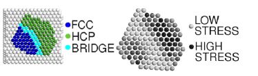
Submonolayer regime. - In the submonolayer regime, we performed GO for several island sizes (). Consistently with the experimentally observed layer-by-layer growth Liu99 ; deSiervo05A , all the global minimum energy structures for are flat. A low energy structure for is shown in Fig.1. It is worth noticing that the adsorption energy of the island does not substantially depend on its stacking. When the Pd slab has stacking sequence ABC, the Cu atoms in the next layer can occupy sites A or B, which are referred to as fcc or hcp stackings, respectively Carter95 ; Hamilton95 . The potential correctly assigns a lower cohesion energy to fcc than to hcp bulk, although the difference is small, meV/atom. The best adsorption site for a single Cu atom on Pd(111) is on the fcc site, the energy difference from the hcp stacking being meV. Consequently, islands with are completely on the fcc sites. All the larger islands, where are in both fcc and hcp stackings.
A stress color-scale graph is shown in Fig. 1. The stress of atom is quantified as the isostatic local atomic pressureNielsen83 ; Vitek87 ; Ouahab05 , where runs over the neighbors of atom is the total potential energy of the system and is the distance between and . The tensile stress is largest near the center of the fcc and hcp domains and stress release originates from partial dislocations running along the domain walls.
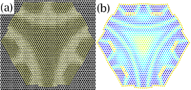
In similar systems exhibiting 2D incommensurate ordering, the walls are called heavy or superheavy, corresponding to atoms at neighbor fcc and hcp sites or atoms on bridge positions, respectively Zeppenfeld88 . The latter are more common in islands. In our system both walls are often distorted to bring atoms closer to the equilibrium distance. Especially the superheavy walls are typically curved and extended over several lattice spacings. While the wall atoms are at disadvantageous positions, the elastic relaxation, which would not be possible without the domain structure, has longer range and releases energy in the whole island. Larger hexagonal islands also display the domains in a pattern which is called a trigon Hamilton95 . The center of the trigon shows energy increase due to high stress levels, as shown in Fig.2(b).
Monolayer regime. - Although we find that pseudomorphic Cu at 1 ML coverage, which is shown in Fig.3, panel A, is stable upon local energy minimization, both GO and AM methods can locate lower energy structures. They consist of alternating fcc and hcp stacking domains similar to the submonolayer islands. We will refer to these structures collectively as the fcc-hcp domain configurations (cf. Fig. 2). We are thus led to investigate what is the stability of the pseudomorphic film relative to the fcc-hcp domains and to what extent the adsorbate is epitaxial.
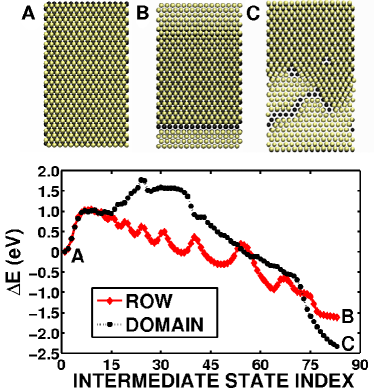
To mimic the row dislocation networks sometimes reported from similar systems Schaff01 , we perturb the simulation cell by pushing a directional row of the Cu layer Å down to the negative direction. We activate the system with only 3 layers of Pd, but after finding a transition path, we increase the substrate thickness to 9 by adding 6 layers below the originals. As before, the two bottom of the enlarged system are kept frozen. The AM then yields a configuration where the overlayer has contracted and split to reveal an directional row from the substrate, see Fig. 3, panel B. This row dislocation state has lower energy than the pseudomorphic state and contains fcc-hcp domains, but the energy barrier exceeds eV.
The fcc-hcp domains both in the submonolayer islands and from the GO runs at 1 ML seem to have a fairly irregular structure. To estimate the energy barrier connecting the pseudomorphic layer to these structures, we pushed randomly selected Cu atoms Å to the nearest edge direction. The result after the AM procedure also shows fcc-hcp domains, see Fig. 3, panel C. These domains have striking similarity to what is described in Refs. Carter95, ; Hamilton95, ; Gabaly05, ; Hwang97, ; Figuera01, ; Schmid97, ; Gunther95, . The energy path connecting the pseudomorphic state to the fcc-hcp domain is characterized by multiple large barriers which exceed the row dislocation barrier. The holes on the overlayer are now better aligned to allow stress release in several directions (cf. Fig. 2, panels B and C). Because the row dislocation shows the stacking domains and the energy barrier is in the same range as in the disordered case, it is possible to view it as a special case which also belongs to the fcc-hcp domain class.
The NEB energy paths of Fig. 3 suggest that if a uniform pseudomorphic overlayer can be formed, high energy barriers will prevent the decay into the fcc-hcp domain structure. If this overlayer was grown with conventional deposition methods, some adatoms would eventually land on the film. Therefore we are led to ask if a few adatoms on a single pseudomorphic layer would be enough to activate a defect nucleation.
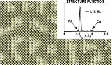
In our initial state we placed Cu adatoms, all at the same time, on top of a pseudomorphic layer at randomly selected fcc stacking positions. Substrate layer sizes and were used with increasing . We find that with simple energy minimization spontaneously incorporate into the interfacial layer. For all the cases considered saturates near the number difference between the fully pseudomorphic and fully relaxed layers, which is roughly times the layer size. The remaining Cu adatoms stay in the topmost layer. As a result of the incorporation, a fcc-hcp domain structure is again formed, as shown in Fig.4. In saturation, the fcc stacking is slightly more frequent than hcp. GO runs also display similar low-energy patterns. Overlayer structures with fcc-hcp domains similar to those in Fig. 2 have been observed on various heteroepitaxial systems on (111) surfaces Hamilton95 .
Discussion. - The results presented here are in agreement with the experimentally reported layer-by-layer growth of Cu on Pd(111) Oral90 ; Liu99 ; deSiervo05A , since flat islands are the low energy configurations in the whole submonolayer range considered here. However, our results predict that the most favorable arrangement of Cu on top of Pd(111) is the fcc-hcp domain configuration rather than an epitaxial configuration. This result was obtained both from the global optimization method as well as from the activated and spontaneous relaxation starting from a perfect epitaxial state.
The experimental peak intensities from Auger electron spectroscopy (AEG), low energy electron spectroscopy (LEED) Oral90 and reflection high energy electron diffraction (RHEED) deSiervo05A were interpreted to indicate that the Cu deposition is epitaxial up to ML. In contrast, in our calculations fcc-hcp domain configurations occur already at the submonolayer regime. In the measured RHEED intensities, however, there is a Cu-like peak already visible and distinguishable from the Pd-like at ML deSiervo05A . To estimate the degree of epitaxy in the overlayers exhibiting fcc-hcp domains, we plot the average structure function averaged over eight configurations after incorporation at 1.18 ML coverage in Fig.4. The averaging is done to remove the dependence on the random adatom positions. Most of the signal is Pd-like because both the fcc and hcp domains are nearly coherent with the substrate. However, there is some relaxation originating from the domain walls and this produces two peaks near the ideal Cu-like location, corresponding to distorted heavy and superheavy walls. After averaging the Cu-peaks are less visible and for realistic temperatures the fluctuations would further smear the data. If the Pd signal slope were changing faster than the slope of the Cu signal as a function of the wave vector length the latter signal would be difficult to resolve. However, there is no reason why the morphology could not change to completely relaxed layers from the domain structure after deposition of a few layers, as the experimental data shows. Thus, in our view, the existence of the stacking domains is not ruled out by the experiments.
Similar fcc-hcp domains have been observed experimentally in Cu/Ru(0001) with misfit Gabaly05 ; Hwang97 ; Figuera01 ; Schmid97 ; Gunther95 . Theoretical studies suggest that the existence of the structure is not sensitive to details of the stressed fcc(111) system Carter95 ; Hamilton95 . Instead, these structures arise from the existence of two favorable states, fcc and hcp sites, and from the competition between strain energy relief and the energy cost for dislocation formation. The loss of epitaxy of Cu/Ru(0001) occurs above 1 ML coverage but in our system with misfit the critical coverage is below ML, which is in line with the higher stress level. In the Cu/Pd(111) system the incorporation would not lead to further stress release because the layer is already patterned below ML. However, in the Cu/Ru(0001) system the process is visible. The XPS intensity data for Cu/Pd(111) system also leave room for layer-by-layer morphology above ML deSiervo05A .
Conclusion. - We have used computational approach to understand the structure of Cu films on the Pd(111) surface in the low coverage regime extending from -atom islands to ML. Our results agree with layer-by-layer growth, as is observed experimentally. Our model predicts that the epitaxiality is lost already below ML coverage and Cu forms hcp and fcc stacking domains, separated by wall regions in which Cu recovers its lattice spacing and releases its tensile stress. This pattern, similar to what is seen in Cu/Ru(0001) at higher coverages, encourages further experimental investigations directly probing the overlayer structure.
Acknowledgements. - This work has been supported in part by the Academy of Finland through the COMP CoE grant, CSC-IT Center of Science Ltd. through allocation of computer resources, and joint funding under EU STREP Grant No. 016447 MagDot and NSF DMR Grant No. 0502737. J.J. acknowledges support from the Finnish Cultural Foundation. E.G. was supported by Fundação de Amparo á Pesquisa do Estado de São Paulo - FAPESP (Grant no. 07/08492-9).
References
- (1) F. El Gabaly, W. L. W. Ling, K. F. McCarthy and J. de la Figuera, Science 27, 1303 (2005).
- (2) R. Q. Hwang and M. C. Bartelt, Chem. Rev. 97, 1063 (1997).
- (3) J. de la Figuera, A. K. Schmid, N. C. Bartelt, K. Pohl and R. Q. Hwang Phys. Rev. B 63, 165431 (2001).
- (4) A. K. Schmid, N. C. Bartelt, J. C. Hamilton, C. B. Carter and R. Q. Hwang Phys. Rev. Lett. 78, 3507 (1997).
- (5) C. Günther, J. Vrijmoeth, R. Q. Hwang and R. J. Behm, Phys. Rev. Lett. 74, 754 (1995).
- (6) C. B. Carter and R. Q. Hwang, Phys. Rev. B 51, 4730 (1995).
- (7) J. C. Hamilton and S. M. Foiles, Phys. Rev. Lett. 75, 882 (1995).
- (8) R. Pushpa and S. Narasimhan, Phys. Rev. B 67, 205418 (2003).
- (9) In fcc(111) geometry the simplest defect arrangements whose Burgers vectors cancel at distance are pairs pointing to opposite directions or triplets radiating from a common centre. The meeting points of partial dislocations belong to either of these categories and the general features of the resulting domain structure can be expected to be insensitive to details of the interactions.
- (10) Annealing the Cu/Pd(111) system above K leads to formation of a surface alloy Liu99 ; deSiervo05B , which is more stable than the pseudomorphic film. At room temperature this is not seen and is supposedly behind a considerable kinetic barrier, in which case the local stress release processes considered here have a lower activation energy.
- (11) G. Liu, T. P. St. Clair and D. W. Goodman, J. Phys. Chem. B 103, 8578 (1999).
- (12) A. de Siervo, R. Paniago, E.A. Soares, H.-D. Pfannes, R. Landers and G.G. Kleiman, Surf. Sci. 575, 217 (2005).
- (13) B. Oral and R.W. Vook, J. Vac. Sci. Technol. A 8, 3048 (1990).
- (14) A. de Siervo, E. A. Soares, R. Landers and G. G. Kleiman, Phys. Rev. B 71, 115417 (2005).
- (15) M. S. Daw and M. I. Baskes, Phys. Rev. B 29, 6443 (1984).
- (16) S. M. Foiles, M. I. Baskes and M. S. Daw, Phys. Rev. B 33, 7983 (1986).
- (17) Y. Lu, M. Przybylski, O. Trushin, W. H. Wang, J. Barthel, E. Granato, S. C. Ying and T. Ala-Nissila Phys. Rev. Lett. 94, 146105 (2005).
- (18) Z-X. Chen, K. M. Neyman, A. B. Gordienko, and N. Rosch, Phys. Rev. B 68, 075417 (2003).
- (19) C. Mottet, G. Tréglia and B. Legrand, Phys. Rev. B 66, 045413 (2002).
- (20) G. Rossi and R. Ferrando, J. Phys.: Condens. Matter. 21, 084208 (2009).
- (21) D. J. Wales, in Energy Landscapes with Applications to Clusters, Biomolecules and Glasses, (Cambridge University Press, Cambridge, 2003).
- (22) J. Jalkanen, O. Trushin, E. Granato, S.C. Ying and T. Ala-Nissila, Phys. Rev. B 72, 081403(R) (2005).
- (23) O. Trushin, J. Jalkanen, E. Granato, S. C. Ying and T. Ala-Nissila, J. Phys.: Condens. Matter 21, 084211 (2009).
- (24) O. Trushin, E. Granato, S.-C. Ying, P. Salo and T. Ala-Nissila, Phys. Stat. Sol. B, 232,100 (2002).
- (25) O.S. Trushin, P. Salo, T. Ala-Nissila, and S.C. Ying, Phys. Rev. B. 69, 033405 (2004).
- (26) H. Jónsson, G. Mills and K. W. Jacobsen, in Classical and Quantum Dynamics in Condensed Phase Simulations, ed. by B. J. Berne et al (World Scientific, Singapore, 1998).
- (27) O. Schaff, A. K. Schmid, N. C. Bartelt, J. de la Figuera and R. Q. Hwang, Mater. Sci. Eng., A 319, 914 (2001)
- (28) O. H. Nielsen and R. M. Martin, Phys. Rev. Lett. 50, 697 (1983).
- (29) V. Vitek and T. Egami, Phys. Stat. Sol. (b) 144, 145 (1987).
- (30) A. Ouahab, C. Mottet and J. Goniakowski, Phys. Rev. B 72, 035421 (2005).
- (31) P. Zeppenfeld, K. Kern, R. David and G. Comsa, Phys. Rev. B 38, 3918 (1988).