Hysteresis Switching Loops in Agmanganite memristive interfaces
Abstract
Multilevel resistance states in silvermanganite interfaces are studied both experimentally and through a realistic model that includes as a main ingredient the oxygen vacancies diffusion under applied electric fields. The switching threshold and amplitude studied through Hysteresis Switching Loops are found to depend critically on the initial state. The associated vacancy profiles further unveil the prominent role of the effective electric field acting at the interfaces. While experimental results validate main assumptions of the model, the simulations allow to disentangle the microscopic mechanisms behind the resistive switching in metaltransition metal oxide interfaces.
Introduction
Manganese based oxides with perovskite structure (manganites) are one of the promising families of transition metal oxides that exhibit resistive switching (RS) phenomena waser ; sawa ; waser2 i.e a reversible and nonvolatile change in the resistance after the application of a pulsed electric stimulus (voltage or current). In addition to two well distinguishable “on” and “off” resistance values, multilevel memory states are found. beck This property, together with demonstrated downsizing possibilities, low power consumption and high speed switching, qualify manganite based devices as possible candidates for resistance random access memories (RRAM), motivating a huge amount of experimental activity. baek ; liu ; beck ; watanabe ; choi In contrast, few theoretical publications shed light on the microscopic mechanisms behind the RS in oxide compounds. ris ; ris2 ; real ; jeong ; waser2 ; nian ; tulina ; chae
Recent experimental evidence indicates that the RS effect in metal-manganite devices is due to the memristive properties of the interface between the metallic electrode and the oxide.hp Memresistance is a property of a material that amounts to a past-history dependence of the current magnitude of its resistance. chua This effect at the interfaces is believed to be driven by the redistribution of oxygen vacancies under the action of the applied electric fields. sawa ; szot ; seong ; nian ; real In the specific case of conductive manganites, the presence of oxygen vacancies severely disrupts Mn-O links, enhancing the resistivity. nian A positive electric pulse applied at one electrode may cause the migration of oxygen vacancies located in the vicinity of the interface, producing a decrease of the contact resistance, due essentially to the recomposition of Mn-O links. nian On the other hand, negative electric pulses produce vacancies at the interface by repelling oxygen ions.
The Hysteresis Switching Loop (HSL) is a protocol for electrical measurements which was shown to be a powerful tool to test the role of oxygen vacancies in RS phenomena. nian The HSL consists on the measurement of the remnant resistance state (read operation) obtained after pulsing (write operation) in a loop sequence (i.e., apply increasing positive pulses up to a maximum value, after which the amplitude is decreased, then the polarity is reversed until a negative maximum is reached, to finally return back to zero). The remnant resistance state is measured after every pulse by means of a small bias current. Here we study such resistance states at silver manganite interfaces, focusing on their multilevel capabilities.
Our experimental results show that the switching threshold and switching resistance amplitude are both non-trivially determined by the past resistance history of the interface, suggesting that the local distribution of vacancies near the contact oxide interface might determine the main features of the switching response. Based on the model proposed in Ref.real, , that incorporates as a key ingredient the migration of oxygen vacancies in a nanoscale vicinity of the metal oxide interfaces, we perform numerical simulations that reproduce the experimental data remarkably well and provide important confirmation to the theoretical assumptions of the model. They indicate that the migration of oxygen vacancies is produced due to the strong electric fields that build up at the electrode-manganite interface, and is at the origin of the most significant resistive changes. This fact could provide valuable guidance to decrease and optimize the strength of stimulus threshold required for switching in practical devices.
Experimental Results
We study silver - manganite interfaces by means of a 3 terminal procedure. Millimeter sized contacts were hand painted on top of a bulk polycrystalline sample. A scheme of the electrical contacts is depicted in the inset of Fig.1. Electric pulses and bias current are applied through A and D contacts, and voltage measurements are independently acquired at the respective terminals. Here we show only results obtained for the D pulsed electrode. Measurements at the A pulsed contact are qualitatively similar and show complementary behavior with respect to contact D quintero ; marlasca . Pulsing was performed with a Keithley 2400 source - meter, while remnant data were acquired with an Agilent 34407 data acquisition / switch unit.
Initially, to induce RS on the virgin sample, a set of pulses of a given amplitude and polarity is applied between electrodes A and D, followed by a similar set with the opposite polarity quintero ; marlasca , and repeating the procedure several times. After this, pulsing in a loop mode (i.e. the HSL) was the electrical protocol used to switch the interface resistance nian ; marlasca (write operation). Each squared pulse of 10 ms time width was followed by a small bias applied some 10 seconds after the pulse to obtain the remnant resistance curve (read operation). Heating effects appear to be negligible, as determined from dynamic measurements.
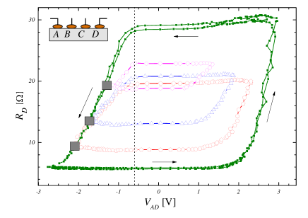
Figure 1 depicts the resistance values for the interface at electrode D as a function of the pulsing voltage strength applied between electrodes A and D. is the small bias current applied after each pulsing. We begin the pulsing protocol by performing a major loop that corresponds to the maximal pulsed-voltage excursion. As observed, the resistance exhibits two well defined states (around 30 and 6 ), namely the high H and low L resistance states, and two rapid transitions through a multitude of stable intermediate states.
Starting at the L state, we observe a certain threshold voltage of positive pulsing stimulus, 2 V, that is required to initiate the rapid upward change in the resistance. The total resistive switching produces a factor - of - five change in . Once the H state has been achieved at the maximal positive pulsing strength, the loop mode tests the stability of the state against pulses of gradually decreasing amplitude and then its coercivity, i.e. the stability against pulses of opposite polarity with increasing strength.
We observed negligible changes in while the polarity of the stimulus remains positive. More significantly, the interface resistance also shows a significant coercivity, as the transition from H to L only begins when a small but non-zero negative pulsing is applied (indicated by a vertical dashed line in Fig.1).
During the rapid transition, the interface traverses a multitude of different resistance states which are all (meta)stable as we shall see later on. This feature is a clear signature of the memristive properties of the interface.
Eventually the L resistance value is reached at the maximum negative polarity pulsing, and it remains stable through the rest of the loop. This is, both, when decreasing negative pulses towards zero, but also upon changing to positive polarity and increasing the pulsing strength up to . Again, this fact demonstrates the significant coercivity of the resistance state. Interestingly, the values of and have different magnitudes and also, as we shall see below, different dependence on the applied voltages. This is not surprising, due to the directional asymmetry of the ionic migration at a each interfacial region.
Upon repeating the HSL protocol, a second major loop is formed almost perfectly on top of the previous one, demonstrating a good reproducibility and control of the memristive effect at the interfaces of our device.
To further characterize the intermediate multilevel states during the H to L transition, additional measurements were performed sequentially ranging the pulsing stimulus between lower voltage limits (i.e. ”minor loops”). Different initial states on the major loop were used for starting each of the minor loops. After measuring a set of three minor loops for a given voltage excursion, always a set of three new major loops were performed to reset the system. All loops of the same set (minors and major) showed similar reproducibility characteristics as the one already shown for the first major loop. Therefore, for the sake of clarity we only show in Fig.1 a representative minor loop for each set.
As observed, upon performing minor loops, new sets of intermediate stable L and H resistance states are obtained. Note that these new L states have the same value of the initial intermediate state. The corresponding H value is found to be always lower than that of the major loop. Additional aspects of these sequentially obtained data are to be pointed out:
-
1.
The stability of the multilevel intermediate resistance states is clearly established. Minor loops have the same qualitative shape as the major one, their actual H/L (or ON/OFF) resistance ratio being proportional to the sweep range of the stimulus. In addition, the reversible character of the complete sequence of a major loop followed by a minor one is remarkable.
-
2.
For positive stimulus, the threshold for switching is higher when the initial state resistance is lower. Note that this resistance value becomes the L state of the corresponding minor loop.
-
3.
However, for negative stimulus the situation is different. The dotted line on Fig.1 indicates that upon reversing the pulsing polarity, the remnant resistance starts decreasing at a voltage value that is almost independent of the initial resistance level.
We now turn to the comparison of these experimental results with simulations performed using the model introduced in Ref.real, .
Model Simulations
We here describe the main ingredients that built up the theoretical model together with the basic equations employed in the numerical simulations. For further details we refer the reader to Ref.real, .
The model mimics the active region for conduction as a one dimensional resistive network, or chain, of links, each one characterized by a certain concentration of oxygen vacancies. This 1d model may be considered as a drastic simplification of the actual 3d geometry. However, this assumption is supported by the fact that experimental evidence indicate that the conduction in the low resistance state is highly inhomogeneous, and takes place along preferential and directional paths sawa .
The first and last links define the left (L) and right (R) interfacial regions between each metallic electrode and the bulk material (B) that is described by links.
The main idea behind the model is that the local oxygen vacancy concentration of a domain, , determines the resistance of the respective network link . The constants relate vacancy concentration and resistivity, and depend on the material and on the region. In principle the could be computed from a microscopic approach that incorporates geometrical and material specific information. This important but technically challenging issue is beyond the scope of the present phenomenological modeling. The constants are defined as if belongs to the bulk (), if is in the left interface () and if is in the right interface (). The parameters are taken to be to stress that both interfaces are much more resistive than the bulk region. Indeed, experiments indicate that a Schottky type of barrier formed between a metallic electrode and the oxide could be the origin of the contact resistance fujii ; sawa2 ; chen . The total two terminal resistance is defined as , where is a geometrical factor that we take equal to unity without loss of generality.
Under an external applied stimulus (typical experimental voltage or current protocols), the voltage drops at the network domains create local electric fields that promote the diffusive motion of the positive charged oxygen vacancies. In order to specify the model equations we shall consider as the stimulus a given voltage protocol applied between L and R electrodes (see below).
The local dynamics for the diffusion of vacancies is ruled by the following equation,
| (1) |
that specifies the probability for transfer of vacancies from domain to a nearest neighbor domain .
The probability Eq.1, is proportional to the concentration of vacancies present in domain , and to the concentration of “available vacancy sites” at the neighbor domain. In addition, Eq.1 is also proportional to the Arrhenius factor , where is a dimensionless constant related to the activation energy for vacancies diffusion and is the local potential drop with .
Starting from an initial vacancy concentration profile , the numerical simulations are performed through the following steps: (i) at each simulation time step a given external voltage is applied between the electrodes, that are assumed as perfect conductors, (ii) we compute the local voltage profile and the voltages drops . (iii) we use Eq. (1) to compute all the oxygen vacancy transfers between nearest neighboring domains, and update the values to a new set of concentrations . (iv) we use these new values to recompute at time the local resistivities and the local voltage drops under the applied voltage , as indicated in the first step.
A crucial outcome of the model real is that the local electric fields created in the vicinity of the interfacial regions are much more intense than in the bulk. Thus as we shall show below, the motion of vacancies is enhanced in the vicinity of the interfaces, producing dramatic changes in its local resistivities. As a consequence, the change in the two terminal resistance, , are mainly due to variations of the interfacial resistances, . This is in perfect agreement with the experimental findings that suggest the interfaces as the active regions for resistive switching. nian ; quintero ; ignatiev ; chen
To compare results obtained by model simulations with the experimental ones already described, we shall concentrate on the right interfacial resistance , that by analogy corresponds to the interface in contact to the D electrode in the experimental set up. Following Ref.real, , in our simulations we take the total number of sites where the first and last sites define the L and R interfaces respectively. We analyze a symmetric configuration, assuming identical interfaces for both (Ag) electrodes, setting . In addition we choose , to provide a non-negligible but slow diffusive contribution to the evolution of .
Comparison with experimental data
Figure 2 shows in a solid line a HSL of the resistance as a function of applied voltage protocol . Each cycle is defined by a linear ramp of time steps of duration and , to supply a sufficiently large electric stimulus. note
The agreement with the experimental HSL obtained in Fig.1 is evident. As the voltage is increased from , and after surpassing the threshold value (marked by dot 1 in Fig.2) the high resistance state H is stable and is attained at Vmax, while multiple states are traversed in between, i.e. during the transition from L to H. The H state remains stable when decreasing the voltage from V. Significantly, it also remains stable after the inversion of polarity and up to a small but finite threshold that is indicated with the dot 3. Similarly to the experimental case described before, beyond the transition from H to L state starts and the interface goes through a multitude of stable states of decreasing resistance. At the maximum negative voltage, the interface reaches the L state of lowest resistance. Then, it remains stable as the voltage is ramped up from V, and also after the voltage polarity inversion up to the . Notice, however, that the new loop does not go precisely on top of the previous one. Thus upon starting a new cycle for the same voltage sequence, a small offset is obtained in the resistance values. We shall come back to this point later when discussing the evolution of the vacancies profiles.
Simulations of minor loops response were also performed ranging the voltage profile in a sequence . The different initial values indicated by the squares in Fig.2 , where chosen along the major loop in order to mimic the experimental protocol. Each starting point has associated a particular vacancy profile that works as the initial state for the numerical simulations that produce each minor HSL, identified in Fig.2 with different traces.
Interestingly, several qualitative features of intermediate states in the simulated HSL reproduce nicely the experimental findings. The value of the predicted voltage threshold for L to H transition in the model decreases for higher initial resistance values (i.e. higher resistance of the L state). In addition, we also observe that the threshold voltage for the H to L transition is almost independent of the H resistance value. These two features are in good qualitative agreement with our experimental findings described above.
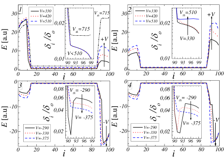
Finally, it is interesting to correlate this switching behavior with the respective evolutions of vacancy profiles and local electric fields that develop along the conductive path.
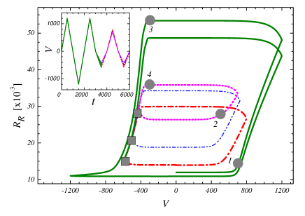
Figure 3 depicts the electric field profile along the sample, where is the applied voltage and is the total two-terminal resistance. The data of the figure corresponds to states that are close to the thresholds values for the L to H (panels 1) and 2)) and H to L (panels 3) and 4)) transitions for the selected major and minor loops (panel numbers correlate with the points indicated in Fig.2). In coincidence with previous studies real , Fig.3 shows that the interfaces are the regions in which locally enhanced electric fields built up and promote the motion of vacancies. On the other hand, due to the metallic character of the bulk and its lower resistivities (), negligible electric fields act well inside the bulk region. However, the accumulation of vacancies near the transition regions L-B and R-B lead to significant field in the first few links that enter the bulk real . This feature can be clearly seen in the insets of each panel of Fig.3. The continuity and penetration of the field E across these internal interfaces allows for migration of vacancies to and from the bulk reservoir.
We shall concentrate in the vacancy profiles along the R interface, but a similar analysis could be done for the left interface. In the respective insets of Fig.3, we plot the vacancy concentration profiles (normalized to the constant initial value ) along the R interface (sites 90 to 100).
Below we shall analyze how vacancies and electric field profiles evolve close to the L(H) to H(L) HSL transition.
In panels 1) and 2) of Fig.3 we compare the vacancies and electric field profiles for values of close to the threshold and (dot 1 and 2 respectively in Fig.2) for the L to H transitions. We observe that at the respective threshold voltages, the vacancies density profiles of the relevant R interfacial region saturate in both cases to a constant value. This is the state reached before vacancies start to migrate out of the resistive interface into the much less resistive bulk. Notice that the constant value is higher in (2) than in (1), corresponding to the higher resistance value of the L state in the minor loop respect to the major one.
Comparing the local electric field at the R interface, we find that a similar value a.u. is attained at both L to H transitions. In addition we have also checked that the same values of are obtained for other minor HSL at the respective L to H transitions. Taking into account that in our simulations we have taken as the activation energy for diffusion, this value of provides a significant migration of vacancies into the R interface in order to produce the L to H transition in the different HSL.
Note in addition that, for the different values of applied , the local electric field at the R interface exhibits important relative variations in comparison to the left interface. This shows that the switching process occurs rather independently at each interface and that the switching occurs fast when the threshold level is reached.
Although at both threshold voltages the local electric fields at the R interface have rather similar values, at the left interface, in panel 1) almost duplicates the values in panel 2). This accounts for a higher value of the threshold voltage in panel 1) as compared to panel 2).
Next, we focus on the H to L transition. Vacancy and electric field profiles for the states labeled by dots 3 and 4 in Fig.2 are depicted respectively in panels 3) and 4) of Fig.3, for three values of close to the threshold voltage for the H to L transition in both HSL. Electric field profiles look qualitatively similar for all ’s investigated. The large (and negative) values of along the R interface are a signature of the H resistance state. In addition due to the similar electric field profiles along the whole sample the same threshold value () is obtained for both H to L transition in panels 3) and 4), in remarkable agreement with the experimental data.
Vacancy profiles shown in the insets of panels 3) and 4) of Fig.3 are also qualitatively similar, although the profile in 3) exhibits a higher and broader distribution than in 4), consistent with a higher resistance value.
Note that the vacancy profiles for both L to H transitions (panels 1) and 2)) are quite smooth, while those for the H to L transitions (panels 3) and 4)) are sharper and non monotonic. Thus the H resistance state in each HSL has associated a rather complex vacancy distribution as a consequence of the enhanced internal electric field at the interface.
Upon cycling periodically, a small concentration of vacancies that migrate from the interfaces towards the bulk remain confined at the bulk due to relatively small electric fields acting at the bulk. Once there, they no longer contribute to interfacial switching. This explains the small offset in the resistance values obtained, experimentally and in the simulations, in the HSL after each cycle is completed (see Figs.1 and 2). This effect is possibly responsible for the long time degradation of the switching ON/OFF ratio. A systematic study of this feature is therefore important and will be the focus of future work.
Recently, Das et al. studied the threshold stimulus dependence for switching in manganite thin films with Ag contacts by injecting pulses of opposite polarity. das They obtain a sample to sample variation, and they emphasize the sigmoid like (universal) character of the dependence of the RS behavior with the applied stimulus das . In addition, our results suggest that the choice of the initial state, i.e. the resistance value within the H to L transition branch of the major loop, is a key parameter in order to determine both, threshold stimulus value, and the resistive ON/OFF ratio. We have also demonstrated a full control of these features as we were always able to restore back the system from any minor loop to the major one.
Final remarks
Multilevel resistance states in pulsed Ag- manganite contacts have been directly related to different oxygen vacancy profiles and local electric fields at the interface. The strong dependence of the threshold stimulus on the initial state is a signature of the role played by detrapping or electric field enhanced migration of oxygen vacancies in the underlying RS mechanism.
As a summary, we list main findings of this work:
- stable multilevel states exhibiting RS are obtained and controlled experimentally following a loop pulsing procedure;
- a remarkable qualitative agreement between experimental and simulated data has been obtained, providing further validation to the model introduced in Ref.real, .
- control of RS switching characteristics such as ON/OFF ratio and coercivity were demonstrated.
Our results suggest that different initial vacancy configurations could be tailored by the application of other voltage protocols than the one used here for the major loop. Thus one may conceive that an optimal low threshold stimulus for a given desired ON/OFF switching ratio could be obtained. Moreover, the model validation shown here opens the way for a rapid testing of other initial vacancy configurations, suggesting alternative electro forming-like procedures. We believe that our work demonstrates the usefulness of theoretical modeling of the resistive switching phenomena as a valuable aid to provide guidance in the analysis of the experimental results and, eventually, for the design and optimization of memory devices.
Acknowledgements.
Support from CONICET (grants PIP 5254/05 and PIP 112-200801-00047) and ANCTyP (grants PICT 483/06 and PICT 837/07) is gratefully acknowledged. We thank R. Weht for his contribution in the early stage of this work. MJS, PL and MJR are members of CONICET.References
- (1) R. Waser and M. Aono, Nature Materials 6, 833 (2007).
- (2) A. Sawa, Materials Today 11, 28 (2008).
- (3) R. Waser, R.Dittmann, G.Staikov and K.Szot, Adv. Mater 21, 2632 (2009).
- (4) A. Beck et al., App. Phys. Lett. 77, 139 (2000).
- (5) I. G. Baek et al., Tech. Dig. IEDM. 587 (2004).
- (6) S. Q. Liu, N. J. Wu, and A. Ignatiev, Appl. Phys. Lett. 76 2749 (2000).
- (7) Y. Watanabe et al., App. Phys. Lett. 78, 3738 (2001).
- (8) B. J. Choi et al., J. Appl. Phys. 98, 033715 (2005).
- (9) M. J. Rozenberg, I. H. Inoue and M. J. Sánchez, Phys. Rev. Lett. 92, 178302 (2004).
- (10) M. J. Rozenberg, I. H. Inoue and M. J. Sánchez, Appl. Phys. Lett. 88, 033510 (2006).
- (11) M. J. Rozenberg et al., Phys. Rev. B. 83 in press (2010), cond-mat/10010703.
- (12) D. S. Jeong, H. Schroeder and R. Waser, Phys. Rev. B. 79, 195317 (2009).
- (13) Z. Szot et al., Nat. Mater. 5, 312 (2006).
- (14) D. -J. Seong et al., Electrochem. Solid-State Lett. 10 H168 (2007).
- (15) Y. B. Nian et al., Phys. Rev. Lett. 98, 146403 (2007).
- (16) N. A. Tulina, Phys. Usp. 50 1171 (2007).
- (17) S. C. Chae et al., Adv. Mater. 20 1154 (2008).
- (18) D. B. Strukov et al., Nature 80, 453 (2008).
- (19) I. O. Chua, IEEE Trans. Circuit Theory CT-18. 507 (1971).
- (20) F. Gomez-Marlasca and P. Levy, J. Phys.: Conf. Ser. 167, 012036 (2009).
- (21) T. Fujii et al., Appl. Phys. Lett. 86, 012107 (2005).
- (22) A. Sawa et al., Appl. Phys. Lett. 85 4073 (2004).
- (23) X. Chen et al., Appl. Phys. Lett. 87 233506 (2005).
- (24) M. Quintero et al., Phys. Rev. Lett. 98 116601 (2007).
- (25) A. Ignatiev et al., Phase Transitions 81, 791, (2008).
- (26) In the numerical simulations the calculated values of resistance at each simulation time step corresponds to the experimental resistance that is measured with the small bias current.
- (27) N. Das et al, Phys. Rev. B 80, 115411 (2009).