The successful fabrication of single layer graphene has greatly stimulated the progress of the research on graphene. In this article, focusing on the basic electronic and transport properties of graphene nanoribbons (GNRs), we review the recent progress of experimental fabrication of GNRs, and the theoretical and experimental investigations of physical properties and device applications of GNRs. We also briefly discuss the research efforts on the spin polarization of GNRs in relation to the edge states.
Towards Graphene Nanoribbon-based Electronics
I Introduction
Graphene, one monolayer of carbon atoms tightly packed into a two-dimensional honeycomb lattice, is actively being pursued as a material for next-generation electronics due to its promising electronic properties, such as high carrier mobility Novoselov-S04 ; Berger-JPCB , long phase coherence lengths Berger . On the other side, the unique two-dimensional atomic structure of graphene implies unique confinement on electron system and offers a perfect platform to explore the amazing physics phenomenons, such as quantum Hall effect Gusynin ; Novoselov-S07 ; Zhang ; Novoselov-N05 and massless Dirac fermions Novoselov-N05 ; Zhou-NP06a ; Bostwick ; Andrei ; Park-NP ; Li-NP08 .
The first task for experimentalists to study graphene electronics is to fabricate high quality single layer graphene. Until now, several different experimental methods have been proposed and realized to prepare single layer (or few layers) graphene, including mechanical exfoliation of highly oriented pyrolytic graphite Novoselov-S04 , patterned epitaxially grown graphene on silicon carbide or transition metal (e.g. Ru, Ni) substrates Berger-JPCB ; D. Usachov ; Sutter ; D. Martoccia , liquid-phase exfoliation of graphite Hernandez ; Fan ; Tung , substrate-free gas-phase synthesis Dato , and chemical vapor deposition Reina ; Kim-N09 . The success in fabricating single layer graphene has stimulated the extensive research efforts (both theoretical and experimental) in graphene related research area.
The ultimate goal of the use of graphene in next-generation electronics is to realize all-graphene circuit with functional devices built from graphene layers or graphene nanoribbons (GNRs) Areshkin-07b ; Qimin . As the basic building blocks of such circuit, the concept of electronic devices based on graphene have been proposed theoretically and realized by experiments recently, such as field effect transistors Qimin ; Liang ; Meric ; Song , p-n junctions J. R. Williams ; D. A. Abanin-pn ; B. oyilmaz ; Gorbachev , gas molecule sensor F. Schedin ; Wehling ; J. T. Robinson , and so on.
In this article, we will focus our discussion on the basic electronic and transport properties of GNRs and their application to electronic devices. In particular, the theoretical investigations of GNRs physics and the technical aspects of GNR based electronic devices will be reviewed in detail. For other topics on the recent experimental and theoretical research efforts on graphene, please refer to the reviews by Katsnelson Katsnelson-MT , Geim et al. A. K. Geim , Beenakker Beenakker , and Castro Neto et al. A. H. Castro Neto ,
II Experimental Fabrication of Graphene Nanoribbons
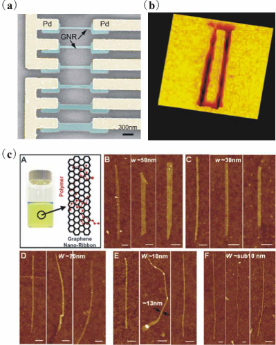
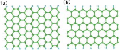
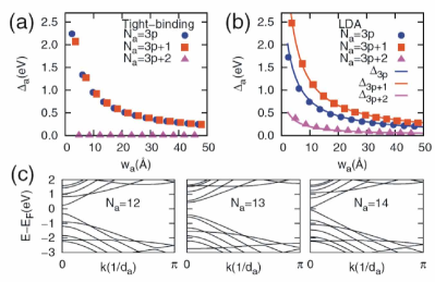
The realization of graphene electronics relies on the ability to modify the electronic properties of finite-size graphenes (for example, from semiconducting to metallic) by varying their size, shape, and edge orientation. Such unique property compared to traditional semiconductor materials, such as silicon, would ultimately enable the design and miniaturization of future electronic circuit by patterned graphene. One of the most important issues in patterned graphene fabrication is the control of the nanoribbon width. In order to take advantage of quantum confinement effects in graphene, the ribbon width should go down to nanometer scale. To realize the patterning of graphene with nano-scale width, several different techniques have been proposed including standard e-beam lithography (Fig. 1a) Han ; Chen , microscope lithography (Fig. 1b) L. Tapaszto ; Weng ; Giesbers , chemical method (Fig. 1c) Dai-Science , metallic nanoparticle etching Datta1 , and e-beam irradiation of ultrathin poly(methylmethacrylate) (PMMA) Duan . As shown in Fig. 1a, the scanning electron microscopy (SEM) image reveals the graphene can be patterned by traditional e-beam lithography technique into nanoribbons with various widths ranging from 20 to 500 nm Chen . Figure 1b shows 10-nm-wide nanoribbon etched via scanning tunnelling microscope (STM) lithography. By setting the optimal lithographic parameters, it is possible to cut GNRs with suitably regular edges, which constitutes a great advance towards the reproducibility of GNR-based devices L. Tapaszto . Figure 1c shows atomic force microscopy images of chemically derived GNRs with various widths ranging from 50 nm to sub-10 nm. These GNRs have atomic-scale ultrasmooth edges Dai-Science .
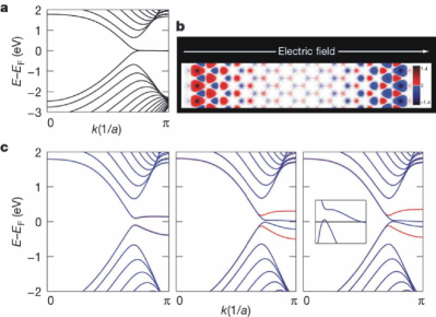
The electronic properties of GNRs exhibit a strong dependence on the orientation of their edges. As two typical types, armchair GNRs (AGNRs) and zigzag GNRs (ZGNRs) can be obtained by lithography technology along the specific orientation on graphene (Fig. 2b) Han ; L. Tapaszto . Actually, the detailed edge structures (both armchair and zigzag) have already been clearly observed in recent experiments Kobayashi ; Y. Niimi ; Zheng Liu . One of the most serious obstacle to graphene electronic application is the reliable control of the edge structure of GNRs. Theoretical studies predict that edge states (in a manner similar to the well-known concept of surface states of a 3D crystal) in graphene are strongly dependent on the edge termination and affect the physical properties of GNRs Qimin ; K. Nakada ; K. Wakabayashi ; Y. Miyamoto ; Son-PRL ; Barone ; Gunlycke-PRB08 . However, until now there is no reliable experimental method which is able to exactly control the edge structures and reduce their roughness. An interesting experimental observation is that the band gaps of GNRs show little orientation dependence Han and all fabricated GNRs show semiconducting behavior Dai-PRL , which seems inconsistent with theoretical results K. Nakada ; K. Wakabayashi ; Y. Miyamoto . One of the reason for such inconsistency comes from the roughness of GNR edges and our explanation is also given in the following part of the article. Another issue related to GNR edges is the edge passivation. Since the dangling bonds from the edge carbon atoms have relatively high chemical activity, there is the possibility that other chemical elements present in the material fabrication process (such as C, O, N, H and other chemical groups formed by these atoms) would interact with the edge atoms and modify the electronic properties of GNRs. To the best of our knowledge, this issue has not been properly solved experimentally.
III Elementary Electronic and Transport Properties of Graphene Nanoribbons
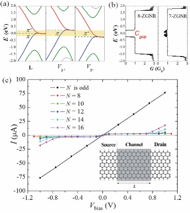
Next we will review some basic electronic and transport properties of GNRs from the theoretical viewpoint. Figs. 2a and 2b show two typical models of armchair and zigzag GNRs in first-principles or other atomic-level electronic structure calculations, noting as 11-AGNR and 6-ZGNR, respectively. Here the numbers 11 and 6 are defined as the width index, . In order to remove the effect of dangling bonds, the edges of GNRs are saturated by hydrogen atoms. As geometrically terminated graphene, the electronic structure of GNRs can be modelled by imposing appropriate boundary conditions on Schrödinger’s equation with simple tight-binding (TB) approximations based on -states of carbon K. Nakada ; K. Wakabayashi . Another way to get the band structure is to solve two-dimensional Dirac’s equation of massless free particles with an effective speed of light to model GNR system L. Brey . Within these models, it is predicted that GNRs with armchair-shaped edges can be either metallic or semiconducting depending on their widths, as shown in Fig. 3a. On the other side, the GNRs with zigzag-shaped edges are metallic with peculiar edge states on both sides of ribbons regardless of their widths, as shown in Fig. 4a. K. Nakada ; K. Wakabayashi ; Son-Nature
Further detailed ab initio and GW quasiparticle calculations show that all of the AGNRs exhibit semiconducting behavior and the energy gaps decrease as a function of increasing ribbon widths. The variation in energy gaps can be separated into three distinct family behaviors Son-PRL ; Barone ; Qimin ; YangLi-GW , as shown in Fig. 3b. As mentioned above, such dependence of band gap on the geometrical structure of GNR offers unique possibility to modify the electronic properties of GNRs simply by controlling the width and edge orientation in order to realize all-graphene functional devices.
Upon inclusion of the spin degrees of freedom within density functional theory (DFT) calculations, ZGNRs are predicted to have a magnetic insulating ground state with ferromagnetic ordering at each zigzag edge and antiparallel spin orientation between the two edges Son-PRL ; Son-Nature , as shown in Fig. 4b. The spin polarization originates from the edge states that introduce a high density of state (DOS) at the Fermi energy. It can be qualitatively understood in terms of the stoner magnetism of electrons (in analogy to conventional electrons), which occupy a very narrow edge band and render instability of spin-band splitting Bing . What is more interesting, the zigzag GNRs show half-metallic behavior when external transverse electric field is applied across the ZGNRs along the lateral direction Son-Nature , as shown in Fig. 4c. However, such spin related half-metallic phenomenon becomes weak with increasing ribbon width (since the total energy difference per edge atom between spin-unpolarized and spin-polarized edge states is only about 20 meV in their simulation system and decreases with increasing width) and is not energetically stable if the width of GNR is significantly larger than the decay length of the spin-polarized edge states Kan-APL ; Rudberg . On the other hand, it is predicted that the half-metallicity can be also achieved in edge-modified or doped ZGNRs Hod ; Kan-JACS ; Sodi ; Dutta
Another important issue regarding the basic electronic structures of GNRs relies on the edge states. Due to the presence of the edge states, the and subbands of metallic ZGNRs (in the spin-unpolarized state) do not cross with each other at the Fermi level to span the whole energy range like metallic armchair carbon nanotubes (CNTs) (the left panel of Fig. 5a). This leads to the fact that the transport property of ZGNRs under a low bias voltage (or a small potential step) is only determined by the transmission between and subbands (as shown in Fig. 5a). With the presence of such unique band structures, ZGNRs exhibit two distinct transport behaviors depending on the existence of mirror symmetry with respect to the midplane between two edges Zuanyi ; Cresti ; Akhmerov ; Nakabayashi , although all the ZGNRs have similar metallic energy band structures. Since the and subbands of symmetric ZGNRs (i.e., width index is an even number) have opposite definite parities, the transmission between them is forbidden (the left panel of Fig. 5b). For asymmetric ZGNRs (i.e., width index is an odd number), however, their and subbands do not have definite parities, so the coupling between them can contribute to about one conductance quantum (the right panel of Fig. 5b). This transport difference can be clearly reflected in the current-bias-voltage (-) characteristics of ZGNRs by using the first-principle transport simulation, as shown in Fig. 5c. Although metallic armchair carbon nanotubes also have and subbands with definite parities, such symmetry-depending (or band-selective) - characteristics cannot be observed in them because of the crossover of their subbands, i.e., the absence of edge states. Recently, theoretical work predicts a very large magnetoresistance in a graphene nanoribbon device due to the existence of edge states Woo .
Besides the fabrication and theoretical study of monolayer graphene and GNRs, recent experimental Novoselov-bilayer ; E. Rotenberg ; E. V. Castro and theoretical M. I. Katsnelson ; Kai-Tak Lama ; Eduardo V. Castro ; Sahu-08 studies are also carried out on bilayer graphene and GNRs. Theoretically, it is shown that the bilayer GNRs and monolayer GNRs have some similar electronic properties such as edge states localized at the zigzag edges and semiconducting behavior of armchair bilayer GNRs Kai-Tak Lama ; Eduardo V. Castro ; Sahu-08 . Experimentally, it is found that the bilayer graphene has unique features such as anomalous integer quantum Hall effects Novoselov-bilayer , which is absent in single layer graphene. And the size of energy gap of such bilayer structures can be controlled by adjusting carrier concentration E. Rotenberg as well as by an external electric field E. V. Castro . These unique properties open an opportunity to implement bilayer graphene or GNRs in various electronic applications.
IV Edge disorder in Graphene Nanoribbons
As mentioned above, current experimental techniques (such as lithography) are not able to realize exact control of the edge structures of GNRs and the edges are always very rough due to the limitation of the fabrication technology Han ; Chen . There are theoretical evidences that such edge disorders can significantly change the electronic properties of GNRs Areshkin ; Gunlycke ; Querlioz ; TCLi ; Lherbier ; Cresti-NaR , and lead to some unexpected physics effect, such as the Anderson localization M. Evaldsson ; E. R. Mucciolo and Coulomb blockade effect F. Sols . These effects have already been observed in lithographically obtained graphene nanoribbons B. oyilmaz ; Han ; Stampfer-APL ; Stampfer-PRL ; Kathryn Todd .
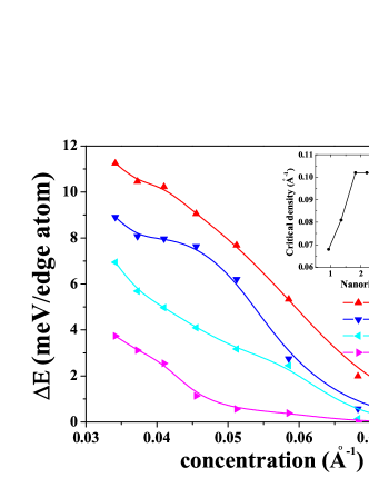
The edge roughness is also crucial for the spin polarized properties of GNRs. As we know, the magnetic properties of GNRs depend on the highly degenerate edge states. In principle a perfect edge structure is necessary for stabilizing magnetic properties of GNRs as theoretically predicted. An important question is, how robust the spin-polarized state is in the presence of edge defects and impurities? The answer to this question is not only scientifically interesting to better understand the physical mechanism of spin polarization in GNRs but also has important technological implications in the reliability of GNRs as a new class of spintronic materials. First-principles theoretical studies reveals the effect of edge vacancies and substitutionally doped boron atoms, as typical examples of structural edge defects and impurities, on the spin-polarization of ZGNRs Bing . The calculated energy difference between the magnetic state [both antiferromagnetic (AF) and ferromagnetic (FM)] and the nonmagnetic state is found to rapidly decrease with increasing defect concentration and eventually decrease to zero (nonmagnetic), as shown in Fig. 6. The critical defect (impurity) concentration is found to be 0.10/Å when the ribbon width is larger than 2 nm.
Evidently, the magnetism in GNRs depends on a high density of state (DOS) around the Fermi energy coming from the highly degenerate edge states in a perfect ribbon edge () that renders instability of spin polarization Bing . The presence of edge vacancies and impurities would decrease the DOS at since they do not contribute to the same edge state. From Stoner model, such decrease of DOS will suppress the spin polarization of GNR systems. Therefore, the practical realization of the spin polarization in GNRs for spintronics applications could be rather challenging Bing . Recently, an interesting theoretical work systematically studied the spin current in rough GNRs and predicted that only GNRs with imperfect edges exhibit a nonzero spin conductance while there is no spin current in perfect GNRs Wimmer . It confirms that the edge effect is of great importance to spin related properties of GNRs.
Furthermore, the problem of edge passivation has not yet clearly resolved by experiment until now. From the theoretical viewpoint, the edge passivation can be well modeled by the modifications of the hopping energies in the tight-binding approach Novikov or via additional phases in the boundary conditions Kane . Recent theoretical modeling and calculations have indicated that the edge passivation has a strong effect on the electronic and spin-polarized properties of GNRs Hod ; Kan-JACS ; Sodi . The possible passivation species include hydrogen, carbon, oxygen, nitrogen, and other chemical groups. Further experimental works are needed to explore the realistic edge structures of GNRs at atomic scale and determine which types of edge passivation are favorable.
V Transistors based on Graphene Nanoribbons
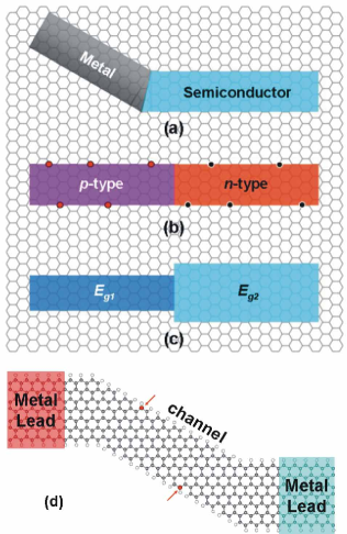
The interesting and unique electronic properties of GNRs, such as orientation and width dependence of transport behavior, offer great possibilities for their electronic device applications. Compared with other electronic materials, one of the most promising advantage of GNRs is that GNR-based devices and even integrated circuits can be fabricated by a single process of patterning a graphene sheet Qimin . Figures 7a-7c illustrate three basic device building blocks: (i) metal-semiconductor junction, (ii) p-n junction, and (iii) hetero-junction, which can be, respectively, made by patterned GNRs (i) along different direction, (ii) with different edge doping, and (iii) with different widths. It was proposed that a variety of devices can be constructed from these building blocks. For example, a field effect transistor (FET) can be made simply by two metal-semiconductor junctions, as shown in Fig. 7d. There are some potential key advantages in designing and constructing device architectures based on GNRs. The first advantage is the perfect atomic interface, a feature that is difficult to achieve for the interconnection between nanotubes of different diameter and chirality. Second, it is generally difficult to find a robust method to make contact with the molecular device unit, because there exists usually a large contact resistance between the metal electrodes and molecules (e.g., single-walled CNT) due to a very small contact area. This difficulty may be circumvented by using GNRs, because the GNR-based devices can be connected to the outside circuits exclusively via metallic GNRs (or graphene), as illustrated in Fig. 7d, which serve as extensions of metal electrodes to make contact with the semiconducting GNRs so that an atomically smooth metal-semiconductor interface is maintained with minimum contact resistance. Last but not the least, the edges of GNRs may serve as effective sites for doping. In principle, by introducing different types of dopants at different sections of GNR edges, one can realize a p-n junction by selective doping, as shown in Fig. 7b.
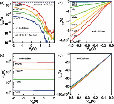
One of the most important electronic applications based on GNRs is field effect transistors. Recently, experimental studies Han ; Chen ; Dai-Science ; Dai-PRL have indicated the possibility of fabricating GNR-based transistors. The advantage of GNRs as an alternative material for transistors is that it could bypass the chirality challenge of CNTs while retaining the excellent electronic properties of graphene sheets, such as the high / ratio and excellent electron/hole mobilities. The performance of one sub-10-nm GNR-FET in the latest work from Dai’s group is shown in Figs. 8a and 8b (the transfer and output characteristics, respectively, for the GNR device with the width of 2 0.5 nm and the channel length of 236 nm)Dai-PRL . This device delivered 4 A at = 1 V, / ratio 106 at = 0.5 V, subthreshold slope =d/ 210 mV/decade and transconductance 1.8 S (900 S/m). The device performance is comparable with the best CNT-based transistors. However, the Dirac point was not observed around zero gate bias in this measurement, indicating p-doping effects at the edges or by physisorbed species during the chemical treatment steps.
Together with experimental progress on GNR-based transistors, theoretical studies using semiclassical and quantum transport models show that GNR-based FETs could have a similar performance as CNT-based FETs and might outperform traditional Si-based FETs Qimin ; Ouyang-APL06 ; Liang-JAP ; Ryzhii . Figure 9 shows a first-principles study on the performance of a typical GNR-based FET made with a 5.91 nm long intrinsic semiconducting 10-AGNR channel connected to two metallic 7-ZGNR leads (source and drain) Qimin . In Fig. 9a, the near-symmetric curve shows an excellent ambipolar transistor with ON/OFF ratio / 2000 and subthreshold swing of 60 mV/decade, which are comparable to those of high performance CNT-FETs. Such the field effect can be clearly reflected in the change of characteristics under different gate voltages (Fig. 9b). Figure 9c shows the curves of the GNR-FETs made from the same 10-AGNR channel with its length ranging from 1.69 to 6.76 nm, from which the values of are derived as a function of as shown in Figure 9d. Clearly, decreases with increasing , and gradually approaches 60 mV/decade when becomes longer than 6 nm. Meanwhile, the ON-current stays the same, independent of , but the OFF-state leakage current increases rapidly with decreasing , which gives rise to a large . The performance of the ambipolar GNR-FETs made of intrinsic semiconductor channels can be understood in terms of metal-semiconductor tunneling junctionh within the semiclassical band-bending model.
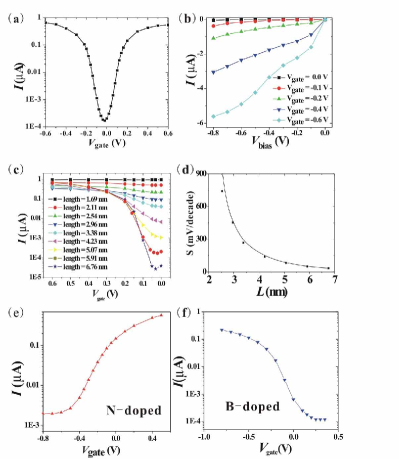
Compared with the basic ambipolar FETs, it is well known that n-type (or p-type) FETs serve as critical transistor devices for digital electronics applications Avouris ; Dai-Nanolett . To realize such device design based on GNRs, a method was proposed using N (or B) atoms as selective dopants at the channel region of perfect GNR-FETs (the positions of B or N are indicated by arrows in Fig. 7d). Figure 9e (9f) shows the calculated curves under = 20 mV, exhibiting the typical behavior of a n-type (p-type) FETQimin . It is suggested that all of the functional transistor devices that work in traditional Si-based circuits could be realized by GNRs and GNR-based junctions in principle.
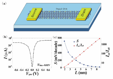
Noting the current experimental difficulty to get an accurate Z-shape junction (i.e., FET shown in Fig. 7d) due to the limitation of lithography technique, a new type of field effect transistor has also been proposed taking advantage of the metal-semiconductor transition in ZGNRs induced by substitutional doping of nitrogen or boron atoms at their edges Bing-APL , as shown in Fig. 10a. Besides simplifying the fabrication process, such a linear configuration can also increase the device density in electronic circuits. Figure 10b shows a typical curve for the N-doped GNR-FET (with the channel length of 8.54 nm) under the bias voltage = 0.01 V. Clearly, the doped FET exhibits ambipolar characteristics, similar to the Z-shape FETs. The relationship between the device performance and the channel length is demonstrated by calculating curve of N-doped GNR-FETs as a function of the doped channel length while keeping the bias voltage at 0.01 V. As shown in Fig. 10c, the subthreshold swing of these doped GNR-FETs decreases and the ON/OFF current ratio increases exponentially. It can be seen that for good device performance with small value (e.g., below 100 mV/decade) and high ON/OFF current ratio (e.g., above 100), the doped channel length should be longer than 5 nm. The minimum leakage current of those FETs with the doped channels shorter than this critical length will be greatly enhanced by direct tunneling, which lowers the device performance.
Besides ideal case, some more practice issues concerning GNR-based FETs are discussed in recent theoretical works. For example, the effects of the various contact types and shapes on the performance of Schottky-barrier-type GNR-FETs have been investigated theoretically Liang-NaL , which indicates that the semi-infinite normal metal can potentially provide promising performance. In addition, the effect of edge roughness and carrier scattering on GNR-FETs have been studied Yoon ; Basu ; Ouyang . The presence of edge disorder significantly reduces ON-state currents and increases OFF-state currents (the ON/OFF ratio decreases), and introduces wide variability across devices. These effects become weaker for GNRs with larger width and smoother edges. However, the band gap decreases with increasing width, thereby increasing the band-to-band tunneling mediated subthreshold leakage current even with perfect GNRs. Obviously, without atomically precise edge control during fabrication, it is hard to get reliable and stable performance of GNR-FETs.
Due to their unusual basic properties, GNRs as well as graphene are promising for a large number of applications A. K. Geim ; Cresti-NaR , from spin filters Wimmer ; Fazzio ; Kan-JACS , valley filters Rycerz , to chemical sensors F. Schedin ; J. T. Robinson ; Bing-JPCC . GNRs can be chemically and/or structurally modified in order to change its functionality and hence its potential applications.
VI Summary
In summary, we review the basic electronic and transport properties of graphene nanoribbons, and discuss recent theoretical and experimental progress on GNR-based field effect transistors from the viewpoint of device application. Due to the interesting electronic and magnetic properties, GNRs have been demonstrated as a promising candidate material for future post-silicon electronics such as transport materials, field effect transistors, and spin injection or filter. More experimental efforts will focus on fabricating high quality nanoribbon samples with accurate control of the edge structures.
Acknowledgements.
This work was supported by the Ministry of Science and Technology of China (Grant Nos. 2006CB605105 and 2006CB0L0601), and the National Natural Science Foundation of China.References
- (1) K. S. Novoselov, A. K. Geim, S. V. Morozov, D. Jiang, Y. Zhang, S. V. Dubonos, I. V. Grigorieva, and A. A. Firsov, Science 306, 666 (2004).
- (2) C. Berger, Z. Song, T. Li, X. Li, A. Y. Ogbazghi, R. Feng, Z. Dai, A. N. Marchenkov, E. H. Conrad, P. N. First, and W. A. de Heer, J. Phys. Chem. B 108, 19912 (2004).
- (3) C. Berger, Z. Song, X. Li, X. Wu, N. Brown, C. Naud, D. Mayou, T. Li, J. Hass, A. N. Marchenkov, E. H. Conrad, P. N. First, and W. A. de Heer, Science 312, 1191 (2006).
- (4) V. P. Gusynin, and S. G. Sharapov, Phys. Rev. Lett. 95, 146801 (2005).
- (5) K. S. Novoselov, Z. Jiang, Y. Zhang, S. V. Morozov, H. L. Stormer, U. Zeitler, J. C. Maan, G. S. Boebinger, P. Kim, and A. K. Geim, Science 315, 1379 (2007).
- (6) Y. Zhang, Y. W. Tan, H. L. Stormer, and P. Kim. Nature (London) 438, 201 (2005).
- (7) K. S. Novoselov, A. K. Geim, S. V. Morozov, D. Jiang, M. I. Katsnelson, I. V. Grigorieva, S. V. Dubonos, and A. A. Firsov, Nature (London) 438, 197 (2005).
- (8) S. Y. Zhou, G.-H. Gweon, J. Graf, A. V. Fedorov, C. D. Spataru, R. D. Diehl, Y. Kopelevich, D.-H. Lee, S. G. Louie, and A. Lanzara, Nature Phys. 2, 595 (2006).
- (9) A. Bostwick, T. Ohta, T. Seyller, K. Horn, and E. Rotenberg, Nature Phys. 3, 36 (2007).
- (10) G. Li and E. Y. Andrei, Nature Phys. 3, 623 (2007).
- (11) C.-H. Park, L. Yang, Y.-W. Son, M. L. Cohen, and S. G. Louie, Nature Phys. 4, 213 (2008).
- (12) Z. Q. Li, E. A. Henriksen, Z. Jiang, Z. Hao, M. C. Martin, P. Kim, H. L. Stormer, and D. N. Basov, Nature Phys. 4, 532 (2008).
- (13) D. Usachov, A. M. Dobrotvorskii, A. Varykhalov, O. Rader, W. Gudat, A. M. Shikin, and V. K. Adamchuk, Phys. Rev. B 78, 085403 (2008).
- (14) P. W. Sutter, J. Flege, and E. A. Sutter, Nature Mater. 7, 406 (2008).
- (15) D. Martoccia, P. R. Willmott, T. Brugger, M. Bjorck, S. Gunther, C. M. Schleputz, A. Cervellino, S. A. Pauli, B. D. Patterson, S. Marchini, J. Wintterlin, W. Moritz, and T. Greber, Phys. Rev. Lett. 101, 126102 (2008).
- (16) Y. Hernandez, V. Nicolosi, M. Lotya,F. M. Blighe, Z. Sun, S. De, I. T. McGovern, B. Holland, M. Byrne, Y. K. Gunko, J. J. Boland, P. Niraj, G. Duesberg, S. Krishnamurthy, R. Goodhue, J. Hutchison, V. Scardaci, A. C. Ferrari, and J. N. Coleman, Nat. Nanotechnol. 3, 563 (2008).
- (17) X. Fan, W. Peng, Y. Li, X. Li, S. Wang, G. Zhang, and F. Zhang, Adv. Mater. 20, 4490 (2008).
- (18) V. C. Tung, M. J. Allen, Y. Yang, and R. B. Kaner, Nat. Nanotechnol. 4, 25 (2009).
- (19) A. Dato, V. Radmilovic, Z. Lee, J. Phillips, and M. Frenklach, Nano Lett. 8, 2012 (2008).
- (20) A. Reina, X. Jia, J. Ho, D. Nezich, H. Son, V. Bulovic, M. S. Dresselhaus, and J. Kong, Nano Lett. 9, 30 (2009).
- (21) K. S. Kim, Y. Zhao, H. Jang, S. Y. Lee, J. M. Kim, K. S. Kim, J.-H. Ahn, P. Kim, J.-Y. Choi, B. H. Hong, Nature (London) 457, 706 (2009).
- (22) D. A. Areshkin, and C. T. White, Nano Lett. 7, 3253 (2007).
- (23) Q. Yan, B. Huang, J. Yu, F. Zheng, J. Zhang, J. Wu, B.-L. Gu, F. Liu, and W. Duan, Nano Lett. 7, 1469 (2007).
- (24) X. Liang, Z. Fu, and S. Y. Chou, Nano Lett. 7, 3840 (2007).
- (25) I. Meric, M. Y. Han, A. F. Young, B. Ozyilmaz, P. Kim, and K. L. Shepard, Nat. Nanotechnol. 3, 654 (2008).
- (26) X. Wu, M. Sprinkle, X. Li, F. Ming, C. Berger, and Walt A. de Heer, Phys. Rev. Lett. 101, 026801 (2008).
- (27) J. R. Williams, L. DiCarlo, and C. M. Marcus, Science 317, 638 (2007).
- (28) D. A. Abanin and L. S. Levitov, Science 317, 641 (2007).
- (29) B. Öyilmaz, P. Jarillo-Herrero, D. Efetov, D. A. Abanin, L. S. Levitov, and P. Kim, Phys. Rev. Lett. 99, 166804 (2007).
- (30) R. V. Gorbachev, A. S. Mayorov, A. K. Savchenko, D. W. Horsell, and F. Guinea, Nano Lett. 8, 1995 (2008).
- (31) F. Schedin, A. K. Geim, S. V. Morozov, E. W. Hill, P. Blake, M. I. Katsnelson, and K. S. Novoselov, Nature Mater. 6, 652 (2007).
- (32) T. O. Wehling, K. S. Novoselov, S. V. Morozov, E. E. Vdovin, M. I. Katsnelson, A. K. Geim, and A. I. Lichtenstein, Nano Lett. 8, 173 (2008).
- (33) J. T. Robinson, F. K. Perkins, E. S. Snow, Z. Wei, and P. E. Sheehan, Nano Lett. 8, 3137 (2008).
- (34) M. I. Katsnelson, Mater. Today 10, 20 (2007).
- (35) A. K. Geim and K. S. Novoselov, Nature Mater. 6, 183 (2007).
- (36) C. W. J. Beenakker, Rev. Mod. Phys. 80, 1337 (2008).
- (37) A. H. Castro Neto, F. Guinea, N. M. R. Peres, K. S. Novoselov, and A. K. Geim, Rev. Mod. Phys. 81, 109 (2009).
- (38) M. Y. Han, B. Öyilmaz, Y. Zhang, and P. Kim, Phys. Rev. Lett. 98, 206805 (2007).
- (39) Z. Chen, Y.-M. Lin, M. J. Rooks, and P. Avouris, Physica E 40, 228 (2007).
- (40) L. Tapasztó, G. Dobrik, P. Lambin, and L. P. Biró, Nat. Nanotechnol. 3, 397 (2008).
- (41) L. Weng, L. Zhang, Y. P. Chen, and L. P. Rokhinson, Appl. Phys. Lett. 93, 093107 (2008).
- (42) A. J. M. Giesbers, U. Zeitler, S. Neubeck, F. Freitag, K.S. Novoselov, J. C. Maan, Solid St. Comm. 147, 366 (2008).
- (43) X. Li, X. Wang, L. Zhang, S. Lee and H. Dai, Science 319, 1229 (2008).
- (44) S. S. Datta, D. R. Strachan, S. M. Khamis, and A. T. Charlie Johnson, Nano Lett. 8, 1912 (2008).
- (45) H. Duan, E. Xie, L. Han, and Z. Xu, Adv. Mater. 20, 3284 (2008).
- (46) Y. Kobayashi,1, K. Fukui, T. Enoki, K. Kusakabe, and Y. Kaburagi, Phys. Rev. B 71, 193406 (2005).
- (47) Y. Niimi, T. Matsui, H. Kambara, K. Tagami, M. Tsukada, and H. Fukuyama, Phys. Rev. B 73, 085421 (2006).
- (48) Z. Liu, K. Suenaga, Peter J. F. Harris, and S. Iijima, Phys. Rev. Lett. 102, 015501 (2009).
- (49) K. Nakada, M. Fujita, G. Dresselhaus and M. S. Dresselhaus, Phys. Rev. B 54, 17954 (1996).
- (50) K. Wakabayashi, M. Fujita, H. Ajiki, and M. Sigris, Phys. Rev. B 59, 8271 (1999).
- (51) Y. Miyamoto, K. Nakada, and M. Fujita, Phys. Rev. B 59, 9858 (1999).
- (52) Y. -W. Son, M. L. Cohen, and S. G. Louie, Phys. Rev. Lett. 97, 216803 (2006).
- (53) V. Barone, O. Hod, and G. E. Scuseria, Nano Lett. 6, 2748 (2006).
- (54) D. Gunlycke and C. T. White, Phys. Rev. B 77, 115116 (2008).
- (55) X. Wang, Y. Ouyang, X. Li, H. Wang, and H. Dai, Phys. Rev. Lett. 100, 206803 (2008).
- (56) L. Brey, and H. A. Fertig, Phys. Rev. B 73, 235411 (2006).
- (57) Y.-W. Son, M. L. Cohen, and S. G. Louie, Nature (London) 444, 347 (2006).
- (58) L. Yang, C.-H. Park, Y.-W. Son, M. L. Cohen, and S. G. Louie, Phys. Rev. Lett. 99, 186801 (2007).
- (59) B. Huang, F. Liu, J. Wu, B.-L. Gu, and W. Duan, Phys. Rev. B 77, 153411 (2008).
- (60) E.-J. Kan, Z. Li, J. Yang, and J. G. Hou, Appl. Phys. Lett. 91, 243116 (2007).
- (61) E. Rudberg, P. Sałek, and Y. Luo, Nano Lett. 7, 2211 (2007).
- (62) O. Hod, V. Barone, J. E. Peralta, and G. E. Scuseria, Nano Lett. 7, 2295 (2007).
- (63) E.-J. Kan, Z. Li, J. Yang, and J. G. Hou, J. Am. Chem. Soc. 130, 4224 (2008).
- (64) F. Cervantes-Sodi, G. Csányi, S. Piscanec, and A. C. Ferrari, Phys. Rev. B 77, 165427 (2008).
- (65) S. Dutta and S. K. Pati, J. Phys. Chem. B 112, 1333 (2008).
- (66) Z. Li, H. Qian, J. Wu, B.-L. Gu, and W. Duan, Phys. Rev. Lett. 100, 206802 (2008).
- (67) A. R. Akhmerov, J. H. Bardarson, A. Rycerz, and C. W. J. Beenakker, Phys. Rev. B 77, 205416 (2008).
- (68) A. Cresti, G. Grosso, and G. Pastori Parravicini, Phys. Rev. B 77, 233402 (2008).
- (69) J. Nakabayashi, D. Yamamoto, and S. Kurihara, Phys. Rev. Lett. 102, 066803 (2009).
- (70) W. Y. Kim, and K. S. Kim, Nat. Nanotechnol. 3, 408 (2008).
- (71) K. S. Novoselov, E. McCann, S. V. Morozov, V. I. Falko, M. I. Katsnelson, U. Zeitler, D. Jiang, F. Schedin, and A. K. Geim, Nat. Phys. 2, 177 (2006).
- (72) T. Ohta, A. Bostwick, T. Seyller, K. Horn, and E. Rotenberg, Science 313, 951 (2006).
- (73) E. V. Castro, K. S. Novoselov, S. V. Morozov, N. M. R. Peres, J. M. B. Lopes dos Santos, J. Nilsson, F. Guinea, A. K. Geim, and A. H. Castro Neto, Phys. Rev. Lett. 99, 216802 (2007).
- (74) M. I. Katsnelson, K. S. Novoselov, and A. K. Geim, Nat. Phys. 2, 620 (2006).
- (75) K.-T. Lam and G. Liang, Appl. Phys. Lett. 92, 223106 (2008).
- (76) E. V. Castro, N. M. R. Peres, J. M. B. Lopes dos Santos, A. H. Castro Neto, and F. Guinea, Phys. Rev. Lett. 100, 026802 (2008).
- (77) B. Sahu, H. Min, A. H. MacDonald, and S. K. Banerjee, Phys. Rev. B 78, 045404 (2008).
- (78) D. A. Areshkin, D. Gunlycke, and C. T. White, Nano Lett. 7, 204 (2007).
- (79) D. Gunlycke, D. A. Areshkin, and C. T. White, Appl. Phys. Lett. 90, 12104 (2007).
- (80) D. Querlioz, Y. Apertet, A. Valentin, K. Huet, A. Bournel, S. Galdin-Retailleau, and P. Dollfus, Appl. Phys. Lett. 92, 042108 (2008).
- (81) T. C. Li, and S.-P. Lu, Phys. Rev. B 77, 085408 (2008).
- (82) A. Lherbier, B. Biel, Y.-M. Niquet, and S. Roche, Phys. Rev. Lett. 100, 036803 (2008).
- (83) A. Cresti, N. Nemec, B. Biel, G. Niebler, F. Triozon, G. Cuniberti, and S. Roche, Nano Res. 1, 361 (2008).
- (84) M. Evaldsson, I. V. Zozoulenko, H. Xu, and T. Heinzel, Phys. Rev. B 78, 161407 (2008).
- (85) E. R. Mucciolo, A. H. Castro Neto, and C. H. Lewenkopf, Phys. Rev. B 79, 075407 (2009).
- (86) F. Sols, F. Guinea, and A. H. Castro Neto, Phys. Rev. Lett. 99, 166803 (2007).
- (87) C. Stampfer, J. Güttinger, F. Molitor, D. Graf, T. Ihn, and K. Ensslin, Appl. Phys. Lett. 92, 012102 (2008).
- (88) C. Stampfer, J. Güttinger, S. Hellmüller, F. Molitor, K. Ensslin, and T. Ihn, Phys. Rev. Lett. 102, 056403 (2009).
- (89) K. Todd, H.-T. Chou, S. Amasha, and D. Goldhaber-Gordon, Nano Lett. 9, 416 (2009).
- (90) M. Wimmer, I. Adagideli, S. Berber, D. Tomanek, and K. Richter, Phys. Rev. Lett. 100, 177207 (2008).
- (91) D. S. Novikov, Phys. Rev. Lett. 99, 056802 (2007).
- (92) C. L. Kane, and E. J. Mele, Phys. Rev. Lett. 78, 1932 (1997).
- (93) Y. Ouyang, Y. Yoon, J. K. Fodor, and J. Guo, Appl. Phys. Lett. 89, 203107 (2006).
- (94) G. Liang, N. Neophytou, M. S. Lundstrom, and D. E. Nikonov, J. Appl. Phys. 102, 054307 (2007).
- (95) V. Ryzhii, M. Ryzhii, A. Satou, and T. Otsuji, J. Appl. Phys. 103, 094510 (2008).
- (96) P. Avouris, Acc. Chem. Res. 35, 1026 (2002).
- (97) A. Javey, J. Guo, D. B. Farmer, Q. Wang, D. Wang, R. G. Gordon, M. Lundstrom, and H. Dai, Nano Lett. 4, 447 (2004).
- (98) B. Huang, Q. Yan, G. Zhou, J. Wu, B.-L. Gu, W. Duan, and F. Liu, Appl. Phys. Lett. 91, 253122 (2007).
- (99) G. Liang, N. Neophytou, M. S. Lundstrom, and D. E. Nikonov, Nano Lett. 8, 1819 (2008).
- (100) Y. Yoon and J. Guo, Appl. Phys. Lett. 91, 073103 (2007).
- (101) D. Basu, M. J. Gilbert, L. F. Register, S. K. Banerjee, and A. H. MacDonald, Appl. Phys. Lett. 92, 042114 (2008).
- (102) Y. Ouyang, X. Wang, H. Dai, and J. Guo, Appl. Phys. Lett. 92, 243124 (2008).
- (103) T. B. Martins, R. H. Miwa, A. J. R. da Silva, and A. Fazzio, Phys. Rev. Lett. 98, 196803 (2007).
- (104) A. Rycerz, J. Tworzydło, and C. W. J. Beenakker, Nature Phys. 3, 172 (2007).
- (105) B. Huang, Z. Li, Z. Liu, G. Zhou, S. Hao, J. Wu, B.-L. Gu, and W. Duan, J. Phys. Chem. C 112, 13442 (2008).