Abstract
The discovery of a metallic state and a metal-insulator transition (MIT) in two-dimensional (2D) electron systems challenges one of the most influential paradigms of modern mesoscopic physics, namely, that “there is no true metallic behavior in two dimensions”. However, this conclusion was drawn for systems of noninteracting or weakly interacting carriers, while in all 2D systems exhibiting the metal-insulator transition, the interaction energy greatly exceeds all other energy scales. We review the main experimental findings and show that, although significant progress has been achieved in our understanding of the MIT in 2D, many open questions remain.
Chapter 0 A metal-insulator transition in 2D:
Established facts and open questions
In 2D electron systems, the electrons move in a plane in the presence of a weak random potential. According to the scaling theory of localization of Abrahams et al. [1], these systems lie on the boundary between high and low dimensions insofar as the metal-insulator transition is concerned. The carriers are always strongly localized in one dimension, while in three dimensions, the electronic states can be either localized or extended. In the case of two dimensions the electrons may conduct well at room temperature, but a weak logarithmic increase of the resistance is expected as the temperature is reduced. This is due to the fact that, when scattered from impurities back to their starting point, electron waves interfere constructively with their time reversed paths. Quantum interference becomes increasingly important as the temperature is reduced and leads to localization of the electrons, albeit on a large length scale; this is generally referred to as “weak localization”. Indeed, thin metallic films and many of the two-dimensional electron systems fabricated on semiconductor surfaces display the predicted logarithmic increase of resistivity.
The scaling theory [1] does not consider the effects of the Coulomb interaction between electrons. The strength of the interactions is usually characterized by the dimensionless Wigner-Seitz radius,
(here is the electron density and is the Bohr radius in a semiconductor). As the density of electrons is reduced, the Wigner-Seitz radius grows and the interactions provide the dominant energy of the system. In the early 1980’s, Finkelstein [2, 3] and Castellani et al. [4] found that for weak disorder and sufficiently strong interactions, a 2D system scales towards a conducting state as the temperature is lowered. However, the scaling procedure leads to an increase in the effective strength of the spin-related interactions and to a divergent spin susceptibility, so that the perturbative approach breaks down as the temperature is reduced toward zero. Therefore, the possibility of a 2D metallic ground state stabilized by strong electron-electron interactions was not seriously considered at that time, particularly as there were no experimental observations to support the presence of a metallic phase.
Progress in semiconductor technology has enabled the fabrication of high quality 2D samples with very low randomness in which measurements can be made at very low carrier densities. The strongly-interacting regime () has thus become experimentally accessible. The first observation of a metal-insulator transition in strongly-interacting, low-disordered 2D systems on a silicon surface was reported in 1987 by Zavaritskaya and Zavaritskaya [5]. Although identified by the authors as a metal-insulator transition, the discovery went by unnoticed. Subsequent experiments on even higher mobility silicon samples [6, 7, 8, 9, 10] confirmed the existence of a metal-insulator transition in 2D and demonstrated that there were surprising and dramatic differences between the behavior of strongly interacting systems with as compared with weakly-interacting systems. These results were met with great skepticism and were largely overlooked until they were confirmed in other strongly-interacting 2D systems in 1997 [11, 12, 13, 14, 15, 16]. Moreover, it was found [17, 18, 19, 20] that in the strongly-interacting regime, an external in-plane magnetic field strong enough to polarize the spins of the electrons or holes induces a giant positive magnetoresistance and completely suppresses the metallic behavior, implying that the spin state is central to the high conductance of the metallic state. Recent experiments [21, 22, 23, 24, 25, 26, 27, 28] have shown that there is a sharp enhancement of the spin susceptibility as the metal-insulator transition is approached. Interestingly, this enhancement is due to a strong increase of the effective mass, while the g-factor remains essentially constant [25, 27, 29, 30]. Therefore, the effect is not related to the Stoner instability [31].
In this article we summarize the main experimental findings. Of the many theories that have been proposed to explain the observations, we provide a detailed discussion of the theory of Punnoose and Finkelstein,[32] as it provides numerical predictions with which experimental results can be compared directly. We end with a brief discussion of some of the unsolved problems.
1 EXPERIMENTAL RESULTS IN ZERO MAGNETIC FIELD
The first experiments that demonstrated the unusual temperature dependence of the resistivity [5, 6, 7, 8, 9] were performed on low-disordered MOSFETs with maximum electron mobilities reaching more than cm2/Vs; these mobilities were considerably higher than in samples used in earlier investigations. The very high quality of the samples allowed access to the physics at electron densities below cm-2. At these low densities, the Coulomb energy, , is the dominant parameter. Estimates for Si MOSFETs at cm-2 yield meV, while the Fermi energy, , is about meV (a valley degeneracy of two is taken into account when calculating the Fermi energy, and the effective mass is assumed to be equal to the band mass.) The ratio between the Coulomb and Fermi energies, , thus assumes values above 10 in these samples.
The earliest data that clearly show the MIT in 2D are shown in Fig.1 (a). Depending on the initial (“high-temperature”) value of conductivity, , the temperature dependence of conductivity in a low-disordered Si MOSFET exhibits two different types of behavior: for , the conductivity decreases with decreasing temperature following Mott’s hopping law in 2D, ; on the other hand, for , the conductivity increases with decreasing by as much as a factor of 7 before finally saturating at sub-kelvin temperatures. Fig. 1 (b) shows the temperature dependence of the resistivity (the inverse of the conductivity) measured in units of of a high-mobility MOSFET for 30 different electron densities varying from to cm-2. If the resistivity at high temperatures exceeds the quantum resistance , increases monotonically as the temperature decreases, behavior that is characteristic of an insulator. However, for above a certain “critical” value, (the curves below the “critical” curve that extrapolates to ), the temperature dependence of is non-monotonic: with decreasing temperature, the resistivity first increases (at K) and then decreases as the temperature is further reduced. At yet higher density , the resistivity is almost constant at K but drops by an order of magnitude at lower temperatures, showing strongly metallic behavior as .
figure=fig1a.eps,width=1.35in \figsubcapa
figure=fig1b.eps,width=2.3in \figsubcapb
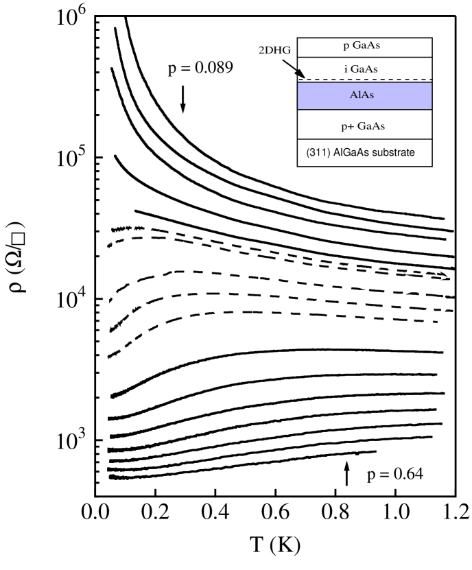
A metal-insulator transition similar to that seen in clean silicon MOSFETs has also been observed in other low-disordered, strongly-interacting 2D systems: -type SiGe heterostructures [11, 33], p-GaAs/AlGaAs heterostructures [12, 34, 35], n-GaAs/AlGaAs heterostructures [13, 36], AlAs heterostructures [14], and n-SiGe heterostructures [15, 16]. The values of the resistivity are quite similar in all systems. In Fig. 2, the resistivity is shown as a function of temperature for a -type GaAs/AlGaAs sample; here the interaction parameter, , changes between approximately 12 and 32.111These values were calculated assuming that the effective mass is independent of density and equal to , where is the free-electron mass. The main features are very similar to those found in silicon MOSFETs: when the resistivity at “high” temperatures exceeds the quantum resistance, (i.e., at hole densities below some critical value, ), the curves are insulating-like in the entire temperature range; for densities just above , the resistivity shows insulating-like behavior at higher temperatures and then drops by a factor of 2 to 3 at temperatures below a few hundred mK; and at yet higher hole densities, the resistivity is metallic in the entire temperature range. Note that the curves that separate metallic and insulating behavior have resistivities that increase with decreasing temperature at the higher temperatures shown; this is quite similar to the behavior of the separatrix in silicon MOSFETs when viewed over a broad temperature range (see Fig. 1). Below approximately 150 mK, the separatrix in -type GaAs/AlGaAs heterostructures is independent of temperature [12], as it is in Si MOSFETs below approximately 2 K. The resistivity of the separatrix in both systems extrapolates to or as , even though the corresponding carrier densities are very different.
2 THE EFFECT OF A MAGNETIC FIELD
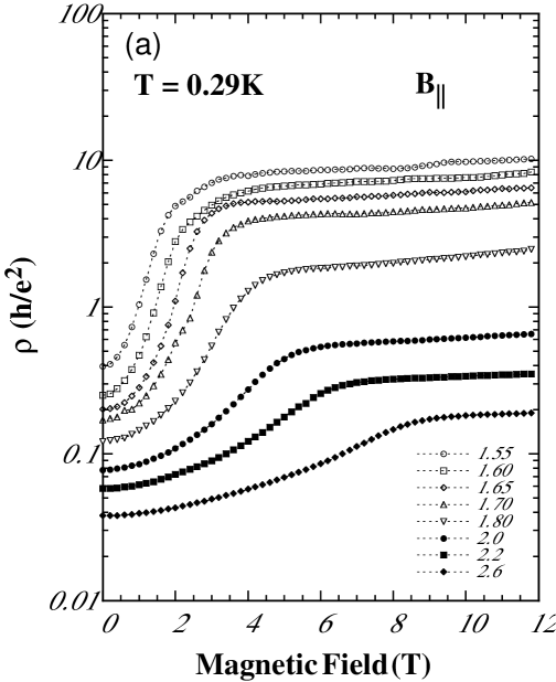
In ordinary metals, the application of a parallel magnetic field () does not lead to any dramatic changes in the transport properties: if the thickness of the 2D electron system is small compared to the magnetic length, the parallel field couples largely to the electrons’ spins while the orbital effects are suppressed. Only weak corrections to the conductivity are expected due to electron-electron interactions [38]. It therefore came as a surprise when Dolgopolov et al. [17] observed a dramatic suppression of the conductivity in dilute Si MOSFETs by a parallel in-plane magnetic field . The magnetoresistance in a parallel field was studied in detail by Simonian et al. [18] and Pudalov et al. [19], also in Si MOSFETs. In the left hand part of Fig. 3, the resistivity is shown as a function of parallel magnetic field at a fixed temperature of 0.3 K for several electron densities. The resistivity increases sharply as the magnetic field is raised, changing by a factor of about 4 at the highest density shown and by more than an order of magnitude at the lowest density, and then saturates and remains approximately constant up to the highest measuring field, tesla. The magnetic field where the saturation occurs, , depends on , varying from about 2 tesla at the lowest measured density to about 9 tesla at the highest. The metallic conductivity is suppressed in a similar way by magnetic fields applied at any angle relative to the 2D plane [39] independently of the relative directions of the measuring current and magnetic field [18, 40]. All these observations suggest that the giant magnetoresistance is due to coupling of the magnetic field to the electrons’ spins. Indeed, from an analysis of the positions of Shubnikov-de Haas oscillations in tilted magnetic fields [21, 41, 42] it was concluded that in MOSFETs, the magnetic field is equal to that required to fully polarize the electrons’ spins.
In -type GaAs/AlGaAs heterostructures, the effect of a parallel magnetic field is qualitatively similar, as shown in the right hand part of Fig. 3. As in the case of Si MOSFETs, there is a distinct knee that serves as a demarcation between the behavior in low and high fields. For high hole densities, Shubnikov-de Haas measurements [43] have shown that this knee is associated with full polarization of the spins by the in-plane magnetic field. However, unlike Si MOSFETs, the magnetoresistance in p-GaAs/AlGaAs heterostructures has been found to depend on the relative directions of the measuring current, magnetic field, and crystal orientation [44]; one should note that the crystal anisotropy of this material introduces added complications. In p-SiGe heterostructures, the parallel field was found to induce negligible magnetoresistance [33] because in this system the parallel field cannot couple to the spins due to very strong spin-orbit interactions.
Over and above the very large magnetoresistance induced by an in-plane magnetic fields, an even more important effect of a parallel field is that it causes the zero-field 2D metal to become an insulator [18, 45, 46, 47, 48]. The extreme sensitivity to parallel field is illustrated in Fig. 4. The top two panels compare the temperature dependence of the resistivity in the absence and in the presence of a parallel magnetic field. For , the resistivity displays the familiar, nearly symmetric (at temperatures above 0.2 K) critical behavior about the separatrix (the dashed line). However, in a parallel magnetic field of tesla, which is high enough to cause full spin polarization at this electron density, all the curves display “insulating-like” behavior, including those which start below at high temperatures. There is no temperature-independent separatrix at any electron density in a spin-polarized electron system [18, 46]. The effect of a parallel magnetic field is further demonstrated in the bottom panel of Fig. 4, where the slope of the resistivity calculated for the temperature interval K to K is plotted as a function of magnetic field at a fixed density; these data show explicitly and quantitatively that a magnetic field applied parallel to the plane of the electrons reduces the temperature dependence of the conductivity to near zero. Moreover, this was shown to be true over a broad range of electron densities extending deep into the metallic regime where the high-field conductivity is on the order of . The clear difference in behavior with and without in-plane magnetic field convincingly demonstrates that the spin-polarized and unpolarized states behave very differently and rules out explanations that predict similar behavior of the resistance regardless of the degree of spin polarization.
figure=fig4.eps
figure=fig4c.eps,width=2.3in
3 SPIN SUSCEPTIBILITY NEAR THE METAL-INSULATOR TRANSITION
1 Experimental measurements of the spin susceptibility
In Fermi-liquid theory, the electron effective mass and the -factor (and, therefore, the spin susceptibility, ) are renormalized due to electron-electron interactions [49]. Earlier experiments [50, 51], performed at relatively small values of to 5, confirmed the expected increase of the spin susceptibility. More recently, Okamoto et al.[21] observed a renormalization of by a factor of at up to about 6. At yet lower electron densities, in the vicinity of the metal-insulator transition, Kravchenko et al.[22] have observed a disappearance of the energy gaps at “cyclotron” filling factors which they interpreted as evidence for an increase of the spin susceptibility by a factor of at least five.
It was noted many years ago by Stoner that strong interactions can drive an electron system toward a ferromagnetic instability [31]. Within some theories of strongly interacting 2D systems [2, 52, 3, 4, 32], a tendency toward ferromagnetism is expected to accompany metallic behavior. The easiest way to estimate the spin magnetization of 2D electrons (or holes) is to measure the magnetic field above which the magnetoresistance saturates (and thus full spin polarization is reached) as a function of electron density. For non-interacting electrons, the saturation field is proportional to the electron density:
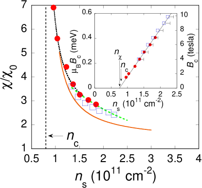
Here is the Landé -factor, is the effective mass, and is the Bohr magneton. Experiments [23, 24] have shown, however, that in strongly correlated 2D systems in Si MOSFETs, the parallel field required for full spin polarization extrapolates to zero at a non-zero electron density, . The left-hand panel of Fig.5 shows that the field for full polarization obtained by Shashkin et al.[23] extrapolates to zero at a finite electron density; the dashed line indicates the calculated for comparison; the fact that the measured lies significantly lower than the calculated value indicates that either or (or both) are larger than their band values. Using a different method of analysis, Vitkalov et al.[24] obtained a characteristic energy associated with the magnetic field dependence of the conductivity plotted as a function of electron density, as shown in the right-hand panel of Fig.5; the parameter decreases with decreasing density, and extrapolates to zero at a critical density labeled . That and , both measures of the field required to obtain complete spin polarization, extrapolate to zero at a finite density implies there is a spontaneous spin polarization at . Many Si MOSFET samples of different quality have been tested, and the results indicate that cm2 is independent of disorder. In the highest quality samples, was found to be within a few percent of the critical density for the metal-insulator transition, (but consistently below).
figure=fig5a.eps,width=2.45in \figsubcapa
figure=fig5b.eps,width=2.3in \figsubcapb
It is easy to recalculate the renormalized spin susceptibility using the data for :
where is the “non-interacting” value of the spin susceptibility. Such critical behavior of a thermodynamic parameter usually indicates that a system is approaching a phase transition, possibly of magnetic origin. However, direct evidence of a phase transition can only be obtained from measurements of thermodynamic properties. Given the tiny number of electrons in a dilute 2D layer, magnetic measurements are very hard to perform. A clever technique was designed and implemented by Prus et al.[53] and Shashkin et al. [54]. These authors modulated the parallel magnetic field with a small ac field, , and measured the tiny induced current between the gate and the two-dimensional electron system. The imaginary (out-of-phase) component of the current is proportional to , where is the chemical potential of the 2D gas. By applying the Maxwell relation , one can obtain the magnetization from the measured current. Full spin polarization corresponds to . Yet another way of finding the density for complete spin polarization is related to measurements of the thermodynamic density of states of the 2D system obtained from measurements[54] of the capacitance of a MOSFET: the thermodynamic density of states was found to change abruptly with the onset of complete spin polarization of the electrons’ spins.
The results obtained for the spin susceptibility are shown in Fig.6. One can see that upon approaching to the critical density of the metal-insulator transition, the spin susceptibility increases by almost an order of magnitude relative to its “non-interacting” value. This implies the occurrence of a spontaneous spin polarization (either Wigner crystal or ferromagnetic liquid) at low , although in currently available samples, the formation of a band tail of localized electrons at conceals the origin of the low-density phase. In other words, so far, one can only reach an incipient transition to a new phase.
A strong dependence of the magnetization on has also been seen [28, 55, 56] in other types of devices for near the critical density for the metal-insulator transition.
2 Effective mass or -factor?
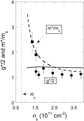
In principle, the strong increase of the Pauli spin susceptibility at low electron densities can be due to either the increase of the effective mass or the Lande -factor (or both). The effective mass was measured by several groups employing different methods [25, 29, 30] which gave quantitatively similar results. The values and as a function of the electron density are shown in Fig. 7 (here is the factor in bulk silicon, is the band mass equal to , and is the free electron mass). In the high region (relatively weak interactions), the enhancement of both and is relatively small, with both values increasing slightly with decreasing electron density, in agreement with earlier data [58]. Also, the renormalization of the factor is dominant compared to that of the effective mass, consistent with theoretical studies [59, 60, 61].
In contrast, the renormalization at low (near the critical region), where , is striking. As the electron density is decreased, the effective mass increases dramatically while the factor remains essentially constant and relatively small, . Hence, it is the effective mass, rather than the factor, that is responsible for the drastically enhanced spin susceptibility near the metal-insulator transition.
3 Effective mass as a function of
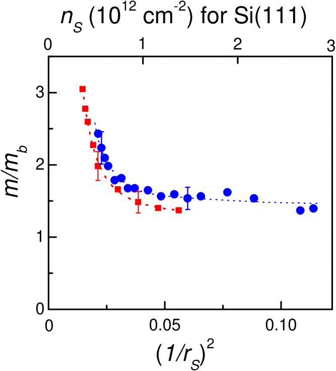
The effective mass has also been measured in a dilute 2D electron system in (111)-silicon. This system is interesting because the band electron mass is approximately a factor of two larger than it is in (100)-silicon. In addition, the (111)-silicon samples used in these experiments have a much higher level of disorder. Remarkably, the relative enhancement of the effective mass, i.e., , was found to be essentially the same function of the interaction parameter, , as in (100) samples of Si MOSFETs. Shown in Fig. 8, the effective mass plotted in units as a function of is essentially the same for the two systems within the experimental uncertainty, despite the fact that the band mass differs by about a factor of two and the level disorder differs by almost one order of magnitude. This implies that the relative mass enhancement is determined solely by the strength of the electron-electron interactions.
4 Comparison with theory and open questions
Many theories have been proposed to account for the experimental observations summarized above. These include exotic superconductivity,[63] the formation of a disordered Wigner solid,[64] microemulsion phases,[65, 66, 67] percolation,[68] and a non-Fermi liquid state [69]. In what follows, we restrict our discussion to theories that provide numerical predictions with which experimental can be compared directly.
1 Ballistic regime ()
When the resistivity of a sample is much smaller than , the electrons are in a ballistic regime for temperatures ; this encompasses most of the experimentally accessible range except in samples with electron densities that are very close to the critical density. Theories [70, 71, 72, 73, 74, 75, 76] that invoke the effect of electron screening attempt to explain the transport results in the ballistic regime by extrapolating classical formulas for the resistivity, valid for , to the regime where . Indeed, quantitatively successful comparisons with experiment have been reported.[72, 74, 75, 76] However, at large , the screening length obtained using a random-phase approximation becomes parametrically smaller than the spacing between electrons: [67]. Screening lengths smaller than the distance between electrons are clearly unphysical.
This approach was corrected by Zala et al.[77], who considered the contribution due to the scattering from the Friedel oscillations induced by impurities. At small , the “insulating-like” sign of is obtained, in agreement with experiments on samples with . However, when extrapolated to large enough , changes sign, and becomes a linearly increasing function of . This theory [77] predicts the complete suppression of the metallic behavior in parallel magnetic fields sufficiently strong to completely polarize spins, again in agreement with the experiments. However, one should keep in mind that this theory considers corrections to the conductivity that are small compared to the Drude conductivity. By contrast, changes in resistivity by an order of magnitude are often observed experimentally.
2 Scaling theory of the metal-insulator transition in 2D: diffusive regime ()
The two-parameter scaling theory [78, 32] of quantum diffusion in an interacting disordered system is based on the scaling hypothesis that both the resistivity and the electron-electron scattering amplitudes, , become scale (temperature) dependent. Essentially, this is the theory of Anderson localization in the presence of electron-electron interactions. The renormalization-group (RG) equations describing the evolution of the resistance and the scattering amplitude in 2D have the form [78]
| (1) | |||||
| (2) |
where , is the elastic scattering time, , and is the number of degenerate valleys in the spectrum. The resistance, , is a non-monotonic function of temperature, reaching a maximum value at some temperature with a metallic temperature dependence () for . Furthermore, can be written as
| (3) |
where is a universal function shown by the solid curve in Fig. 9(a). The strength of spin-dependent interactions, , is also a universal function of , shown by the solid line in Fig. 9(b).
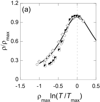
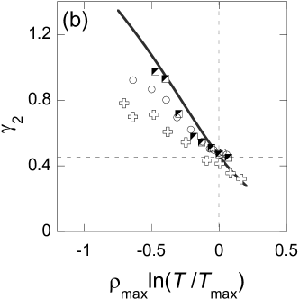
This theory can account for the large changes in resistivity observed experimentally, and provides quantitative functions that can be directly compared with the experimental data. Such a comparison was made by Anissimova et al.,[79] who deduced the interaction amplitude from the magnetoresistance; the results are presented in Figs. 9(a) and (b). The agreement between theory and experiment is especially striking given that the theory has no adjustable parameters. Systematic deviations from the universal curves occur at lower densities as higher order corrections in become important. Furthermore, the resistivity reaches a maximum at , in excellent agreement with theory [78] for .
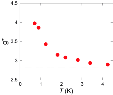
The data for enables one to calculate the renormalized Landé g-factor . As shown in Fig.10, at cm-2, the Landé g-factor increases from at the highest temperature to at the lowest. Therefore, the g-factor becomes temperature-dependent in the diffusive regime and increases with decreasing temperature, in agreement with the predictions of Punnoose and Finkelshtein[78, 32]. Note that at higher temperatures it is close to the temperature-independent “ballistic” value of about 2.8.
However, it should be noted that a theory based on electron interference effects can predict substantial changes of resistivity only in the near vicinity of the critical point, where . At much lower resistivities , only small logarithmic corrections are possible, while the experiments demonstrate very large changes in resistivity even deep in the metallic region. Therefore, although the theory of Punnoose and Finkelstein [78, 32] quantitatively describes experimental data in the close vicinity of the transition, it cannot explain the large effects observed far from the transition. It should be further noted that most of the experiments in GaAs- and n-SiGe-based devices are performed in the ballistic regime where this theory is irrelevant. Given the conspicuous similarity of the results obtained on different 2D systems, whether diffusive or ballistic, it seems clear that a unified theory applicable in both regimes is needed to account for the transport data.
Such a theory, based on the Pomeranchuk effect, was proposed by Spivak and Kivelson [65, 66, 67]. In essence, this theory proposes that when the interaction energy is much higher than the Fermi energy, the short-range interactions are of the Wigner-crystalline type. As the temperature or magnetic field is increased, the surface fraction occupied by the Wigner crystallites grows, explaining the metallic temperature dependence of the resistance and the giant positive magnetoresistance observed at low temperatures. Moreover, this theory predicts that the metallic temperature dependence of the resistance is quenched in magnetic fields strong enough to completely polarize the electrons’ spins. The Pomeranchuk effect provides a qualitative explanation of all the major experimental observations; however, a quantitative theory is not currently available.
3 Spin susceptibility and the effective mass enhancement
There are several mechanism that could lead to the strong enhancement of the effective mass at low carrier densities (high ). Within Fermi liquid theory, the enhancement of and is due to spin exchange effects. Extension of the Fermi liquid model to relatively large [59, 60, 61] is problematic, the main outcome being that the renormalization of is large compared to that of . In the limiting case of high , one may expect a divergence of the factor that corresponds to the Stoner instability. These predictions are in obvious contradiction to the experimental data. The divergence of the effective mass and spin susceptibility follow also from the Gutzwiller variational approach [81] (see also Ref.[82]). Recent theoretical developments include the following. Using a renormalization group analysis for multi-valley 2D systems, it has been found that the spin susceptibility increases dramatically as the density is decreased toward the critical density for the metal-insulator transition, while the factor remains nearly intact [32]. However, this prediction is made for the diffusive regime, , while the spin susceptibility enhancement has been observed well into the ballistic regime, . In the Fermi-liquid-based model of Khodel et al [83], a flattening at the Fermi energy in the spectrum that leads to a diverging effective mass has been predicted, in qualitative agreement with experiment, but a detailed microscopic theory is needed before conclusions can be drawn. The strong increase of the effective mass has also been obtained (in the absence of disorder) by solving an extended Hubbard model using dynamical mean-field theory [84, 85]. This is consistent with experiment, especially taking into account that the relative mass enhancement has been experimentally found to be independent of the level of the disorder [62].
5 Summary
Although the behavior in the close vicinity of the transition is quantitatively described by the renormalization-group theory of Punnoose and Finkelstein [32] without any fitting parameters, there is currently no microscopic theory that can explain the whole range of observed phenomena. The origin of the large changes in the resistance deep in the metallic phase remains unclear, with suggested explanations ranging from temperature-dependent screening [73, 72, 74, 75, 76] to an analog of the Pomeranchuk effect [65, 66, 67]. From an empirical perspective, numerous experiments on various strongly correlated 2D electron and hole systems strongly suggest the existence of a metal-insulator transition and a metallic phase in two-dimensions, despite the persistent view on the part of many that such a transition is impossible in 2D.
References
- 1. E. Abrahams, P. W. Anderson, D. C. Licciardello, and T. V. Ramakrishnan, Scaling theory of localization: Absence of quantum diffusion in two dimensions, Phys. Rev. Lett. 42, 673–676, (1979).
- 2. A. M. Finkel’shtein, Influence of Coulomb interaction on the properties of disordered metals, Sov. Phys. - JETP. 57, 97–108, (1983).
- 3. A. M. Finkel’shtein, Weak localization and Coulomb interaction in disordered-systems, Z. Phys. B. 56, 189–196, (1984).
- 4. C. Castellani, C. Di Castro, P. A. Lee, and M. Ma, Interaction-driven metal-insulator transitions in disordered fermion systems, Phys. Rev. B. 30, 527–543, (1984).
- 5. T. N. Zavaritskaya and E. I. Zavaritskaya, Metal-insulator transition in inversion channels of silicon MOS structures, JETP Lett. 45, 609–613, (1987).
- 6. S. V. Kravchenko, G. V. Kravchenko, J. E. Furneaux, V. M. Pudalov, and M. D’Iorio, Possible metal-insulator-transition at in 2 dimensions, Phys. Rev. B. 50, 8039–8042, (1994).
- 7. S. V. Kravchenko, W. E. Mason, G. E. Bowker, J. E. Furneaux, V. M. Pudalov, and M. D’Iorio, Scaling of an anomalous metal-insulator-transition in a 2-dimensional system in silicon at , Phys. Rev. B. 51, 7038–7045, (1995).
- 8. S. V. Kravchenko, D. Simonian, M. P. Sarachik, W. Mason, and J. E. Furneaux, Electric field scaling at a metal-insulator transition in two dimensions, Phys. Rev. Lett. 77, 4938–4941, (1996).
- 9. D. Popović, A. B. Fowler, and S. Washburn, Metal-insulator transition in two dimensions: Effects of disorder and magnetic field, Phys. Rev. Lett. 79, 1543–1546, (1997).
- 10. R. N. McFarland, T. M. Kott, L. Sun, K. Eng, and B. E. Kane, Temperature-dependent transport in a sixfold degenerate two-dimensional electron system on a H-Si(111) surface, Phys. Rev. B. 80, 161310(R), (2009).
- 11. P. T. Coleridge, R. L. Williams, Y. Feng, and P. Zawadzki, Metal-insulator transition at in -type SiGe, Phys. Rev. B. 56, R12764–R12767, (1997).
- 12. Y. Hanein, U. Meirav, D. Shahar, C. C. Li, D. C. Tsui, and H. Shtrikman, The metalliclike conductivity of a two-dimensional hole system, Phys. Rev. Lett. 80, 1288–1291, (1998).
- 13. Y. Hanein, D. Shahar, J. Yoon, C. C. Li, D. C. Tsui, and H. Shtrikman, Observation of the metal-insulator transition in two-dimensional n-type GaAs, Phys. Rev. B. 58, R13338–R13340, (1998).
- 14. S. J. Papadakis and M. Shayegan, Apparent metallic behavior at of a two-dimensional electron system in AlAs, Phys. Rev. B. 57, R15068–R15071, (1998).
- 15. T. Okamoto, M. Ooya, K. Hosoya, and S. Kawaji, Spin polarization and metallic behavior in a silicon two-dimensional electron system, Phys. Rev. B. 69, 041202(R), (2004).
- 16. K. Lai, W. Pan, D. C. Tsui, S. A. Lyon, M. Muhlberger, and F. Schäffler, Two-dimensional metal-insulator transition and in-plane magnetoresistance in a high-mobility strained Si quantum well, Phys. Rev. B. 72, 081313(R), (2005).
- 17. V. T. Dolgopolov, G. V. Kravchenko, A. A. Shashkin, and S. V. Kravchenko, Properties of electron insulating phase in Si inversion-layers at low-temperatures, JETP Lett. 55, 733–737, (1992).
- 18. D. Simonian, S. V. Kravchenko, M. P. Sarachik, and V. M. Pudalov, Magnetic field suppression of the conducting phase in two dimensions, Phys. Rev. Lett. 79, 2304–2307, (1997).
- 19. V. M. Pudalov, G. Brunthaler, A. Prinz, and G. Bauer, Instability of the two-dimensional metallic phase to a parallel magnetic field, JETP Lett. 65, 932–937, (1997).
- 20. M. Y. Simmons, A. R. Hamilton, M. Pepper, E. H. Linfield, P. D. Rose, D. A. Ritchie, A. K. Savchenko, and T. G. Griffiths, Metal-insulator transition at in a dilute two dimensional GaAs-AlGaAs hole gas, Phys. Rev. Lett. 80, 1292–1295, (1998).
- 21. T. Okamoto, K. Hosoya, S. Kawaji, and A. Yagi, Spin degree of freedom in a two-dimensional electron liquid, Phys. Rev. Lett. 82, 3875–3878, (1999).
- 22. S. V. Kravchenko, A. A. Shashkin, D. A. Bloore, and T. M. Klapwijk, Shubnikov-de Haas oscillations near the metal-insulator transition in a two-dimensional electron system in silicon, Solid State Commun. 116, 495–499, (2000).
- 23. A. A. Shashkin, S. V. Kravchenko, V. T. Dolgopolov, and T. M. Klapwijk, Indication of the ferromagnetic instability in a dilute two-dimensional electron system, Phys. Rev. Lett. 87, 086801, (2001).
- 24. S. A. Vitkalov, H. Zheng, K. M. Mertes, M. P. Sarachik, and T. M. Klapwijk, Scaling of the magnetoconductivity of silicon MOSFETs: Evidence for a quantum phase transition in two dimensions, Phys. Rev. Lett. 87, 086401, (2001).
- 25. A. A. Shashkin, S. V. Kravchenko, V. T. Dolgopolov, and T. M. Klapwijk, Sharp increase of the effective mass near the critical density in a metallic two-dimensional electron system, Phys. Rev. B. 66, 073303, (2002).
- 26. S. A. Vitkalov, M. P. Sarachik, and T. M. Klapwijk, Spin polarization of strongly interacting two-dimensional electrons: The role of disorder, Phys. Rev. B. 65, 201106(R), (2002).
- 27. V. M. Pudalov, M. E. Gershenson, H. Kojima, N. Butch, E. M. Dizhur, G. Brunthaler, A. Prinz, and G. Bauer, Low-density spin susceptibility and effective mass of mobile electrons in Si inversion layers, Phys. Rev. Lett. 88, 196404, (2002).
- 28. J. Zhu, H. L. Stormer, L. N. Pfeiffer, K. W. Baldwin, and K. W. West, Spin susceptibility of an ultra-low-density two-dimensional electron system, Phys. Rev. Lett. 90, 056805, (2003).
- 29. A. A. Shashkin, M. Rahimi, S. Anissimova, S. V. Kravchenko, V. T. Dolgopolov, and T. M. Klapwijk, Spin-independent origin of the strongly enhanced effective mass in a dilute 2D electron system, Phys. Rev. Lett. 91, 046403, (2003).
- 30. S. Anissimova, A. Venkatesan, A. A. Shashkin, M. R. Sakr, S. V. Kravchenko, and T. M. Klapwijk, Magnetization of a strongly interacting two-dimensional electron system in perpendicular magnetic fields, Phys. Rev. Lett. 96, 046409, (2006).
- 31. E. C. Stoner, Ferromagnetism, Rep. Prog. Phys. 11, 43–112, (1946).
- 32. A. Punnoose and A. M. Finkel’stein, Metal-insulator transition in disordered two-dimensional electron systems, Science. 310, 289–291, (2005).
- 33. V. Senz, U. Dötsch, U. Gennser, T. Ihn, T. Heinzel, K. Ensslin, R. Hartmann, and D. Grützmacher, Metal-insulator transition in a 2-dimensional system with an easy spin axis, Ann. Phys. (Leipzig). 8, 237–240, (1999).
- 34. J. Yoon, C. C. Li, D. Shahar, D. C. Tsui, and M. Shayegan, Wigner crystallization and metal-insulator transition of two-dimensional holes in GaAs at , Phys. Rev. Lett. 82, 1744–1747, (1999).
- 35. A. P. Mills, Jr., A. P. Ramirez, L. N. Pfeiffer, and K. W. West, Nonmonotonic temperature-dependent resistance in low density 2D hole gases, Phys. Rev. Lett. 83, 2805–2808, (1999).
- 36. M. P. Lilly, J. L. Reno, J. A. Simmons, I. B. Spielman, J. P. Eisenstein, L. N. Pfeiffer, K. W. West, E. H. Hwang, and S. Das Sarma, Resistivity of dilute 2D electrons in an undoped GaAs heterostructure, Phys. Rev. Lett. 90, 056806, (2003).
- 37. X. P. A. Gao, G. S. Boebinger, A. P. Mills, Jr., A. P. Ramirez, L. N. Pfeiffer, and K. W. West, Spin-polarization-induced tenfold magnetoresistivity of highly metallic two-dimensional holes in a narrow GaAs quantum well, Phys. Rev. B. 73, 241315(R), (2006).
- 38. P. A. Lee and T. V. Ramakrishnan, Disordered electronic systems, Rev. Mod. Phys. 57, 287–337, (1985).
- 39. S. V. Kravchenko, D. Simonian, M. P. Sarachik, A. D. Kent, and V. M. Pudalov, Effect of tilted magnetic field on the anomalous H=0 conducting phase in high-mobility Si MOSFETs, Phys. Rev. B. 58, 3553–3556, (1998).
- 40. V. M. Pudalov, G. Brunthaler, A. Prinz, and G. Bauer, Weak anisotropy and disorder dependence of the in-plane magnetoresistance in high-mobility (100) Si-inversion layers, Phys. Rev. Lett. 88, 076401, (2002).
- 41. S. A. Vitkalov, H. Zheng, K. M. Mertes, M. P. Sarachik, and T. M. Klapwijk, Small-angle Shubnikov-de Haas measurements in a 2D electron system: The effect of a strong in-plane magnetic field, Phys. Rev. Lett. 85, 2164–2167, (2000).
- 42. S. A. Vitkalov, M. P. Sarachik, and T. M. Klapwijk, Spin polarization of two-dimensional electrons determined from Shubnikov-de Haas oscillations as a function of angle, Phys. Rev. B. 64, 073101, (2001).
- 43. E. Tutuc, E. P. De Poortere, S. J. Papadakis, and M. Shayegan, In-plane magnetic field-induced spin polarization and transition to insulating behavior in two-dimensional hole systems, Phys. Rev. Lett. 86, 2858–2861, (2001).
- 44. S. J. Papadakis, E. P. De Poortere, M. Shayegan, and R. Winkler, Anisotropic magnetoresistance of two-dimensional holes in GaAs, Phys. Rev. Lett. 84, 5592–5595, (2000).
- 45. K. M. Mertes, H. Zheng, S. A. Vitkalov, M. P. Sarachik, and T. M. Klapwijk, Temperature dependence of the resistivity of a dilute two-dimensional electron system in high parallel magnetic field, Phys. Rev. B. 63, 041101(R), (2001).
- 46. A. A. Shashkin, S. V. Kravchenko, and T. M. Klapwijk, Metal-insulator transition in 2D: equivalence of two approaches for determining the critical point, Phys. Rev. Lett. 87, 266402, (2001).
- 47. X. P. A. Gao, A. P. Mills, Jr., A. P. Ramirez, L. N. Pfeiffer, and K. W. West, Weak-localization-like temperature-dependent conductivity of a dilute two-dimensional hole gas in a parallel magnetic field, Phys. Rev. Lett. 88, 166803, (2002).
- 48. Y. Tsui, S. A. Vitkalov, M. P. Sarachik, and T. M. Klapwijk, Conductivity of silicon inversion layers: Comparison with and without an in-plane magnetic field, Phys. Rev. B. 71, 13308, (2005).
- 49. L. D. Landau, The theory of a Fermi liquid, Sov. Phys. - JETP. 3, 920–925, (1957).
- 50. F. F. Fang and P. J. Stiles, Effects of a tilted magnetic field on a two-dimensional electron gas, Phys. Rev. 174, 823–828, (1968).
- 51. J. L. Smith and P. J. Stiles, Electron-electron interactions continuously variable in the range , Phys. Rev. Lett. 29, 102–104, (1972).
- 52. A. M. Finkel’shtein, Spin fluctuations in disordered systems near the metal-insulator transition, JETP Lett. 40, 796–799, (1984).
- 53. O. Prus, Y. Yaish, M. Reznikov, U. Sivan, and V. M. Pudalov, Thermodynamic spin magnetization of strongly correlated two-dimensional electrons in a silicon inversion layer, Phys. Rev. B. 67, 205407, (2003).
- 54. A. A. Shashkin, S. Anissimova, M. R. Sakr, S. V. Kravchenko, V. T. Dolgopolov, and T. M. Klapwijk, Pauli spin susceptibility of a strongly correlated 2D electron liquid, Phys. Rev. Lett. 96, 036403, (2006).
- 55. K. Vakili, Y. P. Shkolnikov, E. Tutuc, E. P. De Poortere, and M. Shayegan, Spin susceptibility of two-dimensional electrons in narrow AlAs quantum wells, Phys. Rev. Lett. 92, 226401, (2004).
- 56. T. M. Lu, L. Sun, D. C. Tsui, S. Lyon, W. Pan, M. Muhlberger, F. Schäffler, J. Liu, and Y. H. Xie, In-plane field magnetoresistivity of Si two-dimensional electron gas in Si/SiGe quantum wells at 20 mK, Phys. Rev. B. 78, 233309, (2008).
- 57. A. A. Shashkin, S. V. Kravchenko, and T. M. Klapwijk, Metal-insulator transition in 2D: equivalence of two approaches for determining the critical point, Phys. Rev. Lett. 87, 266402, (2001).
- 58. T. Ando, A. B. Fowler, and F. Stern, Electronic-properties of two-dimensional systems, Rev. Mod. Phys. 54, 437–672, (1982).
- 59. N. Iwamoto, Static local-field corrections of two-dimensional electron liquids, Phys. Rev. B. 43, 2174–2182, (1991).
- 60. Y. Kwon, D. M. Ceperley, and R. M. Martin, Quantum Monte Carlo calculation of the Fermi-liquid parameters in the two-dimensional electron gas, Phys. Rev. B. 50, 1684–1694, (1994).
- 61. G.-H. Chen and M. E. Raikh, Exchange-induced enhancement of spin-orbit coupling in two-dimensional electronic systems, Phys. Rev. B. 60, 4826–4833, (1999).
- 62. A. A. Shashkin, A. A. Kapustin, E. V. Deviatov, V. T. Dolgopolov, and Z. D. Kvon, Strongly enhanced effective mass in dilute two-dimensional electron systems: System-independent origin, Phys. Rev. B. 76, 241302(R), (2007).
- 63. P. Phillips, Y. Wan, I. Martin, S. Knysh, and D. Dalidovich, Superconductivity in a two-dimensional electron gas, Nature (London). 395, 253–257, (1998).
- 64. S. Chakravarty, S. Kivelson, C. Nayak, and K. Voelker, Wigner glass, spin-liquids, and the metal-insulator transition, Phil. Mag. B. 79, 859–868, (1999).
- 65. B. Spivak, Phase separation in the two-dimensional electron liquid in MOSFETs, Phys. Rev. B. 67, 125205, (2003).
- 66. B. Spivak and S. A. Kivelson, Intermediate phases of the two dimensional electron fluid between the Fermi liquid and the Wigner crystal, Phys. Rev. B. 70, 155114, (2004).
- 67. B. Spivak and S. A. Kivelson, Transport in two dimensional electronic micro-emulsions, Ann. Phys. 321, 2071–2115, (2006).
- 68. Y. Meir, Percolation-type description of the metal-insulator transition in two dimensions, Phys. Rev. Lett. 83, 3506–3509, (1999).
- 69. S. Chakravarty, L. Yin, and E. Abrahams, Interactions and scaling in a disordered two-dimensional metal, Phys. Rev. B. 58, R559–R562, (1998).
- 70. F. Stern, Calculated temperature dependence of mobility in silicon inversion layers, Phys. Rev. Lett. 44, 1469–1472, (1980).
- 71. A. Gold and V. T. Dolgopolov, Temperature dependence of the conductivity for the two-dimensional electron gas: Analytical results for low temperatures, Phys. Rev. B. 33, 1076–1084, (1986).
- 72. S. Das Sarma and E. H. Hwang, Charged impurity scattering limited low temperature resistivity of low density silicon inversion layers, Phys. Rev. Lett. 83, 164–167, (1999).
- 73. V. T. Dolgopolov and A. Gold, Magnetoresistance of a two-dimensional electron gas in a parallel magnetic field, JETP Lett. 71, 27–30, (2000).
- 74. S. Das Sarma and E. H. Hwang, Parallel magnetic field induced giant magnetoresistance in low density quasi-two-dimensional layers, Phys. Rev. B. 61, R7838–R7841, (2000).
- 75. S. Das Sarma and E. H. Hwang, Low density finite temperature apparent insulating phase in 2D semiconductor systems, Phys. Rev. B. 68, 195315, (2003).
- 76. S. Das Sarma and E. H. Hwang, Metallicity and its low temperature behavior in dilute 2D carrier systems, Phys. Rev. B. 69, 195305, (2004).
- 77. G. Zala, B. N. Narozhny, and I. L. Aleiner, Interaction corrections at intermediate temperatures: Longitudinal conductivity and kinetic equation, Phys. Rev. B. 64, 214204, (2001).
- 78. A. Punnoose and A. M. Finkelstein, Dilute electron gas near the metal-insulator transition: Role of valleys in silicon inversion layers, Phys. Rev. Lett. 88, 016802, (2001).
- 79. S. Anissimova, S. V. Kravchenko, A. Punnoose, A. M. Finkel’stein, and T. M. Klapwijk, Flow diagram of the metal-insulator transition in two dimensions, Nature Phys. 3, 707–710, (2007).
- 80. A. Mokashi and S. V. Kravchenko, unpublished. (2009).
- 81. W. F. Brinkman and T. M. Rice, Application of Gutzwiller’s variational method to the metal-insulator transition, Phys. Rev. B. 2, 4302–4304, (1970).
- 82. V. T. Dolgopolov, On effective electron mass of silicon field structures at low electron densities, JETP Lett. 76, 377–379, (2002).
- 83. V. A. Khodel, J. W. Clark, and M. V. Zverev, Thermodynamic properties of Fermi systems with flat single-particle spectra, Europhys. Lett. 72, 256–262, (2005).
- 84. S. Pankov and V. Dobrosavljević, Self-doping instability of the Wigner-Mott insulator, Phys. Rev. B. 77, 085104, (2008).
- 85. A. Camjayi, K. Haule, V. Dobrosavljević, and G. Kotliar, Coulomb correlations and the Wigner—-Mott transition, Nature Phys. 4, 932–935, (2008).