Magneto-transport through graphene nano-ribbons
Abstract
We investigate magneto-transport through graphene nano-ribbons as a function of gate and bias voltage, and temperature. We find that a magnetic field systematically leads to an increase of the conductance on a scale of a few tesla. This phenomenon is accompanied by a decrease in the energy scales associated to charging effects, and to hopping processes probed by temperature-dependent measurements. All the observations can be interpreted consistently in terms of strong-localization effects caused by the large disorder present, and exclude that the insulating state observed in nano-ribbons can be explained solely in terms of a true gap between valence and conduction band.
pacs:
85.35.-p, 73.23.-b, 72.80.Vp, 73.20.FzSingle-layer graphene is a zero-gap semiconductor, whose valence and conduction bands touch at two inequivalent points (the K and K’ points) at the edge of the first Brillouin zone Gei . Owing to the absence of a band-gap, the conductance of graphene remains finite irrespective of the position of the chemical potential. The impossibility to turn off the conductivity hinders the fabrication of high-quality field-effect transistors, and poses problems for the use of graphene in electronic devices. A possible solution is the use of graphene nano-ribbons, in which the opening of a gap between valence and conduction band has been predicted theoretically Gap-th .
According to theory, a gap in nano-ribbons should open as a consequence of size quantization and, depending on the specific case considered, interaction effects Gap-th . Transport experiments indeed find that the conductance through narrow ribbons is very strongly suppressed when the Fermi energy is close to the charge neutrality point Kim-Gap ; Gap-exp . However, it is unclear whether the opening of a band-gap is the correct explanation for the experimental observations. On the one hand, a gap would lead to a conductance suppression similar to what is found experimentally, with characteristic energy scales (as probed in temperature- and bias-dependent measurements) comparable to the observed ones Kim-Gap . On the other hand, the theoretical predictions rely on edge structures that are ideal on the atomic scale, whereas this is certainly not the case in real devices. This is why many theoretical studies have analyzed the role of strong localization of electron wave-functions –possibly in combination with charging effects– as the origin of the conductance suppression observed in the experiments on nano-ribbons SL-th .
Existing studies of transport through graphene nano-ribbons have mainly relied on measurements of conductance as a function of carrier density and temperature, and have not led to a definite conclusion as to the nature of the transport gap. Here, we present a systematic investigation focusing on the magneto-transport properties. We show that, in the transport gap, the application of magnetic field always leads to a conductance increase, together with a decrease in the characteristic energy scale associated to the conductance suppression. We perform an analysis of these measurements that excludes the opening of a band-gap as the sole explanation for the observed insulating behavior, and accounts for all our observations (including the gate-voltage and temperature dependence) in a consistent way, in terms of strong-localization effects caused by the larger disorder present in narrow ribbon geometries.
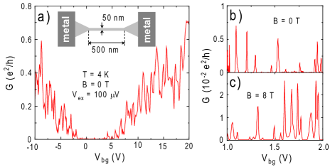
We have investigated many devices consisting of graphene nano-ribbons fabricated using the by-now conventional exfoliation procedure. The details of the device fabrication process and ribbon patterning (based on etching in an Ar plasma) are identical to those that we have used for the realization of Aharonov-Bohm rings (see AB ). The device geometry is schematically shown in the inset of Fig. 1(a). Different dimensions were used, with the ribbon width varying approximately between 50 and 100 nm, and the ribbon length between 500 and 1000 nm. The region where the metal electrodes contact the graphene layer is intentionally kept large, to exclude effects due to the contact resistance. Conductance measurements on many different devices yielding consistent results were performed in a two-terminal configuration as a function of back-gate voltage, temperature, and magnetic field. Unless stated otherwise, here we show data obtained from one of these ribbons (with length nm and width nm), representative of the overall behaviour observed.
Fig. 1(a) shows the linear conductance of the ribbon as a function of gate voltage. The conductance is strongly suppressed in the voltage range , that we refer to as the transport gap (the transport gap depends weakly on the ribbon length and it is larger for longer devices, consistently with the results of Ref. Kim-SL ). Fig. 1(b) zooms-in on this range, showing conductance peaks at several gate voltages (with the conductance vanishing elsewhere) originating from charging effects. Measurements as a function of gate () and bias () voltage show that the conductance is highly suppressed at low (Fig. 2(a)), and exhibit characteristic ”diamond-like” structures (Fig. 3(a)) typical of Coulomb blockade. These results are similar to others already reported Kim-Gap ; Gap-exp , and clearly indicate that the electrons are confined in small regions of the ribbon –which we call islands– whose area is sufficiently small to have a significant charging energy. Fig. 3(a) shows that the diamonds are irregular and partially overlap, indicating that the islands in the ribbon vary in size, and that electrons have to propagate through several of them while traversing the ribbon. At a microscopic level, the question is what is the mechanism that determines the presence of the islands, i.e. the presence of a band-gap or the effect of strong localization.
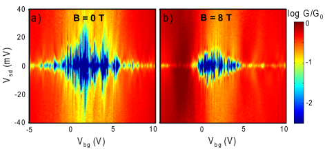
The analysis of the influence of magnetic field provide additional important information. In Fig. 2 (a) and (b), the conductance measured as a function of gate and bias voltage at 0 T and 8 T can be directly compared. The bias and gate voltage ranges where the conductance is suppressed are significantly smaller when a high magnetic field is applied. Also the Coulomb peaks and diamonds are affected (compare Fig. 1(b) and (c), and Fig. 3(a) and (b)): in the presence of a high magnetic field, the average number of Coulomb peaks in a given gate voltage range is larger, and the average peak conductance is higher. Qualitatively, these observations indicate that the average island size increases when a magnetic field field is applied, since for larger islands the charging energy is smaller.
The continuous evolution from T to 8 T is shown in Fig. 4(a). In Fig. 4(b) we show the average (over gate voltage varying in the transport gap) of the conductance as a function of magnetic field. Since the conductance between the Coulomb peaks is negligibly small, this quantity measures the average peak conductance and the number of peaks present. Fig. 4(b) shows the average conductance for the sample that we are discussing, and for two other nano-ribbons having width nm and nm. We see that the average conductance increases with magnetic field for T and that it saturates for T. We conclude that the average number of Coulomb peaks and the peak conductance increase for T, but remains approximately constant for T. Unexpectedly, the average conductance saturates at approximately similar values of the magnetic field in the different devices, irrespective of the ribbon width.
In order to analyze the results of the magneto-transport experiments, we first go back to the data shown in Fig. 1(a), and look at a larger gate voltage range (outside the transport gap), to estimate the value of the electron mean-free path. From the average slope (i.e., neglecting the fluctuations) of the conductance versus gate voltage, , measured at high charge density (where the conductance is much larger than in the transport gap), we determine the field-effect mobility cm2/Vs. This value is smaller than the typical values usually found for large graphene flakes on SiO2 substrates ( cm2/Vs Gei ), confirming that graphene nanoribbons are more disordered note1 . We determine using the Einstein relation , where is the diffusion constant and the density of states (, with and the Fermi energy and velocity, respectively). From the conductivity, measured at V, and determining from the charge density induced electrostatically cm-2, we obtain m2/s. The corresponding electron mean-free path is then obtained from nm, smaller than the ribbon width ( nm).

The short mean-free path values are indicative of strong disorder, and suggest that a scenario based on strong-localization may be appropriate (consistently with the conclusion reported recently in Ref. Kim-SL , and theoretical predictions SL-th ). A signature of strong localization is a positive magneto-conductance, originating from an increase of the localization length due to time reversal symmetry breaking Books ; Ger . In the strong localization regime, time reversal symmetry is broken when the magnetic flux through an area corresponding to the square of the localization length is of the order of the flux quantum . This mechanism can explain our data of Fig. 4(b), which show that the average conductance at low does indeed increase when the magnetic field is increased from 0 T to 3 T, and provide an estimate of the localization length of nm. This value of is somewhat smaller than (but comparable with) the width of the three ribbons whose data are plotted in Fig. 4(b): this is why the magneto-conductance saturates at approximately the same magnetic field in the different devices. Further, we estimate the phase coherence length by using the value of the diffusion constant obtained above and the phase coherence time ps reported in Ref. Sav . We obtain nm, from which we conclude that , the correct hierarchy of length scales for the strong localization regime Books . Note also that at low charge density, where the number of transverse channels occupied is small, and , as expected from theory Books . The increase in conductance observed at higher charge density can then be attributed to an increase in localization length, due to the increase in the number of occupied transverse channels.

It is particularly important to discuss whether the observed positive magneto-conductance can be understood if the formation of islands in the ribbons is due to the opening of a band-gap (and not by strong-localization effects). In the presence of a high magnetic field, well-defined Landau levels are expected to appear in the energy spectrum when the magnetic length, becomes sufficiently smaller than the ribbon width (when , the finite width does not affect the Landau levels). Owing to the presence of a zero-energy Landau level in graphene QHE , a large magnetic field should cause the closing of the gap and lead to the appearance of edge states that would contribute to the conductance (). This mechanism could explain a positive magneto-conductance. In the experiments, however, we do not observe any signature of the formation of edge states –the low-temperature conductance in the transport gap remains always much smaller than – despite the fact that 10 nm for 8 T (ten time smaller than the largest ribbon that we discuss here). This observation again implies that ribbons are highly disordered: even for the widest ribbon disorder is strong enough to cause backscattering between counter-propagating states at opposite edges, leading to their localization. In other words, even if we attempt to explain the positive magneto-conductance in terms of a band gap, we are forced to conclude that localization effects are nevertheless dominating note2 .
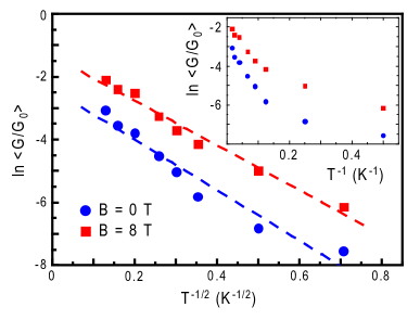
We now look at the temperature dependence of the conductance measured in the transport gap. For strongly localized electrons, transport occurs via either nearest neighbor hopping (NNH) or variable range hopping (VRH) Books , and the latter mechanism dominates at low temperature. Fig. 5 shows the measurement of the gate-averaged conductance in the transport gap as a function of temperature in the range K, for T and T. In case of NNH, the temperature dependence of the conductance should be proportional to . However, the plot shown in the inset of Fig. 5 indicates that Arrhenius law does not reproduce the data well. Rather, the data fits better to , which is the temperature dependence expected for VRH (see Fig. 5). The exponent corresponds to two-dimensional hopping in the presence of Coulomb interaction (which is expected given the obvious presence of Coulomb-blockade effects), or for quasi one-dimensional hopping with or without interactions. This behavior indicates that electronic transport is dominated by variable-range hopping.
The parameter is related to the energy needed by an electron to hop between localized states. From the linear fit to the data of Fig. 5 we obtain meV at T and a smaller value, meV at T when time reversal symmetry is broken. This result agrees with what we would expect if is larger at high magnetic field. Indeed, the relevant energy scales of the localized states involved in the hopping are the single-particle level spacing and the charging energy, which are inversely proportional to the extension of the wave-function of the localized states (i.e., they decrease when increases). The values found for are, as expected for the variable range hopping regime, a fraction of the characteristic values of single level spacing and charging energy, which, depending on the detail of the estimate range from about 10 meV to a few tens of meV (at T, with nm).
In summary, magneto-transport experiments provide a consistent picture as to the origin of the transport gap observed in graphene nano-ribbons: they indicate that strong-localization effects –and not a gap between valence and conductance band– are the cause of the observed insulating state that is observed experimentally.
Acknowledgements.
We thank Y. Blanter, L. Vandersypen, M. Fogler for useful discussions, and S. Russo for support in fabricating several devices. This work was supported by the NWO VICI, NanoNed, the Swiss National Science Foundation (project 200021-121569), and by the NCCR MaNEP.References
- (1) A. K. Geim, K. S. Novoselov, Nat. Mater. 6, 183-191 (2007)
- (2) K. Nakada et al., Phys. Rev. B 54 (24), 17954 (1996); Y. -W. Son, M. L. Cohen, S. G. Louie, Phys. Rev. Lett. 97, 216803 (2006); L. Brey, H. A. Fertig, Phys. Rev. B 73, 235411 (2006)
- (3) M. Y. Han et al., Phys. Rev. Lett. 98, 206805 (2007)
- (4) Z. Chen et al., Physica E 40, 228-232 (2007); K. Todd et al., Nano Lett. 9, 416 (2008); C. Stampfer et al., Phys. Rev. Lett. 102, 056403 (2009); X. Liu et al., Phys. Rev. B 80, 121407 (2009); P. Gallagher, K. Todd, D. Goldhaber-Gordon, arXiv: 0909.3886 (2009)
- (5) F. Sols, F. Guinea, A. H. Castro-Neto, Phys. Rev. Lett. 99, 166803 (2007); D. Gunlycke, D. A. Areshkin, C. T. White, App. Phys. Lett. 90, 142104 (2007); A. Lherbier et al., Phys. Rev. Lett. 100, 036803 (2008); M. Evaldsson et al., Phys. Rev. B 78, 161407 (2008); E. R. Mucciolo, A. H. Castro-Neto, C. H. Lewenkopf, Phys. Rev. B 79, 075407 (2009); I. Martin, Y. M. Blanter, Phys. Rev. B 79, 235132 (2009)
- (6) S. Russo et al., Phys. Rev. B 77, 085413 (2008)
- (7) M. Y. Han, J. C. Brant, P. Kim, Phys. Rev. Lett. 104, 056801 (2010)
- (8) The enhanced disorder in nano-ribbons probably orginates from a combination of intervalley scattering due to atomic-scale edge roughness, and larger potential fluctuations due to chemical species saturating the dangling bonds at the edges.
- (9) B. I. Shklovskii, A. L. Efros, Electronic properties of doped semiconductors (Springer, Heidelberg, Germany, 1984); Y. Imry, Introduction to mesoscopic physics (Oxford Univ. Press, Oxford, UK, 1997); Y. V. Nazarov, Y. M. Blanter, Quantum transport: introduction to nanoscience (Cambridge Univ. Press, Cambridge, UK, 2009)
- (10) M. E. Gershenson et al., Phys. Rev. Lett. 79 (4), 725-728 (1997)
- (11) F. V. Tikhonenko et al., Phys. Rev. Lett. 100, 056802 (2008)
- (12) K. S. Novoselov et al., Nature 438, 197 (2005); Y. Zhang et al., Nature 438, 201 (2005)
- (13) At 8 tesla the energy gap between the lowest Landau levels is much larger than the expected band-gap: since features associated to Landau levels are not visible, the much smaller band-gap should also not be expected to determine the device properties.