Empirical comparison of high gradient achievement for different metals in DC and pulsed mode
Abstract
For the SwissFEL project, an advanced high gradient low emittance gun is under development. Reliable operation with an electric field, preferably above 125 MV/m at a 4 mm gap, in the presence of an UV laser beam, has to be achieved in a diode configuration in order to minimize the emittance dilution due to space charge effects. In the first phase, a DC breakdown test stand was used to test different metals with different preparation methods at voltages up to 100 kV. In addition high gradient stability tests were also carried out over several days in order to prove reliable spark-free operation with a minimum dark current. In the second phase, electrodes with selected materials were installed in the 250 ns FWHM, 500 kV electron gun and tested for high gradient breakdown and for quantum efficiency using an ultra-violet laser.
pacs:
68.37.Vj, 29.25.Bx, 32.80.-t, 32.00.00I Introduction
The Paul Scherrer Institut (PSI) is interested in constructing and operating a 4th generation light source before the end of the next decade. This X-Ray Free Electron Laser (XFEL), operating at = 1 Å, will be a companion to the existing 3rd generation light source, the Swiss Light Source. The SwissFEL (previously PSI-XFEL) facility, in order to fit the site and the budget constraint, needs a concept which reduces the required beam energy given by the desired radiation wavelength according to the spatial coherence criterion, see equation 1
| (1) |
where is the normalized transverse emittance at the undulator entrance, and being the relativistic coefficient Leeman:2007 ; Oppelt:FEL07 .
In order to produce a low emittance beam, studies on a prototype diode electron gun have been performed. The diode should sustain the highest possible gradient in order to accelerate a high charge density beam and minimize emittance dilution due to space charge effects. The goal is to exceed typical values of accelerating gradient achieved in state of the art photoguns ( 100 MV/m). As discussed in lepimpec:2007 , reviewing over a century of research on vacuum breakdown is not sufficient to select the appropriate material for a specific application.
Metallic electrodes, with different preparation procedures were first tested in a 100 kV DC system, and the results obtained compared to the literature. Parts of those results were already presented in lepimpec:2007 . As the diode prototype came on line high gradient (HG) high voltage (HV) tests were carried out with and without the UV laser. The results, including quantum efficiency (QE) measurements, are reported in this paper.
II 100 kV DC System
The ultra-high vacuum (UHV) chamber shown in Fig.1, is described in detail in lepimpec:2007 . The UHV system comprises a diode ion pump of 150 l/s, an injection line, a leak valve and a capacitance pressure gauge. The gauge measures the absolute pressure of the injected gas (Ar, He or a mixture of both) in order to prepare for plasma glow discharge (PGD) between the electrodes ( 20 minutes, 500 eV, pressure.distance 1 torr.cm). Polished electrodes were treated using only Argon gas, providing ions of 400 eV (ArPGD). The ion current was 10 mA spread over a few cm2 of electrode. PGD for the rough electrodes were, at first, a mixture of He-Ar followed by pure Ar lepimpec:2007 .
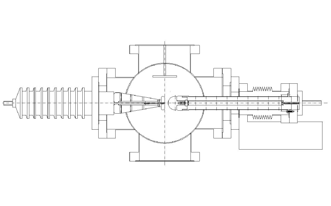
A negative DC bias of 0 to 100 kV is applied to the cathode through an insulating ceramic, (on the left in Fig.1). The anode is grounded. In principle the power supply can deliver up to one mA at 100 kV. It is possible to adjust the maximum current allowed to be delivered by the power supply; we have adjusted it around one microA. The potential energy stored in the system is 1.5 J at 100 kV. The current flowing from the cathode to the anode is measured across a 1 M resistor with a Keithley multimeter and recorded with Labview™ software. The gap separation between the electrodes is adjustable with a translation feedthrough and is measured with a digital micrometer. A photomultiplier (PMT) is used to detect X-ray (XR) activity.
Usually one pair of electrodes is tested. They are then re-machined and polished for subsequent tests. In the cases of copper, aluminium and stainless steel two different pairs have been used.
II.1 Non Polished Electrodes
The modus operandi and a first set of results were published in lepimpec:2007 and is summarized in Table 1. The electrodes were, for the most part, rough machined and their average surface roughness (Ra) is below, but close to, 200 nm. The highest gradients were usually obtained after the first in-situ PGD cleaning but sometimes after a second. The values quoted for 1 nA were, in general, obtained after arcing. After arcing, field emission (FE), or ”dark current”, appears for lower gradients. A subsequent PGD can often restore the gradient without FE.
| Cthd-And | Dark Current | As Received | After PGD |
| SS-SS | nA | 40 | 68 |
| 1 nA | 42.5 | 35 | |
| Ti-Ti | nA | 50 | 63 |
| 1 nA | 46.6 | 67 (0.1nA) | |
| Ti-Ti | nA | 29.6 | 39 |
| Vac Fired | 1 nA | 32.5 | 41.4 |
| Mo-Mo | nA | 37 | 44 |
| Vac Fired | 1 nA | 45.2 | 61.3 |
| Cu-Cu | nA | - | 32 |
| Oxidized | 1 nA | - | 29.3 |
| Cu-Cu | nA | 24 | 55 |
| Etched | 1 nA | 26 | 19 |
| Cu-Mo | nA | 18.2 (3mm) | 21.6 |
| 1 nA | 13.8 (3mm) | 25.4 | |
| Al-Al | nA | - | 52 |
| 1 nA | 7.5 | 30 | |
| Al-Al | nA | 36 (2mm) | 73 |
| (*) | 1 nA | 29 | 31 |
| Nb-Nb | nA | - | 10 (4mm) |
| 1 nA | - | 5.5 (4mm) |
| SS: Stainless steel ; (*) Mirror-finished - damaged anode |
The PGD between the electrodes is obtained by biasing the upper, third, electrode positively up to 500 V and connecting the anode-cathode pair to ground lepimpec:2007 . This configuration cleans the electrode pair in a similar manner. Applying the bias to each electrode, one after the other, frequently results in transferring contaminants from one electrode to the other. However, in DC mode a breakdown is generally cathode initiated springer5 . Therefore, cleaning the cathode last can still be beneficial in reaching high gradient.
Most of the metals tested in this first sample set reached their breakdown gradient without arcing. Ti and Mo sustained a few micro-breakdowns before arcing. Micro-breakdown in this system is characterized by a surge in pressure, followed by a burst (a few seconds) of FE current. A definitive breakdown is defined and characterized by a sustained vacuum activity. The pressure is often ten times higher than during normal operation, and the FE current is such that the 100 kV power supply cannot hold the voltage. Electric gradient values are then recorded when the FE current is set to 1 nA, to compare with the literature Furuta:Nima2005 . This explains why values at 1 nA are generally lower than the values without FE (0.05 nA), as in the case of the etched Cu after PGD, Table.1
II.2 Polished Electrodes
Electrodes were polished or diamond turned by commercial companies capable of producing high quality optical mirrors. The average roughness, Ra, of the polished electrodes was below 40 nm, and below 10 nm for Al, Cu and SS. The term ”mirror-finished” will refer to surfaces with average roughness below 40 nm. The breakdown gradients obtained were compared to those obtained for polished electrodes of broad area. Furuta:Nima2005 ; diamond1:98 ; Wang:2003 . Nb, Ti and Mo electrodes were, prior to polishing, given high temperature (HT) treatment and the Nb electrodes were treated with buffered chemical polishing (BCP). HT treatment refers to vacuum firing in a dedicated furnace at CERN (Conseil Européen pour la Recherche Nucléaire) following CERN procedures for each material. One of the criteria in the choice of temperature is to avoid excessive re-crystallization Calatroni . The temperature plateau of the furnace is set at 900∘C for 2h for SS; Ti, Mo and Nb at 800∘C for 6h. Getter material such as Ti are placed inside a separately pumped and degassed vacuum container to avoid any contamination of the electrode by outgassing gas from the furnace. In the case of Nb, after BCP, grains up to 10 mm size were visible. HT treatment, with a sufficiently high temperature, reduces the number of field emitters Niedermann:1986 . In this case the temperature chosen for Nb is below this critical temperature, hence the need for polishing. All electrodes are measured as-received after a careful ethanol wipe before mounting in the UHV chamber. The first PGD is made after the installed as-received cathode either arcs or emits a dark current of 1 nA.
Table 2 summarizes the best results. PGD almost invariably improved breakdown gradient. Electrodes installed ”as-received” were only cleaned with alcohol (ethanol) before being installed in the vacuum chamber. The values quoted for 1 nA, were usually obtained after arcing, hence the lower numbers compare to the 0.05 nA row. In the ”as-received” case the values of the field recorded in the 1 nA row are higher, as FE appears before breakdown. After test, all electrodes retained their mirror like appearance, except for the damaged area, however no roughness was measured.
| Cthd-And | Dark Current | As Received | After PGD |
| Cu-Cu | nA | 20 | 67.5 (*) |
| 1 nA | 25 | 67.5 (*) | |
| Cu-Cu | nA | 37 | 52 |
| New-Used | 1 nA | 41.9 | 47 |
| SS-SS | nA | 65 | 71 |
| 1 nA | 24 | 25 (0.1nA) | |
| Nb-Nb | nA | 20 | 59 |
| 1 nA | 23 | 20.8 | |
| Mo-Mo | nA | 32.5 (2mm) | 68.5 |
| 1 nA | 32 | 33 |
| (*) Drift from 0.03nA to 8.5nA in 58 hrs |
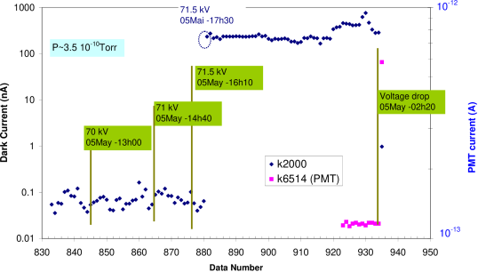
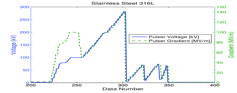
Operation at a given gradient was carried out over periods of days. As an example Fig.2 shows the results for SS mirror-finished electrodes at 1 mm gap after PGD. Each data point is an average of 10 measurements and was recorded at intervals of 10 minutes. The system was stable at 69 kV for 6 days. A sudden increase of dark current was probably due to a micro breakdown. The drop in voltage at the end of the sample is due to a software protection scheme, which switches off the high voltage (HV) power supply when voltage drops by more than 1 kV from the set value. The drop in voltage is usually due to a higher emission of dark current. The PMT signal often correlates with FE activity, and is enhanced with increasing vacuum level. In this setup the PMT is placed behind a window, facing the electrodes gap. With a 4 mm gap, a clear PMT signal can be recorded, but as the gap closes, the amount of XR going through the PMT drops significantly.
In general, and after PGD, results obtained for the non polished electrodes (Table.1) and polished electrodes (Table.2) in a DC regime are not so different.
For Nb, polishing followed by a PGD (Table.2) permitted much higher fields to be achieved compared to non polished electrodes (Table.1). Polished Mo did not exceed 40 MV/m, without FE, even after two consecutive Ar PGD. In order to reach 68.5 MV/m, the Mo cathode was run with a 6 A, 50 kV, dark current for 72 hours. A third Ar PGD of 2 hours followed; the best result is shown in Table.2. The main action of the PGD is to remove contaminants on the surface hence changing the work function of the surface of the material with little change of the surface topology Cernusca ; springer5
When compared to ref.Furuta:Nima2005 an in-situ PGD gives results equivalent to those after careful polishing followed by an ultra-pure high pressure water rinsing. In general a PGD treatment used on a commercially mirror-finished or non mirror-finished electrode gives significant improvement compare to an ”as Received” electrode. A literature comparison, Table 3, to our results proves that the breakdown field (BF) quality from mirror-finished surfaces, either by polishing or diamond turning, coming from commercial vendors is, nowadays, very satisfying. Microscopy analysis does not show systematic embedded material, roughness achievement is equivalent, and sometimes superior to, that which a research laboratory can produce. One surprising point is the fact that in general PGD on rough material gives some very competitive results compare to highly polished, hence expensive, material.
| SS | Cu | Ti | Mo | Mo - Ti | Al | Nb | |
| Furuta - 1 nA Furuta:Nima2005 | 36 | 47.5 | 88 | 84 | 103 | - | - |
| Diamond - No FE diamond1:98 | - | 70 | 60 | - | - | 85 | 92 |
| Kranjec - BF Kranjec:67 | 79.8 (*) | 46.1 | 48 | 38.9 | - | 51.3 | - |
| CERN - saturated BF Descoeudres:EPAC08 | 800 | 170 | 780 | 420 | - | 150 | 400 |
| Tarasova - saturated BF springer5 | - | 46 | 55 | 62 | - | 45 | 48 |
| Best BF (this work) | 71 | 67.5 (**) | 67 | 68.5 | - | 92 (***) | 59 |
| (*) Measured at 0.5 mm | (**) 8 nA of dark current | (***) measured at 0.75 mm |
In early works, it was stated that the less refractory metals seem to reach the highest breakdown field Brodie:66 ; Kranjec:67 . From results presented in Table 3, this is not so evident. Moreover, results from CERN contradict this conclusion with Ti, V, Cr, Mo, Nb, Ta and W holding higher gradient than soft materials like Cu and Al, as also shown in much older work springer5 . CERN and results cited in springer5 are obtained by doing breakdown conditioning; at CERN between a pointed anode and a flat cathode with gaps around 20 m Descoeudres:EPAC08 , and for ref.springer5 between different kind of electrodes separated by gaps varying from 0.3 mm to 5 mm, hence a very different modus operandi. In order to compare data presented in line 3 of Table 3 to other results, the electric field in MV/m has been derived by calculating back from the original voltage.
Different preparation will results in a different enhancement factor () and a lower results in general in a higher BF, although not always Suzuki:Nima2001 ; Furuta:Nima2005 . Using is a convenient way to compare FE quality because it is usually a straight line fit of the data when plotted in a Fowler-Nordheim plot (ln(I/V2) vs 1/V) and should not present any discontinuity Kranjec:67 ; springer5 . It is particularly well suited in comparing electrodes of the same materials prepared in an identical way, prior any high gradient testing. However, the intrinsic understanding of on a ”dirty” surface, in a UHV sense, is absent. For example, a variation of the chemistry on the surface implies a variation of the work function. However, as the work function is systematically never measured, but assumed, this variation will be attributed to a change of in the Fowler-Nordheim equation. Our point is that comparing directly the emission current versus the field applied gives an immediate conclusion. In most of our results the FE current, before breakdown, is below the detection limit, as in Fig.2. Hence comparison is not feasible.
The electrodes tested were single material. A mix of different electrode materials is certainly promising for reaching high gradient in real DC gun Furuta:Nima2005 , as one of the hypothesis of the breakdown is material transfer from the anode to the cathode springer5 . Unfortunately our pulse has an oscillatory behavior with a positive peak amplitude being 60% of the negative peak, Fig.5. As the effect of the anode cannot be neglected, we have concentrated our effort on single materials in order to propose usable solutions for our needs, without complicating our research.
III 500 kV Pulsed Diode prototype electron source
It is known that higher gradients are achieved when using a pulse high voltage compared to a DC system springer5 ; Smedley:2003 . This is also true in an RF system where the short pulse permits a higher gradient to be reached Doebert:PAC07 .
The original SwissFEL concept was based on a field emitter array (FEA) producing an electron beam of 5.5 A in 2 ns (FWHM) Bakker:2004 . In order to produce an electron beam with no or little energy spread either a jitter free square pulse or a longer pulse is needed. The 500 kV - 250 ns (FWHM) pulser, Fig.3, was initially designed to accommodate such a requirement.
The main driving factor for having HV transformer technology is the compromise between stability and complexity. In the voltage range considered (0.5 - 1 MV), the only available hard switch is a gas switch (spark gap). Self-triggered gas switches are not suitable for large dynamic range because switching parameters depend strongly on operating voltage. Another disadvantage is large switching time jitter and limited life. Triggered gas switches are much more suitable in terms of jitter but require a fast HV trigger pulse or a high power short laser pulse. Switching characteristics of electrically triggered gas switches still depend on applied voltage and to ensure good dynamic range and jitter performance, they require fast trigger voltage pulses with amplitude comparable to the switched voltage Williams:89 . This requirement makes such a system impractical. Performance of laser triggered gas switches depends on the properties of the laser trigger pulse. Using lower laser peak power (several MW) the jitter performance is still in tens of nanoseconds (peak) Hutsel:08 ; Vyuga:PPC03 . Recently, research groups have reported good results with high peak power laser triggered gas switches Luther:2001 ; Hendriks . In order to get dense enough photo-excited plasma in the conducting channel, the trigger laser has to provide pulses with tens of GW to TW peak power. That dramatically increases the complexity and the cost of such a system. Thyratron switched air-core resonant transformer, combined with relatively high primary voltage, gives a good speed - stability engineering compromise and makes it possible to achieve the required amplitude stability to better than 0.1% Paraliev:IPMC08 . The linear system ensures large dynamic range of the output voltage, required for such test system. Another reason to use a fully linear technology is the scalability.
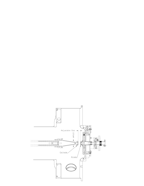
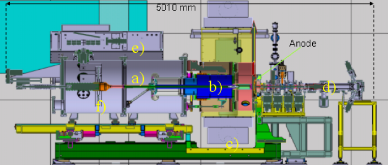
A more detailed cross section of the UHV vacuum chamber with the electrodes for the high gradient pulsed tests is shown in Fig.4. The laser illuminating the cathode is inserted in the middle of the beam line after the UHV valve Fig.3 and goes through the 2 mm diameter anode hole. The chamber is sealed without bolts, using a differential vacuum system. This permits easy exchange of electrodes. The chamber is integrated into a filtered air cabinet (shown in green in Fig.3) to ensure a dust-free environment when it is opened. With a turbo pump, a pressure of 10-7 mbar can be reached in 12 hours, and with two 300 l/s ion pumps, 10-8 mbar can be reached within two days. The cathode support includes provision for future mounting of FEAs which are presently under development at PSI Soichiro:IVNC07 . The pulser uses thyratrons and an air-core transformer (Tesla coil) to generate a damped oscillating waveform with a dominant negative peak voltage Paraliev:USA05 ; Paraliev:IPMC08 . The peak voltage, when above 30 kV, is stable to 0.1% and can be varied from 0 kV to 500 kV. The gap between the electrodes is adjustable from 0 to 30 mm. Both electrodes are made of the same material and have the same profile, unlike the previous 100 kV DC system. For quantum efficiency (QE) or electron beam emittance measurements, the emitted electron beam passes through a 2 mm diameter anode hole. The diagnostic beam line, shown in Fig.3, includes five solenoids to transport and focus the beam. After the first solenoid, which is mounted on the pulser flange, a wall current monitor is installed. A Faraday cup or a YAG screen can be inserted in the beam line. They are located 491 mm downstream of the anode. An emittance monitor of 870 mm long fitted with movable pepper pot and YAG screen is used for emittance measurement. It is located at the end of the beam line. The overall length of the diagnostic line from the pulser flange to the end of the emittance monitor is 1470 mm. A more detailed description of the 5 m long beam line, including the 3.4 m long pulser, can be found in Pedrozzi:EPAC08 .
Fig.5 shows a typical pulser trace with a 4 mm gap. The upper trace labeled C2 is a collection of waveforms of the quasi DC pulse. The pulse oscillates up to 10 s; 8 s are displayed in Fig.5. This oscillation, and the superposition of a 950 kHz and a 1800 kHz signal, results from the choice of technology Paraliev:USA05 . The amplitude of the second positive peak is 60% of the maximum of the first negative peak.
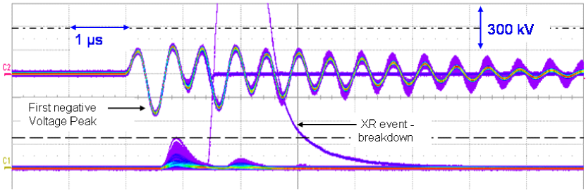
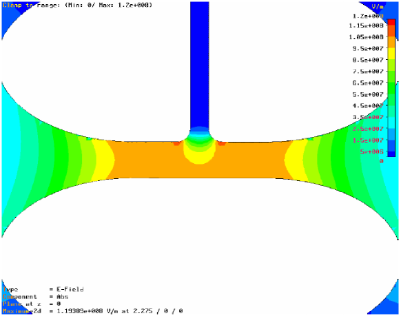
The oscillatory voltage waveform of the pulser, with still a high amplitude of the positive peak, was the reason to concentrate our effort on electrode pairs of the same material in the 100 kV DC test stand. Fig.6 shows the electric field at different locations of the pulser electrodes’ surfaces.
An XR scintillator detector is used to detect breakdown. The XR scintillator signals, multiple traces, labeled C1 are delayed with respect to the negative voltage peaks because of an analog filter delay. When a spark occurs, the XR signal saturates as is seen for one event in Fig.5; this high level is used as a machine protection system and will stop the HV pulsing until reset, or at least until the HV is reduced. Breakdown is characterized by watching the camera pointing toward the electrodes, the cathode voltage and XR signals. Considering Fig.5 in more detail, the spark occurred at a moment when the HV was low, suggesting that the previous positive voltage swing may have contributed. The HV is clamped to a flat line with almost zero voltage indicating that all energy is dissipated in the spark turning it into a destructive arc. The video camera image shows a bright uniform arc column between anode and cathode and the scintillator signal saturates for a few s. In general, more than 2/3 of the events happen at the first negative voltage peak. The scintillator will saturate, but the pulser will not systematically display a flat line.
A total of 24 electrode pairs were tested, with evolving skill for polishing and cleaning. The reason for developing in-house polishing technics, instead of buying pairs from vendors, is from the possibility of high turn over in electrode exchange. The range of breakdown gradients achieved, for gaps varying from 2 mm to 6 mm, is shown in Table 4. Highest gradient were obtained for the smallest gap. For reasons of cost and ease, most measurements were obtained with 316L stainless steel and OFE copper, with typical average roughness below 15 nm. Although many factors might affect breakdown, the dominant factor for this gradient level is the quality of mechanical polishing, mainly characterized by roughness and some microscopy to pinpoint embedded polishing material. The hand polished procedure starts with the use of abrasive paper from coarse to fine grains. For SS, diamond paste of decreasing diamond particles size is then used. For Cu, polishing paste LUXORTM 0.1Mu is used, instead of diamond paste; wipe of the paste is performed using ethanol.
Before closing the vacuum chamber all electrodes are spray cleaned with dry ice, for a few seconds. First results on Nb were obtained with an electrode prepared at CERN, using the BCP technique, which again exposed the big grains of the material. Higher results (83 MV/m) were obtained after hand polishing, which did not expose the underlying grain structure of the electrode so completely hence reducing the roughness. SS and TiVAl achieved the highest gradient although they are alloys. It seems that material purity is not an important parameter. So far, we have not seen any influence of the electrode geometry, e.g. the anode hole, on breakdown rate or breakdown location.
| Cthd-And | without laser | Duettino® laser | Jaguar® laser |
| CuCr - CuCr | 23 | - | - |
| WCr - WCr | 30 | - | - |
| Al - Al | 46 | - | 50 |
| Cu - Cu | 74 - 83 | 41 - 51 | 50 - 63 |
| Nb - Nb | 60 - 83 | 64 | - |
| SS - SS | 70 - 140 | 95 | 50 - 80 |
| TiVAl - TiVAl | 70 - 130 | - | - |
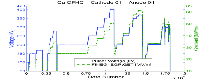
Typical operation for HG achievement, without laser, is shown in Fig.7 (left figure). The voltage (solid line) for a given gap is raised in steps of a few kV after a given number of pulses. The voltage increases until a breakdown occurs. At this moment the voltage is decreased and ramping up is resumed. This procedure is used with and without laser operation. In this example, the hand polished SS electrodes did not survive the first breakdown, as gradient could not be restored by subsequent breakdowns. Operation lasted for 31 minutes. The right figure of Fig.7 displays a typical laser operation. First at large gap then at smaller gaps. This procedure is the standard procedure used for all electrodes illuminated with a laser. The corollary of this procedure is that an electrode holding high voltage at small gap will hold the same voltage at large gap. We routinely observe this behaviour each time we resume operation, day to day, with the installed electrode pair. The constant voltage plateaus signify gap change or QE measurement. In this example, the diamond turned electrodes broke down at 61 MV/m and the gradient could not exceed 50 MV/m. Operation lasted for 10 hours. The longest operation at high gradient, without breakdown, was obtained with SS electrodes : 80 MV/m for 9 hours and extracting 55 pC of electron beam current. Routine operation for emittance measurement at 50 MV/m (6 mm gap) over days, is achieved with either Cu or SS electrodes. The simple hand polishing technique used can allow a damaged electrodes to be refurbished in half a day and be able to be processed (in general discharge free) to 50 MV/m.
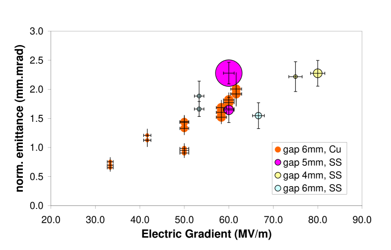
The charge produced by the laser lies between 1 pC to 80 pC depending of the needs. The goal of this electron gun, in its original concept, is to produce a low emittance beam at high voltage and gradient. During cathode testing, no systematic emittance studies were done, but still some normalized transverse emittance (geometric average ) as function of the beam energy were measured, Fig.8 Oppelt . The beam charge, represented by the circle size, ranges from 10 pC to 154 pC and most emittances measured lie between 0.5 mm.mrad and 2 mm.mrad. Emittance measured with Cu cathodes shows that in general smaller emittance were obtained for small charges. We could not correlate small emittance for high gradient at similar charges, orange circles in Fig.8. Results on SS were even more inconclusive.
In the 100 kV DC system PGD have shown to be pushing back the onset of the breakdown threshold, even on mirror surfaces. In the pulser we used an external DC power supply to bias the cathode positive or negative in order to light up ArPGD. The plasma could be localized between the electrodes only for a given set of voltage (200 V), current and gas pressure (usually a few Torr), and this was largely independent of the gap between the electrodes. With such parameters and configuration, the energy of the ions was probably much less than 200 eV. Later attempts used the pulser itself, running at 50 Hz to give a kilovolt pulse across the gap. Unfortunately, the large gap current meant that the cathode had only a positive half-cycle of some microseconds. PGD treated electrodes did not perform better than untreated electrodes.
As expected, the gradients and voltages achieved for the pulsed diode system (Table.4) with gaps varying from 2 mm to 6 mm are above the one obtained in DC system with large gap (1 mm to 4 mm) (Table.3). Moreover DC breakdown test using pulser’s electrodes design, Fig.6, with SS and Cu electrodes, prepared similarly as the one installed in the pulser, holding the dry ice spray, have reach gradient similar to gradient quoted in Table.3, respectively 69 MV/m and 63 MV/m at 1 mm gap.
IV Quantum Efficiency of Metals
A collection of quantum efficiency, or photoelectric yield curves for ”dirty surfaces”, in the UHV sense, and for photon energy above 10 eV, is summarized in Redhead:68 . QE for clean and ”dirty” copper for wavelength above 20 nm can be found in Phelps:1999 .
Two laser systems, from Time-Bandwidth Timebandwidth , were used to measure the QE of the metals. The first laser system used to measure the QE of the material is described in Pedrozzi:EPAC08 . The main parameters of the Duettino® laser beam are : = 6.5 ps rms, = 266 nm (4.66 eV), energy 12 J/pulse at laser exit; energy at the entrance of the accelerator beamline 4 J ( 5% peak to peak). The main parameters of the second laser system, Jaguar®, are : = 13 ps rms (or 35 ps FWHM), = 262 nm (4.73 eV), energy 400 J/pulse at laser exit; energy at the entrance of the accelerator beamline 200 J ( 0.5% peak to peak) without any laser beam shaping pinhole. The short term laser pointing stability, for both lasers, at a virtual cathode position was measured to be around 10 m rms. The size of the laser beam on the cathode is chosen such that its power density stays below 150 MW/cm2, typically the beam size is in the order of a mm when using the Jaguar® and was halved when using the Duettino®.
As represented in Fig.10, the quantum efficiency (QE) increases with the applied electric field due to the Schottky effect.
6.5cm
![[Uncaptioned image]](/html/1003.3594/assets/x10.png) Figure 9: QE increase for a Cu cathode after 1 month of laser and high voltage operation.
Figure 9: QE increase for a Cu cathode after 1 month of laser and high voltage operation.
![[Uncaptioned image]](/html/1003.3594/assets/x11.png) Figure 10: QE of copper, stainless steel and niobium
Figure 10: QE of copper, stainless steel and niobium
Indeed analytical formulae Dowell:2006 based on the three steps model (absorption, excitation and emission of electrons) Dubridge reproduce quite well the measured data points. The only parameter in equation 2 that has been adjusted is the work function, which depends mainly on the surface material and crystal orientation. The reflectivity R, of a given metal, is measured in air.
| (2) |
Where EF is the Fermi energy, Eph = is the photon energy, is the laser penetration depth, is the electron - electron scattering length and Em is the energy above the Fermi level. is the effective work function, which is the work function of the bare material minus the barrier reduction due to the external field applied, see equation 3
| (3) |
The plot of equation 2 in Fig.10 shows a good match with the experimental values. The parameters used for copper Dowell:2006 are : RCu(266 nm) = 0.25; EF = 7 eV; Eph = 4.6 eV; = 10.7 nm; = 2.2 nm.
The difference between the two Cu measurements can be interpreted as a cleaning (contaminants removal) of the surface after one month of operation; no breakdown occurred during that period. The maximum QE measured was on the order of 2.10-5 at 25 MV/m, which is in agreement with copper based RF photogun measurements Akre:2008 . Fig.10 shows the QE of various metals measured with this beamline Pedrozzi:EPAC08 .
Laser cleaning can also be efficient if the power density stays below the ablation threshold, in order to preserve emission uniformity at the surface. Some experimental results can be found in Akre:2008 ; kirby:QE06 . As in the DC system, where ion cleaning (PGD) has improved the field holding, ion cleaning can also improve the QE Dowell:2006 . The effect being mostly to reduce the work function, by removal of the oxide of the surface, to equal the work function of the pure material, without drastically changing the surface morphology. Arcing changes the chemistry and topology of the surface; its effect on the QE is seen as soon as the pulser system recovers from the arc. The tendency is that the QE is increased after an arc. Breakdown conditioning will definitively clean the surface and is an efficient process for RF accelerator structure conditioning, but is allegedly detrimental for an electrode which should produce a uniform beam.
The following figures illustrate the effect of breakdown on the QE of Cu, Fig.11, and SS, Fig.12. The data were obtained using the Jaguar® laser.
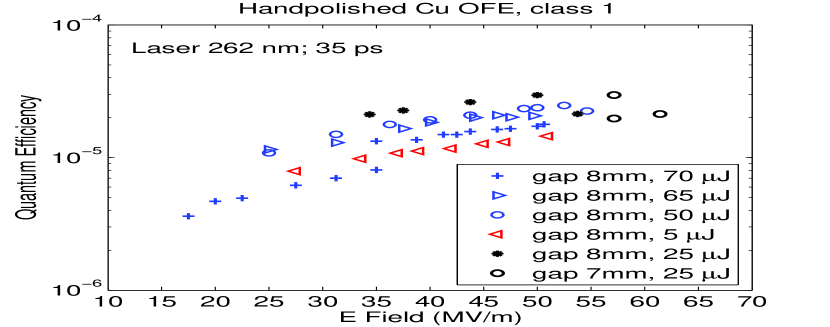
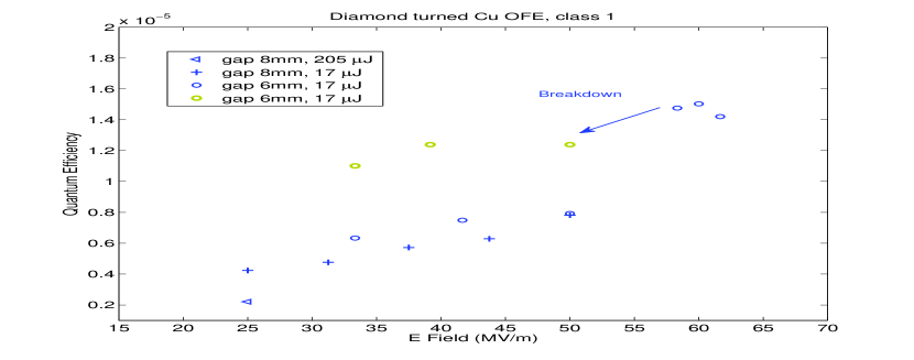
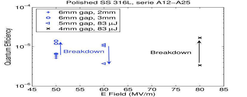
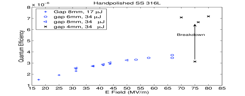
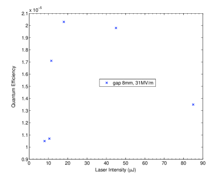
The QE displayed in the left figure of Fig.11, were obtained using a pre high gradient (83 MV/m) conditioned pair of Cu electrodes. On the right figure, pristine diamond turned Cu electrodes were installed. 200 pC could be extracted using 50 J of laser intensity. Our electron beam with charges of 10 pC and above is space charge dominated. The collection of all charges on the Faraday cup might not be linear with the laser intensity for gradients below 40 MV/m. Depending of the laser intensity falling on the cathode the electron emission can be hampered by the field produced by the already emitted electron, even using ps long laser pulse. In Fig.11 (right plot), the QE of a pristine Cu cathode, at 25 MV/m electric field, is twice less when using 205 J of laser energy than when using 17 J. We tested the QE of the same diamond turned Cu cathode versus the laser energy, Fig.13, at 31 MV/m after the electrode pair had sustained few breakdowns. Again for laser intensity in excess of 40 J, the process of electron production became inefficient. For gradient in excess of 60 MV/m linearity with the laser intensity up to 80 J is ensured. For laser intensity up to 34 J, QE linearity is insured from field above 35 MV/m, as can be seen in Fig.12, right plot, as the QE is identical for two laser intensities 17 J and 34 J. The QE of pristine SS electrode is slightly inferior, for a given gradient, to the QE of a pristine Cu; see Fig.12 right figure compared to Fig.11 right figure. As for Cu, breakdown generally increases the QE and spoils the emittance of the electron beam. However, as for Cu, a few breakdowns ( 5) are usually necessary to significantly degrade the beam emittance.
Finally the 262 nm UV light reflectivity of some electrodes were measured, in air, after breakdown test. The light was collected at an angle of 30 degrees. The reflected light in the damaged area (craters) was still very specular except for Nb where strong stray light could be observed. One should then be careful in estimating the QE of a damaged photocathode with equation.2 as we did not collect the light over all angles.
| Copper | 316L SS | Molybdenum | Niobium | |
|---|---|---|---|---|
| Pristine area | 25.4% | 17% | 40.5% | 12% |
| Damaged Area | 6.4% | 7.3% | - | 10.5% |
V Conclusion
In the quest to find a good material, capable of holding high gradient ( 100 MV/m) and producing a 200 pC electron beam; we have tested electrodes of different material and with different preparation procedures. We mainly compared polished and diamond turned (for non ferrous material) electrodes to non polished one with and without plasma glow discharge. Those results were also tested versus results found in the literature. The main criteria being that the material should reach the target gradient and voltage without arcing. Any arcing being detrimental to the emittance of the beam to be produced or could transfer foreign material onto the electron source, effectively deteriorating this one. This is especially true for metals of low melting point like Aluminium.
The important results of the first section is that polishing (40 nm average roughness) does not give one much advantage in the attainment of high gradient compared to rough electrodes (200 nm average roughness) which have been cleaned in-situ by an Ar PGD. However, in the absence of PGD, polishing and good cleaning before mounting is mandatory. Nowadays industrial companies do produce electrodes of equivalent surface finish (geometrically and chemically) than in-house production, with suitable and reproducible results for our high gradient needs. The choice to either develop in-house a polishing recipe or buy polished electrodes from external vendor, depends on the turn over time and price to obtain new electrodes and not on the quality of gradient achieved as they both gave similar end results. The PSI in-house recipe, which mainly depended on human skill, took two month to master and allowed us to refurbished an electrode pair in half a day.
The overall high gradient results obtained can be directly of use for DC guns like the 500 kV DC gun used at Jefferson Laboratory, a gun design which is now widespread in the FEL/ERL community Sinclair:2006 . In this remark we are of course not suggesting that a steel cathode holding 69 MV/m at 1 mm under DC voltage will hold the same gradient at 10 mm. We are instead suggesting material and possible preparation methods to be used for those guns. One has still to remember that using the ”same” preparation technics does not, unfortunately, necessarily implies the same end results. However, this guarantees still good performances, on routine operation.
In the second part of this work, higher gradients have been obtained using a voltage pulse of 250 ns (FWHM). We have reached the highest gradient with a Ti alloy and SS. Sustained operation with hand polished SS electrodes at 80 MV/m with 55 pC of electron beam extracted was proven for 9 hours. It is not understood why the electrode eventually arced, as it is often the case in this field. Operation, using electron beam with various charges, at 300 kV, 50 MV/m for days without breakdown and no measurable dark current is now routinely achieved, with either SS or Cu, polished, electrodes. In most cases, those electrodes did not arc during the voltage increase. Dark current do exist, as shown by the XR scintillator activity, but the beam is not captured and transported along the beam line.
Cu and SS were found to have QE in the 10-6 range when pristine and for field below 80 MV/m. Breakdown usually rises the QE a decade higher, sometime 2 decades, but degrades the quality of the electron beam. The QE stays constant using different laser energy hence the emitted current scales linearly with the laser energy. This will be true as long as the electric field applied balances the space charge of the extracted beam.
UV (262 nm or 266 nm) reflectivity of the electrodes drops on damaged areas compared to pristine ones. Rough areas trap more light, which makes the surface look black under visible light, hence increasing the QE. Finally, laser ablation threshold from metals depends strongly on the pulse length. For UV laser pulse of 30 ns, the fluence threshold is J/cm2 Ashfold:2003 ; Lorusso:2008 . For picosecond laser pulse the threshold starts around a few 100 mJ/cm2 Preuss:1995 ; Schafer:2002 . Our first attempts to focus the Jaguar® laser beam on a polished Mo cathode, in vacuum and in presence of high voltage, using a beam radius of 300 m and 75 J of incoming UV light, resulted in a hole 100 m deep in the metal. Gradient did not exceed 18 MV/m (100 kV). It seems that to keep the electrode safe from ablation and keep the system arcing free the fluence, as a rule of thumb, should be below 20 mJ/cm2 for picoseconds pulses and in presence of voltage in excess of few hundred kilovolts.
Acknowledgements.
We wish to thanks E. Kirk and T. Garvey for careful proofreading this manuscript.References
- (1) S.C. Leeman, A. Streun, A.F. Wrulich. Phys. Rev. Special Topics - Accelerators and Beams, 10(071302), 2007.
- (2) A. Oppelt et al. Towards a Low Emittance X-ray FEL at PSI. In FEL07, Novosibirsk, Russia, 2007.
- (3) F. Le Pimpec, R. Ganter, R. Betemps. Nuclear Instruments and Methods in Physics Research A, 574:7–16, 2007.
- (4) G.A. Mesyats, D.I. Proskurovsky. Pulsed Electrical Discharge in Vacuum. Springer-Verlag, 1989.
- (5) F. Furuta et al. Nuclear Instruments and Methods in Physics Research A, 538:33–44, 2005.
- (6) W.T Diamond. Journal of Vacuum Science and Technology, A16(2), 1998.
- (7) T. Wang, C.E. Reece, R. Sundelin. Journal of Vacuum Science and Technology, B21(4), 2003.
- (8) S. Calatroni, CERN, private communication.
- (9) Ph. Niedermann et al. Journal of Applied Physics, 59(3), 1986.
- (10) S. Cernusca. Electron Emission and Nanodefects due to Slow Ion Impact on Solid Surfaces. PhD thesis, Technischen Universität Wien, 2003.
- (11) P. Kranjec and L. Ruby. Journal of Vacuum Science and Technology, 4(2), 1967.
- (12) A. Descoeudres, S. Calatroni, M. Taborelli. DC Breakdown experiments for CLIC. In EPAC08, Genoa, Italy, 2008.
- (13) I. Brodie. Journal of Vacuum Science and Technology, 3:222, 1966.
- (14) C. Suzuki et al. Nuclear Instruments and Methods in Physics Research A, 462:337–348, 2001.
- (15) J. Smedley et al. Performance Data of a Pulsed Power Photo-Injector. In 17th Int’l conf Application of Accelerators and Industry, 2003.
- (16) J. Rodriguez et al. 30 GHz High Gradient Accelerating Structure Test Results. In PAC 2007, Albuquerque, USA, 2007.
- (17) R.J. Bakker et al. X-FEL concept based on a low emittance gun, 2004. http://fel.web.psi.ch/public/publications/2004/Bakker-yr04-1.pdf.
- (18) P. F. Williams, F. E. Peterkin. Journal of Applied Physics, 66:4163–4175, 1989.
- (19) B.T. Hutsel, et al. IEEE T. Plasma Sci, 36(5):2541, 2008.
- (20) D. A. Vyuga et al. A 2.5 MV subnanosecond pulser with laser triggered gap for the generation of high brightness electron bunches. In 14th Pulsed Power Conference, 2003.
- (21) B. M. Luther et al. Applied Physics Letters, 79:3248, 2001.
- (22) J. Hendriks. The physics of photoconductive spark gap switching: Pushing the frontiers. PhD thesis, Technical university of Eindhoven, 2006.
- (23) M. Paraliev, C. Gough, S. Ivkovic. Status of 500kV Low Emittance Electron Gun Test Facility for a compact X-ray Free Electron Laser at PSI. In IPMC08, Las Vegas, USA, 2008.
- (24) S. Tsujino et al. Characterization of metallic field emitter array devices fabricated by molding for x-ray free electron laser applications. In IVNC 2007, Chicago, USA, 2007.
- (25) M. Paraliev, C. Gough, S. Ivkovic. Tesla coil design for electron gun application . In 15th IEEE International Pulsed Power Conference, Monterey, USA, 2005.
- (26) M.Pedrozzi et al. First Measurement Results of the PSI 500kV Low Emittancxe Electron Source. In EPAC08, Genoa, Italy, 2008.
- (27) A. Oppelt, PSI, private communication.
- (28) P.A. Redhead, J.P. Hobson, E.V. Kornelsen. The Physical Basis of Ultrahigh Vacuum. Chapman and Hall Ltd, 1968.
- (29) A.V. Phelps and Z.Lj. Petrović. Plasma Sources Sci. Technol., 8, 1999.
- (30) Time-Bandwidth products. http://www.tbwp.com/.
- (31) D. H. Dowell et al. Phys. Rev. ST : Accel & Beams, 9(063502), 2006.
- (32) L. A. Dubridge. Phys. Rev., 43, 1933.
- (33) R. Akre et al. Phys. Rev. ST : Accel & Beams, 11(030703), 2008.
- (34) R. Kirby, D. Dowell and D. Palmer. LCLS Cu Cathodes - Cleaning and Qualification. In High Quantum Efficiency Photocathodes for RF Guns, 2006. http://wwwlasa.mi.infn.it/WSPhotocathodes/dbconnection/DB_All_Presentation_Report.
- (35) C.K. Sinclair. Nuclear Instruments and Methods in Physics Research A, 557, 2006.
- (36) M.N.R. Ashfold et al. Chem. Soc. Rev., 33, 2003.
- (37) A. Lorusso et al. Radiation Effects & Defects in Solid, 163, 2008.
- (38) S. Preuss, A. Demchuk, M. Stuke. Appl. Phys., A 61, 1995.
- (39) C. Schäfer, H.M. Urbassek and L.V. Zhigilei. . Phys. Rev., B 66, 2002.