Million Atom Electronic Structure and
Device Calculations on Peta-Scale Computers
Abstract
Semiconductor devices are scaled down to the level which constituent materials are no longer considered continuous. To account for atomistic randomness, surface effects and quantum mechanical effects, an atomistic modeling approach needs to be pursued. The Nanoelectronic Modeling Tool (NEMO 3-D) has satisfied the requirement by including emprical and tight binding models and considering strain to successfully simulate various semiconductor material systems. Computationally, however, NEMO 3-D needs significant improvements to utilize increasing supply of processors. This paper introduces the new modeling tool, OMEN 3-D, and discusses the major computational improvements, the 3-D domain decomposition and the multi-level parallelism. As a featured application, a full 3-D parallelized Schrödinger-Poisson solver and its application to calculate the bandstructure of doped phosphorus(P) layer in silicon is demonstrated. Impurity bands due to the donor ion potentials are computed.
I Introduction
Need for Atomistic Modeling: As semiconductor structures are scaled down to deca-nano sizes the underlying material can no longer be considered continuous. The number of atoms in the active device region becomes countable in the range of 50,000 to around 1 million and their local arrangement, becomes critical in interfaces, alloys, and strained systems. An atomistic modeling approach needs to be used to capture such discreteness and quantum mechanical effects. Most experimentally relevant structures are not infinitely periodic, but are finite in size and contain contacts; such geometries call for a local orbital basis, rather than a plane wave basis which implies infinite periodicity. Furthermore we are primarily interested in stable semiconductor structures with well-established bonds which lessens or even eliminates the requirements to be able to compute the establishment of bonds with a full ab-initio methodology.
Multi-Million Atom Simulations: NEMO 3-D [1, 2] uses empirical and tight binding models that have been carefully calibrated to bulk materials in the III-V [3] and Si/Ge [4, 5] material systems under various bulk strain and composition configurations. This bulk parameterization is transferred to the nanoscale under the assumption of weak charge redistributions. Weak piezo-electric effects in the InGaAs system can be captured through strain derived charge and electrostatic potential corrections[6, 7]. Transferability of the bulk parameters to nanometer devices was demonstrated by experimentally verified multi-million atom calculations for valley splitting in Si on SiGe[8], single impurities in Si FinFETs, and InAs quantum dots in an InGaAs buffer matrix[11]. In these simulations none of the bulk parameters were modified and the nominal device dimensions were used to obtain quantitative agreement with experiment. These simulations also showed that it was essential to include millions of atoms in the simulation domain and that simplified effective mass models have led to the wrong conclusions.
Computational Cost: Multi-million atom calculations in NEMO 3-D come, however, at a typical computational price of 4-10 hours runtime on 20-64 cores on a standard cluster for a single evaluation of the eigenvalue spectrum. Inclusion of this one pass electronic structure calculation into a self-consistent Poisson solution is possible, but drives the computation time up by another factor of 6-20. This drives the computational requirement into the realm of days, rather than hours. In sight of huge investments into Peta-Scale computing with availabilities of over 100,000 cores on a single supercomputer, efficient parallelism lays the goal for computational speed-up. We have been able to demonstrate NEMO 3-D scaling to 8,196 processors[12], however, such high level of scaling can only be achieved for unrealistically long essentially 1D structures, due to the 1D spatial parallel decomposition of NEMO 3-D. NEMO 3-D therefore needs significant improvements in its parallelization schemes, data handling, post-processing, and code maintainability.
OMEN 3-D: The major purpose of developing the new nanoelectronic modeling tool, OMEN 3-D, emerged out from the need for expandability in growing processor-rich environment. OMEN 3-D is equipped with more powerful parallelization engine, 3-D domain decomposition scheme and general multi-level parallelism. In addition, self-consistent charge calculations that need additional computational power are built in to deliver various kinds of scientific simulations, from impurity physics to device applications.
This paper is organized as follows. In Sections II-A and B, the parallelization schemes in OMEN 3-D and its benchmark results are presented. In Section III-C, the multi-level parallelism is briefly introduced. A Schrödinger-Poisson solver is explained in Section III-A. Section III-B contains the example of self-consistent bandstructure simulation on 2-D P -doped layer in silicon at 4K.
II Parallelization Scheme in OMEN 3-D
The major feature in OMEN 3-D is its enhanced parallelization algorithm. NEMO 3-D uses a 1-D spatial decomposition scheme for parallelism. NEMO 3-D has been tested in many supercomputers and it is proven to show close to perfect scalability, however, the maximum utilizable processors is strongly limited by its geometry in the 1D decomposition.
II-A 3-D Spatial Domain Decomposition
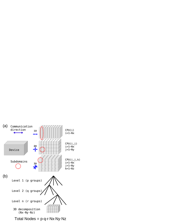
To reduce compute times by utilization of computers in excess of 10,000 cores, a new domain decomposition scheme is introduced in OMEN 3-D. In OMEN 3-D, a device of any shape can be spatially decomposed into three dimensions and each subdomain is assigned to corresponding processor. The maximum number of processors equals to the number of unit cells in each direction. Based on the spatial information, each processor only has the list of information of the atoms in its subdomain and neighbor atoms from adjacent subdomains; no global position infromation is held locally, minimizing the memory consumption and making it possible to simulate large devices (Fig.1(a)).
The major drawback for 3D parallelization is the increase of the complexity of communication by . The increased coupling among the processors may cause significant performance degradation; there is a trade-off between reducing the computational burden and increasing communication overhead. However, recent benchmark results indicated the average time consumed in the Message Passing Interface (MPI) communication is typically 5% of the total simulation time. Moreover, from the NEMO 3-D cases, it was shown that the total simulation time was not bound by communication as long as the ratio of the number of surface atoms to the total number of atoms in each subdomain is kept sufficiently small[13].
II-B Benchmark Results
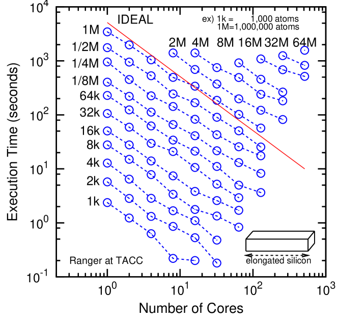
The strong scaling plot of the 500 Lanczos iterations using the basic 1-D parallelism for elongated systems of different number of atoms is presented in Fig. 2. This plot indicates that with minimal load of communication, OMEN 3-D shows reasonable scalability up to the structure that contains 32 million atoms with 512 processors in Ranger. However, with smaller number of atoms per subdomain, fluctuations in performance are observed as we increase the number of processors; this instability stems from the communication load being comparable to the computational operations.
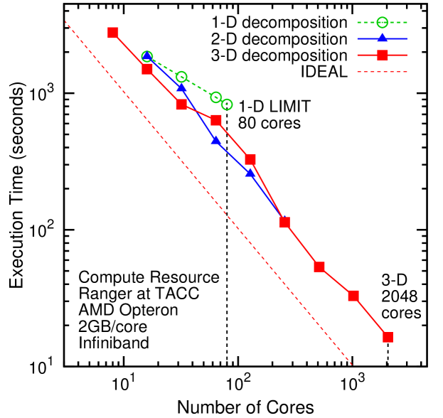
The strong scaling plot in Fig. 3 examines the performance of the 3-D decomposition scheme using 500 Lanczos iterations. The structure under test is a silicon cube, which has 4 million atoms (80 unit cells in each direction). As with the previous strong scaling result, 1-D decomposition scheme scales linearly; the number of processors can be assigned is limited to 80. On the other hand, 2-D and 3-D parallelization enables to assign more processors to the calculation, resulting in a proportional time reduction. It is measured in this example that the performance is enhanced by 13.3 times by using 16 times more processors. Therefore, by utilizing more computational resources, the 3-D decomposition scheme opens the possibility of delivering simulation results of realistic devices within significantly reduced time.
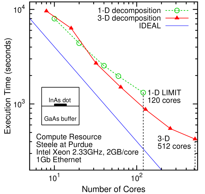
Typical NEMO 3-D simulations of InAs/GaAs Quantum Dot(QD) systems [11] not only involve electronic structure calculations but also require minimization of the total strain energy in an atomistic Valence Force Field (VFF) method [2]. This strain calculation is computationally significantly simpler than the subsequent electronic structure calculation. It therefore does not in general scale as well with increased parallelism. Here we test the VFF algorithm in 1D and 3D decomposition in OMEN 3-D (Fig. 4). The sample structure is a cylindrical InAs QD of size embedded in GaAs buffer, which is comprised of 13 million atoms. Again, 3-D decomposition scheme helps to scale down further to a factor of 3.5 by allocating 4 times more processors.
II-C Multi-Level Parallelism
OMEN 3-D also has a programmable interface ready for multi-level parallelism as depicted in Fig. 1 (b) to achieve extra performance enhancement. In contrast to the spatial domain decomposition, where the processors are coupled to each other by MPI communication, this hierarchical parallelism solves the task independently, with different parameters assigned for each group. K-space grouping, for example, can be useful when bandstructure or charge calculations are needed. Additional bias groups can be added for simulations that may involve external electrical or magnetic fields. Depending on the application, OMEN 3-D can provide multiple levels of additional parallelism to utilize more computational resources.
III Application
III-A The Schrödinger-Poisson Solver
One of the first applications of OMEN 3-D is the self-consistent charge and potential calculation module, known as the Schödinger-Poisson solver, which was not present in NEMO 3-D. There are three main components in the self-consistent loop:
-
1.
Schrödinger Equation Solver: Solves the eigenstates of the Schrödinger equation on finite k-points based on either tight binding or effective mass Hamiltonian using iterative eigenvalue solver, such as, (block) Lanczos or PARPACK.
-
2.
Charge Calculation: Based on the eigensolutions from the Schrödinger equation, there are two different approaches to obtain the charge profile. In the case of a given Fermi level, the charge profile can be calculated simply by filling up the states. On the other hand, if the Fermi level needs to be determined by external conditions, such as charge neutrality, both the charge and the Fermi level can be determined simultaneously.
-
3.
Poisson Solver: Charge is fed into the Poisson solver. The Poisson solver in OMEN 3-D also adopts 3-D parallelism and uses a finite difference method with the Aztec linear solver. The converged potential profile is iteratively obtained using Newton-Raphson’s method. The potential result is updated in the Hamiltonian and the steps are repeated until the self-consistency is achieved.
The Schrödinger-Poisson solver has been applied to a couple of physical simulations.
- •
- •
III-B Example: Bandstructure of the Phosphorus layers in silicon
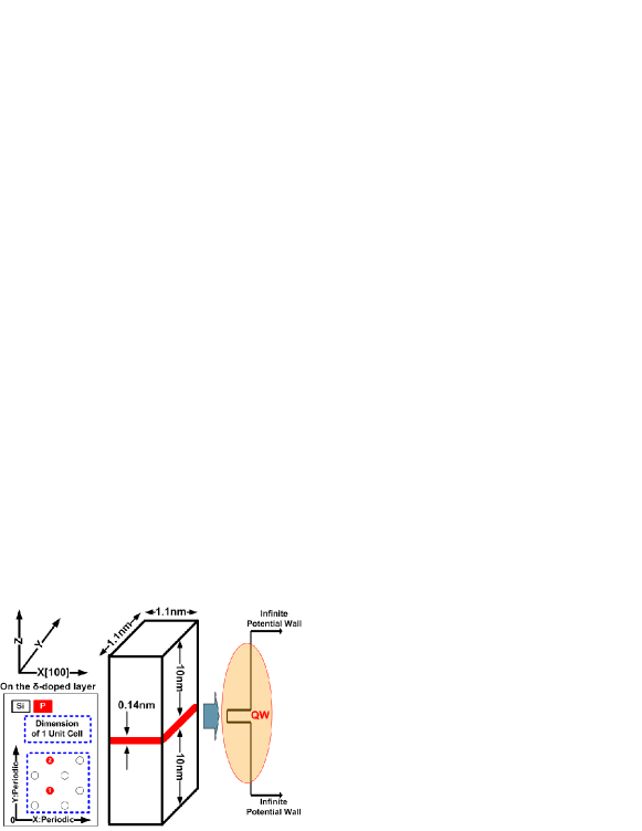
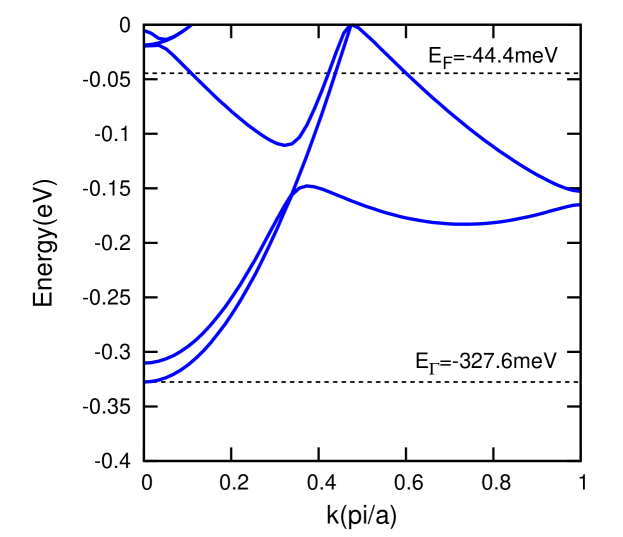
Advances in fabrication process has enabled the creation of atomic-scale devices in silicon. Using Scanning Tunneling Microscope (STM), experimentalists can fabricate phosphorus layers and encapsulate them in silicon [18]. This technology is significant in two fold; it is relevant in nanoelectronic device fabrication and it highlights the possibility of fabricating quantum computers. Using the self-consistent method, the bandstructure of the 2-D periodic layer structure with the doping density of 1/4 Mono Layer(ML) (Fig. 5) is calculated at T=4K. The bandstructure (Fig. 6) indicates that due to the potential induced by closely placed ionized donors, impurity bands are formed below the silicon bulk conduction band. The band minima and the Fermi level is located at 327.6meV and 44.4meV below the conduction band minima, respectively. For detailed simulation and analysis of the temperature dependence on Si:P layer, refer to reference [19].
IV Conclusion
The new nanoelectronic simulator OMEN 3-D is developed to overcome the limitations of NEMO 3-D in a processor-rich environment. The new parallel algorithm introduced in OMEN 3-D shows better scalability and is applicable to massive simulations and we expect to run further tests on several thousands of processors. This work will allow us to perform NEMO 3-D like calculations in minutes rather than days. As an example, the Schrödinger-Poisson module and its application to Si:P layer at 4K was introduced. Due to the potential formed by impurity ions, set of impurity bands are observed below the Si bulk conduction band. According to the simulation result, the Fermi level was located 44.4meV below the conduction band minima for 1/4ML Si:P layer.
Acknowledgment
NSF-funded nanoHUB.org and Ranger@TACC computational resources were used in this work. This work was supported by NSF, Purdue Research Foundation, and the Army Research Office. Discussions with Mathieu Luisier, Benjamin Haley and Abhijeet Paul are gratefully acknowledged.
References
- [1] G. Klimeck, F. Oyafuso, T.B. Boykin, R.C. Bowen and P. von Allmen, “Development of a Nanoelectronic 3-D(NEMO 3-D) Simulator for Multimillion Atom Simulations and Its Application to Alloyed Quantum Dots,” CMES Vol.3, No.5 pp.601-642,2002
- [2] G. Klimeck, S. Ahmed, H. Bae, N. Kharche, R. Rahman, S. Clark, B. Haley, S. Lee, M. Naumov, H. Ryu, F. Saied, M. Prada, M. Korkusinski and T.B. Boykin, “Atomistic Simulation of Realistically Sized Nanodevices Using NEMO 3-D:Part I-Models and Benchmarks,” IEEE Trans. Elec. Dev., Vol.54, Issue 9, pp2079-2089, Sept.2007
- [3] T.B. Boykin,G. Klimeck,R.C. Bowen and F. Oyafuso, “Diagonal parameter shifts due to nearest-neighbor displacements in empirical tight-binding theory,” Phys. Rev. B, 66, 125207, 2002
- [4] T.B. Boykin, G. Klimeck and F. Oyafuso, “Valence Band effective-mass expressions in the empirical tight-binding model applied to a Si and Ge parameterization,” Phys. Rev. B, 69, 115201, 2004
- [5] T.B. Boykin, N. Kharche and G. Klimeck, “Brillouin-zone unfolding of perfect supercells having nonequivalent primitive cells illustrated with a Si/Ge tight-binding parameterization,” Phys. Rev. B, 76, 035310, 2007
- [6] G. Klimeck, S. Ahmed, N. Kharche, M. Korkusinski, M. Usman, M. Prada and T.B. boykin, “Atomistic Simulation of Realistically Sized Nanodevices Using NEMO 3-D:Part II-Applications,” IEEE Trans. Elec. Dev., Vol.54, Issue 9, pp2090-2099, Sept.2007
- [7] S. Ahmed, N. Kharche, R. Rahman, M. Usman, S. Lee, H. Ryu, H. Bae, S. Clark, B. Haley, M. Naumov, F. Saied, M. Korkusinski, R. Kennel, M. McLennan, G. Klimeck, T.B. Boykin, “Multimillion Atom Simulations with NEMO 3-D,”Springer Encyclopedia for Complexity,Aug.2008
- [8] N. Kharche, M. Prada, T.B. Boykin and G. Klimeck, “Valley-splitting in strained silicon quantum wells modeled with 2 degree miscuts, step disorder and alloy disorder,” Applied Phys. Lett., 90, 092109, 2007
- [9] G.P. Lansbergen, R. Rahman, C.J. Wellard, I. Woo, J. Caro, N. Collaert, S Biesemans, G. Klimeck, L.C.L. Hollenberg and S. Rogge, “Gate-induced Quantum-confinement Transition of a Single Dopant Atom in a Silicon FinFET,” Nature Physics, 4, pp656-661, Aug.2008
- [10] G.P. Lansbergen, R. Rahman, C.J. Wellard, J. Carol, N. Collaert, S. Biesemans, G. Klimeck, L.C.L. Hollenberg and S. Rogge, “Transport-based Dopant Mapping in Advanced FinFETs,” IEEE IEDM, San Francisco, USA, Dec. 15-17, 2008
- [11] M. Usman, H. Ryu, I. Woo, D.S. Ebert and G. Klimeck, “Moving Towards nano-TCAD Multi-million Atom Quantum Dot Simulations Matching Experimental Data,” Accepted in IEEE Trans. on Nanotechnology, to appear in 2009
- [12] H. Bae, S. Clark, B. Haley, H. Ryu, G. Klimeck, S. Lee, M. Luisier and F. Saied, “A Nano-electronics Simulator for Petascale Computing: from NEMO to OMEN,” Proceedings of TeraGrid 2008, June 9-13, 2008, Las Vegas
- [13] http://cobweb.ecn.purdue.edu/gekco/nemo3D/index.html
- [14] N. Neophytou, A. Paul, M. Lundstrom and G. Klimeck, “Bandstructure Effects in Silicon Nanowire Electron Transport,” IEEE TED, Vol. 55, Issue 6, pp1286-1297, June 2008
- [15] A. Paul, S. Mehrotra and G. Klimeck, “Study of electronic charge distribution in silicon nanowire transistors: an atomistic approach,” APS March Meeting, March 16-20, Pittsburgh, PA, 2009
- [16] F.J. Reuss, B. Weber, K.E.J. Goh, O. Klochan, A.R. Hamilton and M.Y. Simmons, “One-dimensional conduction properties of highly phosphorus-doped planar nanowires patterned by scanning probe microscopy,” Phys. Rev. B, 76, 085403, 2007
- [17] F.J. Reuss, L. Oberbeck, M.Y. Simmons, K.E.J. Goh, A.R. Hamilton, T. Hallam,S.R. Schofield, N.J. Curson and R.G. Clark, “Toward Atomic-Scale Device Fabrication in Silicon Using Scanning Probe Microscopy,” Nano Letters, 4(10), pp 1969-1973, 2004
- [18] F.J. Reuss, W. Pok, K.E.J. Goh, A.R. Hamilton and M.Y. Simmons, “Electronic properties of atomically abrupt tunnel junctions in Silicon,” Phys. Rev. B, 75, 121303, 2007
- [19] H. Ryu, S. Lee and G. Klimeck, “A Study of Temperature-dependent properties of n-type -doped Si bandstructures in equilibrium,” Accepted in IWCE-13, IEEE proceedings, 2009