Ab initio vibrations in nonequilibrium nanowires
Abstract
We review recent results on electronic and thermal transport in two different quasi one-dimensional systems: Silicon nanowires (SiNW) and atomic gold chains. For SiNW’s we compute the ballistic electronic and thermal transport properties on equal footing, allowing us to make quantitative predictions for the thermoelectric properties, while for the atomic gold chains we evaluate microscopically the damping of the vibrations, due to the coupling of the chain atoms to the modes in the bulk contacts. Both approaches are based on the combination of density-functional theory, and nonequilibrium Green’s functions.
1 Introduction
Modeling charge transport in nanostructures under nonequilibrium conditions via ab initio methods is nowadays a well-established computational approach [1]. Electronic transport, however is intimately coupled to the motion of the ions comprising the nanostructure: the charges may excite ionic motion which leads to local heating and energy relaxation. On the other hand, the ionic motion itself is an important channel for heat transport between the electrodes. The vibrations within the nanostructure couple to the motion of the atoms in the bulk contacts, thus becoming damped or, equivalently, they obtain a finite life-time. The inelastic transport properties of nanostructures is a very active research field, where progress occurs on many fronts. In this paper we review two particular subfields in this general area. (i) We compute the ballistic electronic and thermal transport properties of Si-nanowires, paying specific attention to intentional nanostructuring. The main goal is to examine whether the thermoelectric properties can be enhanced via nanoengineering. Treating electronic and vibrational properties on equal footing (based on nonequilibrium Green’s functions) is a key element in our work. Presently it is not computationally feasible to consider inelastic scattering in these systems which typically consist of thousands of atoms. The important issue is thus to find a good compromise between microscopic accuracy, and the macroscopic properties of real, nanowire based devices. (ii) In smaller systems, such as the experimentally studied atomic gold wires, a fully microscopic approach has become tractable. The vibrational motion excited in the atomic chains due to electron transport is damped because the localized vibrations couple to the vibrations in the electrodes surrounding the gold chain. It is commonplace to describe this damping by phenomenological life-times; here, however, we describe a recently developed ab initio method to actually compute these life-times. Experimentally, a very rich behavior as a function of the elongation of the wire is observed, and the extreme sensitivity to stress, as revealed by our calculations, may form an important ingredient in explaining this behavior.
2 Ab initio modeling of electronic and thermal transport in Silicon nanowires (SiNW)
2.1 Background remarks
Recent ground-breaking experiments indicate that rough silicon nanowires (SiNWs) can be efficient thermoelectric materials although bulk silicon is not [2, 3]: they conduct charge well but have a low heat conductivity. A measure for the performance is given by the figure of merit , where , , and , are the electrical conductance, Seebeck coefficient, and (average) temperature, respectively. The heat conductivity has both electronic and phononic contributions, . Materials with are regarded as good thermoelectrics, but is required to compete with conventional refrigerators or generators [4]. Recent theoretical works predict in ultra-thin SiNWs [5, 6, 7]. The high performance SiNWs in Ref. [2] were deliberately produced with a very rough surface, and the high is attributed to increased phonon-surface scattering which decreases the phonon heat conductivity, while the electrons are less affected by the surface roughness. The extraordinary low thermal conductivity measured in rough SiNWs is supported by recent calculations [8, 9]. Surface disorder will, however, begin to affect the electronic conductance significantly in very thin wires [10] and thereby reduce [6, 7].
For defect-free wires, the room temperature phononic conductance scales with the cross-sectional area [11]. Contrary, for ultra-thin wires with diameters nm, the electronic conductance is not proportional to the area: it is quantized and given by the number of states at the band edges. Decreasing the diameter to this range thus decreases while keeping almost constant. An optimally designed thermoelectric material would scatter phonons but leave the electronic conductance unaffected, even for the smallest wires.
2.2 Optimizing the nanowire design
Instead of introducing surface disorder, which affects the electronic conductance in the thin wires, we have recently addressed the question whether other surface designs could lead to improved thermoelectric performance [12]. In a similar spirit, Lee et al. [13] proposed already earlier nanoporous Si as an efficient thermoelectric matrial. Blase and Fernández-Serra [14] have shown that covalent functionalization of SiNW surfaces with alkyl molecules leaves the electronic conductance unchanged, because the molecular states are well separated in energy from the nanowire bandedges, see Fig. 1. If the alkyl molecules scatter the phonons, such functionalized SiNWs would be promising candidates for thermoelectric applications. Experimental alkyl functionalization of SiNWs was reported in Ref. [15].
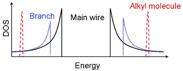
Another possible surface design are branched SiNWs, so-called nanotrees. Nanotrees have been synthesized in III-VI semiconductors [16, 17] and in silicon [18, 19]. The stability and electronic structure of silicon nanotrees have recently been addressed theoretically [20, 21]. The thinner branches will have a larger band gap than the main wire (”trunk”), see Fig. 1. Close to the band edges, the electronic scattering is therefore weak.
The presence of an alkyl molecule or a nanowire branch leads both to a reduction, , of the thermal conductance and a reduction, , of the electronic conductance. As we show in Ref. [12], at room temperature (RT) the ratio for the alkyl functionalized SiNWs, and for a nanotree. By engineering the SiNW surfaces it is thus possible to reduce the phonon conductance while keeping the electronic conductance almost unaffected. Such surface decorated SiNWs would be promising candidates for nanoscale thermoelectric applications.
2.3 Systems
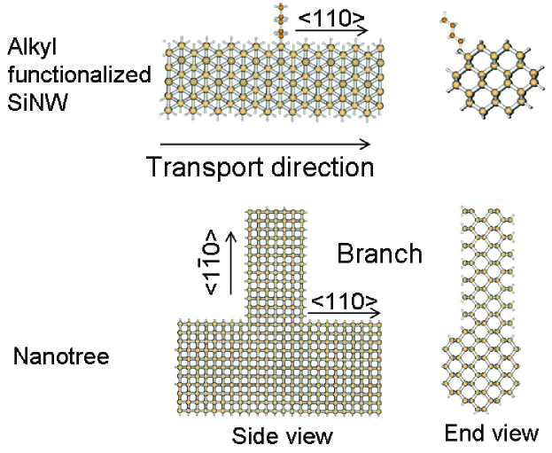
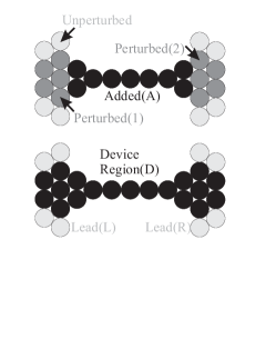
We consider two specific systems shown in Fig. 1. The first is an alkyl functionalized SiNW with a wire diameter of 12 Å, and with the wire oriented along the direction. The alkyl (CnH2n+1) is attached to the H-passivated nanowire replacing a H atom. The second system is a nanotree, where a small diameter (12 Å) branch is attached to a larger diameter (20 Å) trunk. The trunk is oriented in the direction while the branch is oriented along the direction, and is thus perpendicular to the trunk. The length of the branch, , is varied.
2.4 Methods
The electronic Hamiltonian, , and overlap matrix, , of the alkyl functionalized SiNWs are obtained from local orbital DFT calculations [22]. The calculations are performed on super-cells containing 7 wire unit cells, as indicated in Fig. 1.
For the nanotrees, we use a tight-binding (TB) model since these systems contain atoms, too many for our DFT implementation. The electronic TB Hamiltonian describing the nanotree is calculated using a 10 band nearest-neighbor orthogonal TB parametrization [23, 24]. We recently applied the same TB model to study thermoelectric properties of surface disordered SiNWs [7]. The same TB parameters were recently also applied to study SiNW band structures [25] and surface roughness [10, 26].
The phononic system is described using the Tersoff empirical potential (TEP) model [27, 28] for both the nanotree and the functionalized SiNW. For pristine wires, we have recently shown that the TEP model agrees well with more elaborate DFT calculations [11]. We limit our description to the harmonic approximation, thus neglecting phonon-phonon scattering. The harmonic approximation is always valid at low temperatures. In bulk Si, the room temperature anharmonic phonon-phonon relaxation length at the highest frequencies is nm and increases as at lower frequencies [29]. Experimental studies of silicon films [30] showed that the effective mean free path of the dominant phonons at room temperature is 300 nm. For relatively short wires with lengths nm the anharmonic effects thus seem to be of limited importance, and the harmonic approximation is expected to be good.
We calculate the electronic conductance from the electronic transmission function, following the standard non-equilibrium Green’s function (NEGF)/Landauer setup, where the scattering region (i.e. the regions shown in Fig. 1) is coupled to semi-infinite, perfect wires [31]. Explicitly, the transmission function is given by
| (1) |
where the retarded and advanced Green functions can be calculated recursively, and the coupling matrices are evaluated with a DFT calculation. A discussion of the validity of this expression can be found, e.g., in Ref.[31]. The electronic quantities in the formula can then be written as [32, 33, 34] , and where is given by
| (2) |
The phonon transmission function, , at frequency is calculated in a similar way as the electronic transmission with the substitutions ( is the force constant matrix) and , where is a diagonal matrix with the atomic masses [35, 36, 37]. The phonon thermal conductance is
| (3) |

2.5 Charge transport
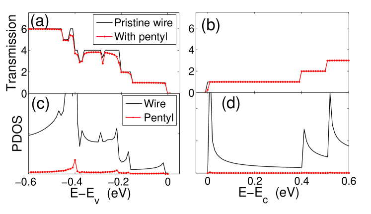
Figures 2 (a) and (b) show the calculated hole and electron transmissions for a pentyl (C5H11) functionalized SiNW. Notably, the transmission is nearly perfect close to the bandedges, in agreement with the findings of Ref. [14]. Figures 2 (c) and (d) show the projected density of states (PDOS) on the wire and on the pentyl. The high transmission regions in panel (a) and (b) are seen to correspond with regions of vanishing PDOS on the pentyl molecule. Likewise, at energies in the valence band where scattering is observed, there is a relatively large PDOS at the pentyl.
Figures 2 (e) and (f) show the transmission through the nanotree. The branch length is Å. Again, the transmission close to the band edges is nearly perfect. Figures 2 (g) and (h) show the PDOS on the main wire and on the branch. We again observe a correspondence between perfect transmission and low PDOS on the branch.
The almost perfect transmissions close to the band edges can be qualitatively understood from the schematic drawing in Fig. 1 (top). The HOMO and LUMO level of the pentyl are located deep inside the bands [14] and the molecular states are thus not accessible for electrons or holes close to the band edges. For the nanotree, the branch has a smaller diameter and thus a larger bandgap. Electrons or holes in the trunk, with energies close to the band edges, are not energetically allowed in the branch and therefore do not ’see’ the branch. In addition to the energy considerations, the spatial distribution of the Bloch state also plays a role: the first valence and conduction band Bloch states of the main wire have more weight in the center of the wire than at the edge [7].
2.6 Thermal transport
Figure 3 shows the temperature dependence of the thermal conductance ratios , where is the pristine wire thermal conductance, which in the low energy limit equals the universal thermal conductance quantum, [38]. Panel (a) shows the ratios for wires with alkyles, CnH2n+1, with different lengths, . The thermal conductance at RT is reduced by %, and the overall behavior does not depend on the alkyl length. The inset shows the phonon transmission at low phonon energies. Note the resonant dips in the transmission, where exactly one channel is closed yielding a transmission of three. These dips are associated with an increased local phonon density of states at the alkyl molecule at the resonant energies, corresponding to a localized vibrational mode. Such Fano-like resonant scattering is well-known from electron transport [39]. A phonon eigenchannel analysis [40] shows that the transmission dips are due to a complete blocking of the rotational mode in the wire. The corresponding localized alkyl phonon mode is a vibration in the plane perpendicular to the wire axis.
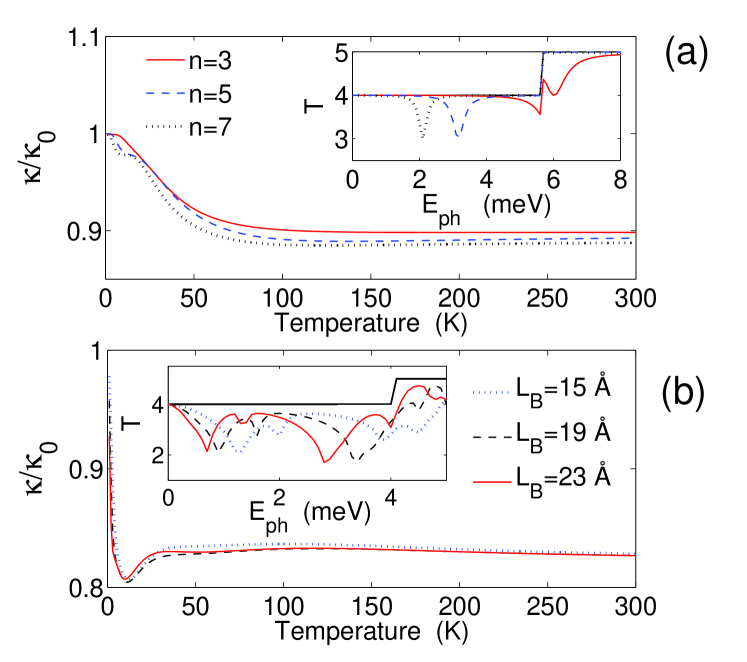
Panel (b) in Fig. 3 shows the thermal conductance ratio for nanotrees with different branch length, . There is only a weak dependence on at low temperatures, and at RT the four curves basically coincide showing a thermal conductance reduction of 17% of the nanotree compared to the pristine wire. Again we observe resonant transmission dips for the nanotrees. Two channels - the rotational and one flexural mode - close completely at the resonance due to two quasi-localized vibrational modes in the branch. These phonon backscattering resonances are responsible for the dip in the ratio around K. Notice that all the conductance ratios approach unity in the low temperature limit. This is because the four acoustic modes transmit perfectly in the limit [38].
We may vary the thermoelectric figure of merit, , by varying the chemical potential. Typically displays a maximum for close to the band edge [7, 5]. Figure 4 shows the maximum values for the pentyl functionalized SiNW (squares), the nanotree (circles), and surface disordered SiNWs (triangles), where disorder is modeled by introducing surface silicon vacancies. The diameter of the surface disordered wire is Å and it is oriented along the direction. The calculational details are given in Ref. [7]. The curves show as a function of the number () of pentyl molecules/nanotree branches/silicon vacancies.
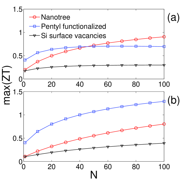
Figure 4 shows that increasing the number of scattering centers, i.e. the number of pentyl molecules or nanotree branches increases the for both hole transport (a) and electron transport (b). In the case of holes in the pentyl functionalized SiNWs, the reaches an almost constant level of at , but in all other cases increases throughout the range. Increasing the density of molecules/nanotree branches or increasing the length of the wire will thus increase the thermoelectric performance. The surface disordered wires (triangles) show an increasing vs but at values significantly lower than the two other surface modified wires.
2.7 Discussion
A number of idealizations have been made in our calculations, and we next assess their significance. The structures we have considered represent plausible choices, dictated by computational limitations, but do not necessarily match quantitatively real structures. Thus, for example, a surface decorated SiNW will also be rough, and one should consider the combined effect of all scattering mechanisms. We have not carried out optimizations neither with respect to the attached molecules nor with respect to the geometry of the nanotrees. Electron-phonon and phonon-phonon scattering will affect both the electronic and thermal conductances and the obtained values [6]. We do not expect to reach quantitative agreement with experiment but believe to have identified important trends: In SiNW based thermoelectrics, surface decorations in terms of added molecules or nanowire branches seem to be a better approach than surface disorder in the ultra-thin limit.
3 Microscopic theory for damping of vibrations in atomic gold wires
3.1 Introductory remarks
As pointed out in the beginning of this review, a particularly important issue in molecular electronics concerns the energy exchange between the charge carriers and the molecular contact. Thus, the local Joule heating resulting from the current passing through the contact, and its implications to the structural stability of such contacts are presently under intense investigation [41, 42, 43, 44, 45]. Experimentally, local heating in molecular conductors in the presence of the current has been inferred using two-level fluctuations [46] and Raman spectroscopy [47].
Mono-atomic chains of metal atoms [48] are among the simplest possible atomic-scale conductors. The atomic gold chain is probably the best studied atomic-sized conductor, and a great deal of detailed information is available from experiments and related theoretical studies; see Ref.[51] for an extensive list of references.
In the case of a gold chain Agraït et al.[50] reported well-defined inelastic signals in the current-voltage characteristics. These signals were seen as a sharp 1% drop of the conductance at the on-set of back-scattering due to vibrational excitation when the voltage equals the vibrational energy. Especially for the longer chains (6-7 atoms), the vibrational signal due to the Alternating Bond-Length (ABL) mode [52, 55], dominates. This resembles the situation of an infinite chain with a half-filled electronic band where only the zone-boundary phonon can back-scatter electrons [49] due to momentum conservation.
The inelastic signal gives a direct insight into how the frequency of the ABL-mode depends on the strain of the atomic chain. This frequency can also be used to infer the bond strength. The signature of heating of the vibrational mode is the non-zero slope of the conductance versus voltage beyond the on-set of excitation: with no heating the curve would be flat. Fits to the experiment on gold chains using a simple model [54] suggest that the damping of the excitation can be significant. However, the experiments in general show a variety of behaviors and it is not easy to infer the extent of localization of the ABL vibration or its damping in these systems111N. Agraït, private communication..
In order to address the steady-state effective temperature of the biased atomic gold chain theoretically, it is necessary to consider the various damping mechanisms affecting the localized vibrations, such as their coupling to the vibrations in the contact, or to the phonons in the surrounding bulk reservoirs. Here we outline how to calculate the vibrational modes in atomic gold chains and their coupling and the resulting damping due to the phonon system in the leads; a full account is available in our recent paper [59]. We work within the harmonic approximation and employ first principles density functional theory (DFT) for the atomic chain and the contacts [60] while a potential model is used for the force constants of the leads [61].
Here we focus on chains between two (100)-surfaces. We consider chain-lengths of 3-7 atoms and study the behavior of their vibrations and damping when the chains are stretched. TEM micrographs indicate that the chains are suspended between pyramids, so in our calculations we add the smallest possible fcc-stacked pyramid to link the chain to the given surfaces.
3.2 Method
In the microscopic modeling of the dynamics of the atoms forming the junction one must distinguish between different kinds of atoms: those belonging to the chain, those belonging to the pyramid joining the chain to the substrate, and substrate atoms. The technical issues of how these different types of atoms are treated are discussed in Ref.[59]. A quantity of central importance to all analysis is the mass-scaled dynamical matrix, K,
| (4) |
where is the total energy of the system, is the coordinate corresponding to the ’th degree of translational freedom for the atoms of the system. is the mass of the atom that the ’th degree freedom belongs to. K governs the the evolution of the vibrational system within the harmonic approximation. The Newton equation of motion reads
| (5) |
where denotes a mode of oscillation in the system and is the corresponding quantization energy. The evaluation of K proceeds as follows. Finite difference DFT calculations were used for the nanostructure, while for the surfaces we used an empirical model due to Tréglia and Desjonqu res [61]. The position of the interface between the region treated by DFT and the region treated by the empirical model is a parameter that can be varied; here one must find a value for which the physical results converge keeping the computational labor manageable.
3.3 Green’s functions projected on the atomic chain
All properties of interest in the present context can be derived from the Green’s function D,
| (6) |
where and we defined the inverse of the Green’s function by . Specifically, we shall need the Green’s function projected onto the region close to the atomic chain. Our procedure is based on a method due to Mingo et al.[62] which has previously been tested in an investigation of finite Si nanowires between Si surfaces. We find [59]
| (7) | |||||
where the index , i.e., the left and right unperturbed surface, while labels the regions in left contact, the atomic chain, and the right contact, that are different from the bulk (see Fig. 5). This expression defines the self-energy which has the matrix structure
| (8) |
This object can be evaluated as follows. First, in the limit of large regions 1 and 2, the coupling elements and must approach those of the unperturbed surface, and , respectively. In what follows, we shall make the approximation that the regions 1 and 2 are chosen so, that this condition is satisfied sufficiently accurately. Second, we note that the matrix is indistinguishable from the matrix , as long as the involved atoms are outside the perturbed regions 1 or 2. Therefore, we can write
where the accuracy increases with increasing size of regions 1 and 2. On the other hand, using the definition of the self-energy, we have
| (10) |
where is the projection of the unperturbed Green’s functions onto the atoms in regions 1,2, respectively. This object is evaluated by exploiting the periodicity in the ideal surface plane. The Fourier transform of in the parallel directions has a tridiagonal block structure and we can solve for its inverse very effectively using recursive techniques (see e.g. Sancho et al.[63]). An analysis of the convergence properties of this procedure is given in Ref.[59].
To sum up, the calculation is preformed in the following steps: (i) Start with perfect leads and specify the device in between them. (ii) The atoms in the leads where K is perturbed by the presence of the device are identified. (iii) The unperturbed surface Green’s function is found via -point sampling and then used to construct the self-energy, Eqs.(3.3–3.3). (iv) The perturbed Green’s function is then found using this self-energy via Eqs.(7–8). With the self-energy at hand, we can define the life-times of the various modes in a standard fashion (see Ref. [59] for details), and we now proceed to present some of our results.
4 Results
4.1 Geometrical Structure, the Dynamical Matrix, and Q-factors
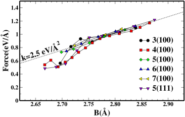
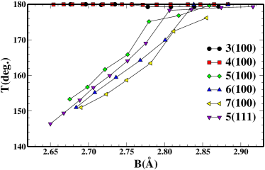
Here we report results for the geometrical structure of the chains as a function of the chain elongation. For each geometry (identified by the number of atoms in the chain, the surface orientation and the type of contact to substrate) a range of calculations were performed with the two surfaces at different separations, with the separations incremented in equally spaced steps. To be able to compare chains of different lengths and between different surfaces we define the average bond length, , as the average length between neighboring atoms within the chain, where runs over the number of bonds in the chain (see Fig. 6). is useful because it is closely related to the experimentally measurable force [51] on the chain. The close relationship between and the force is demonstrated in Fig. 7. We note that the force vs. curves to a good approximation follows a straight line with a slope of , which can be interpreted as the spring constant of the bonds in the chain.
As the systems are stretched it is mostly the bonds in the chain that are enlongated. At low Fig. 8 shows that the longer chains adopt a zig-zag confirmation at low average bond length. The 3- and 4-atom chains, however, remain linear within the investigated range. Furthermore, the longer chains have a similar variation in the average bond angle. Our results justify the earlier theoretical studies by Frederiksen et al.[55] and Sánchez-Portal et al.[64].
We next investigate the energies that are related to different types of movement by analyzing the eigenmodes and eigenvalues of selected blocks of K. In particular, we can consider the local motion of individual atoms or groups of atoms, freezing all other degrees of freedom, by picking the corresponding parts of K. The square root of the positive eigenvalues of the reduced matrix, which we call local energies, give the approximate energy of a solution to the full K that has a large overlap with the corresponding eigenmode, if the coupling to the rest of the dynamical matrix is low. The negative eigenvalues of a block are ignored since they correspond to motion that is only stabilized by degrees of freedom outside the block.
The behavior of the dynamical matrix in terms of local energies is illustrated in Fig. 9. In the chain the local energies are quickly reduced with increased strain while the dynamical matrix of the surfaces is hardly affected at all. The middle bonds in the chain are the ones that are strained and weakened most when the surfaces are moved apart. It is also where the chain is expected to break [65].
Fig. 10 shows how motion parallel to the chain occurs at higher energies than perpendicular motion, and that the LO type motion of the ABL modes has the highest energy. The local energies of the ABL/LO type motion move past the local energies of the pyramid as the strain is increased. In this way the ABL/LO modes can in some sense act as a probe of the contacts.
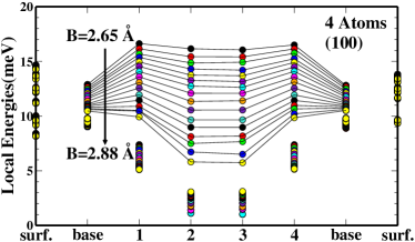
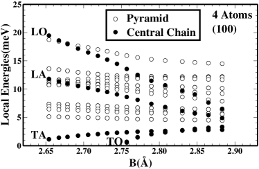
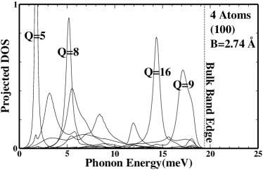
Figure Fig. 11 shows the projected DOS for a chain with 4 atoms at an intermediate strain. Notice the large variation in the width of the peaks. The peaks with a small width correspond to modes that have the largest amplitude in the chain, while the peaks with a large width correspond to modes with large amplitude on the interface.
In Fig. 12 we present the -factor, spatial localization and peak energy of all modes for chains with 3-7 atoms between (100) surfaces. The ABL modes are of special interest. These modes have been identified by previous theoretical and experimental studies as the primary scatterers of electrons[50, 52, 56, 53, 54, 57, 66]. The ABL modes are easily identified in Fig. 12 since they have the highest energy of the modes that are spatially localized to the central chain (black or dark gray on the figure). Modes corresponding to transverse motion of the central chain are also clearly visible. These modes are energetically and spatially localized, but are of limited interest because of a low electron-phonon coupling.
Certain ABL modes are very long-lived. At low strains, ABL modes lie outside the bulk (and surface) band and have, in the harmonic approximation, an infinite -factor. In reality the -factor will be limited by electron-phonon and anharmonic interactions. At higher strain the ABL modes move inside the bulk band and one observes a great variation in the corresponding -factors. When the peak energy lies inside the bulk band it will mostly be the structure of the connection between the bulk crystal and the chain that determines the width of the peak.
The long chains tend to have longer lived ABL/LO modes due to the larger ratio between the size of the chain and the size of its boundary. The 7-atom chain is especially interesting since it has an ABL/LO type mode with a damping of at one strain, while at another strain the ABL/LO mode has a damping of 300 meV, i.e., more than one order-of-magnitude variation in the harmonic damping of the primary scatterer of electrons due to only a 0.03 Å change in the average bond length!
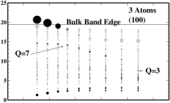
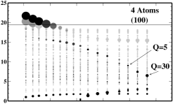
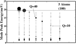
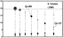
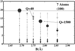
The largest damping of an ABL-mode for these systems is , which is still significantly lower than the band width. This can be attributed to fact, noted above, that there always exists a large mismatch in local energies moving from the central part of the chain to the rest of the system (see Fig. 9).
Previous studies by Frederiksen et al.[55] obtained a rough estimate for the variation of the non-electronic(harmonic and anharmonic) damping of 5-50 eV for the longer chains by fitting the experimental IETS signals of Agraït et al.[49] to a model calculation. The estimated peak energies lie well within the bulk band for all the recorded signals. The reason the non-electronic damping rate can be extracted is because the excitation of vibrations and damping of vibrations through electron-hole creation are both proportional to the strength of the electron-phonon coupling. This means that the step in the experimental conductance, when the bias reaches the phonon energy, can be used to estimate strength of the electron-phonon interaction and thereby the electron-hole pair damping. The slope in the conductance beyond this step can then be used to extract the total damping. By subtracting the electron-hole pair damping from the total damping we get an estimate of the sum of harmonic and anharmonic contributions to the damping.
The estimate in Ref. [55] agrees well with our lowest damping of 5 eV. The highest damping we have found was found for the 6 atom chain which is an order of magnitude larger than the upper limit of Ref. [55]. We believe that this discrepancy can be largely attributed to the difficulty in extracting the necessary parameters from experiments when the harmonic damping is large. Furthermore, for the 6-7 atom chains we observe that the high damping occurs at low strain, where the electron-phonon coupling is weak [49].
5 Conclusion and Discussion
Our most important finding is that the values of the harmonic damping for the ABL modes can vary by over an order of magnitude with strain. Even with small variations in the strain, the harmonic damping can exhibit this strong variation. This extreme sensitivity may explain the large variations seen experimentally in different chains.
The range of the harmonic damping also depends strongly on the number of atoms in the chain since we see a clear increase in localization going from a 6- to a 7-atom chain. The chain with 7 atoms really stands out, since it, in addition to having very localized modes in general, it also has the greatest variation in harmonic damping. This strong variation in the harmonic damping of the ABL/LO-modes suggests that accurate atomistic calculations of the vibrational structure is necessary to predict the inelastic signal.
The techniques described here can be combined with electronic transport calculations to predict the inelastic signal in the characteristic of a system. This will be done in future work, where we will also eliminate the use of the empirical model for the leads and use ab-initio parameters for the entire system.
We thank the Danish Center for Scientific Computing (DCSC) and Direktør Henriksens Fond for providing computer resources. The authors would like to thank Thomas Frederiksen for helpful discussions and Nicolas Agraït showing his unpublished experimental results. TM acknowledges the Denmark-America foundation for financial support. APJ is grateful to the FiDiPro program of the Finnish Academy.
References
References
- [1] M. Brandbyge et al., Physical Review B 65, 165401 (2002).
- [2] A. Hochbaum et al., Nature (London) 451, 163 (2008).
- [3] A. I. Boukai et al., Nature (London) 451, 168 (2008).
- [4] A. Marjumdar, Science 303, 777 (2004).
- [5] T. T. M. Vo et al., Nano Lett. 8, 1111 (2008).
- [6] E. Ramayya et al., Nano 08, 8th IEEE Conference on Nanotechnology, 339–342 (2008).
- [7] T. Markussen, A.-P. Jauho, and M. Brandbyge, Phys. Rev. B 79, 035415 (2009).
- [8] P. Martin et al., Phys. Rev. Lett. 102, 125503 (2009).
- [9] D. Donadio and G. Galli, Phys. Rev. Lett. 102, 195901 (2009).
- [10] M. P. Persson et al., Nano Lett. 8, 4146 4150 (2008).
- [11] T. Markussen, A.-P. Jauho, and M. Brandbyge, Nano Lett. 8, 3771 (2008).
- [12] T. Markussen, A.-P. Jauho, and M. Brandbyge, Phys. Rev. Lett. 103, 055502 (2009).
- [13] J.-H. Lee, G. A. Galli, and J. C. Grossman, Nano Letters 8, 3750 (2008).
- [14] X. Blase and M.-V. Fernández-Serra, Phys. Rev. Lett. 100, 046802 (2008).
- [15] H. Haick et al., J. Am. Chem. Soc. 128, 8990 (2006).
- [16] K. A. Dick et al., J. Cryst. Growth 272, 131 (2004a).
- [17] K. A. Dick et al., Nat. Mater. 3, 380 (2004b).
- [18] L. Fonseca, O. Resto, and F. Sola, Appl. Phys. Lett. 87, 113111 (2005).
- [19] G. S. Doerk et al., J. Mat. Chem. 18, 5376 (2008).
- [20] M. Menon et al., J. Comput. Theor. Nanosci. 4, 252 (2007).
- [21] P. V. Avramov et al., Nano Lett. 7, 2063 (2007).
- [22] J. M. Soler et al., J. Phys.: Condens. Matter 14, 2745 (2002).
- [23] T. B. Boykin, G. Klimeck, and F. Oyafuso, Phys. Rev. B 69, 115201 (2004).
- [24] Y. Zheng et al., IEEE Trans. Electron Devices 52, 1097 (2005).
- [25] Y. M. Niquet et al., Phys. Rev. B 73, 165319 (2006).
- [26] M. Luisier, A. Schenk, and W. Fichtner, Appl. Phys. Lett. 90, 102103 (2007).
- [27] J. Tersoff, Phys. Rev. B 38, 9902 (1988).
- [28] J. Tersoff, Phys. Rev. B 39, 5566 (1989).
- [29] N. Mingo and L. Yang, Phys. Rev. B 68, 245406 (2003).
- [30] Y. S. Ju and K. E. Goodson, Appl. Phys. Lett. 74, 3005 (1999).
- [31] H. Haug and A.-P. Jauho, Quantum Kinetics in Transport and Optics of Semiconductors, vol. 123 of Springer Solid State Series (Springer, 2008), 2nd ed.
- [32] U. Sivan and Y. Imry, Phys. Rev. B 33, 551 (1986).
- [33] K. Esfarjani, M. Zebarjadi, and Y. Kawazoe, Phys. Rev. B 73, 085406 (2006).
- [34] A. M. Lunde and K. Flensberg, J. Phys.: Condens. Matter 17 (2005).
- [35] T. Yamamoto and K. Watanabe, Phys. Rev. Lett. 96, 255503 (2006).
- [36] N. Mingo, Phys. Rev. B 74, 125402 (2006).
- [37] J.-S. Wang, J. Wang, and N. Zeng, Phys. Rev. B 74, 033408 (2006).
- [38] K. Schwab et al., Nature (London) 404, 974 (2000).
- [39] J. U. Nockel and A. D. Stone, Phys. Rev. B 50, 17415 (1994).
- [40] M. Paulsson and M. Brandbyge, Phys. Rev. B 76, 115117 (2007).
- [41] G. Schulze et al., Physical Review Letters 100, 136801 (2008).
- [42] Y. Teramae et al. Applied Physics Letters 93, 083121 (2008).
- [43] Z. F. Huang et al. Nature Nanotechnology 2, 698 (2007).
- [44] M. Galperin et al. Physical Review B 75, 155312 (2007).
- [45] D. A. Ryndyk et al. Physical Review B 78, 085409 (2008).
- [46] M. Tsutsui et al. Nano Letters 8, 3293 (2008a).
- [47] Z. Ioffe et al. Nature Nanotechnology 3, 727 (2008).
- [48] G. Rubio-Bollinger et al. Phys. Rev. Lett. 87, 026101 (2001).
- [49] N. Agraït et al. Chemical Physics 281, 231 (2002a).
- [50] N. Agraït et al. Physical Review Letters 88, 216803 (2002b).
- [51] N. Agraït, A. L. Yeyati, and J. M. van Ruitenbeek, Physics Reports 377, 81 (2003).
- [52] T. Frederiksen et al. Physical Review Letters 93, 256601 (2004), ISSN 0031-9007.
- [53] J. K. Viljas et al. Physical Review B 72, 245415 (2005).
- [54] M. Paulsson, T. Frederiksen, and M. Brandbyge, Physical Review B 72, 201101(R) (2005).
- [55] T. Frederiksen et al. Physical Review B 75, 205413 (2007a), ISSN 1098-0121.
- [56] T. Frederiksen et al. Physical Review B 75, 235441 (2007b), ISSN 1098-0121.
- [57] E. Hobi, A. Fazzio, and A. J. R. da Silva, Physical Review Letters 100, 056104 (2008).
- [58] M. Tsutsui, S. Kurokawa, and A. Sakai, Nanotechnology 17, 5334 (2006), ISSN 0957-4484.
- [59] M. Engelund, M. Brandbyge, and A. P. Jauho, Phys. Rev. B 80, 045427 (2009).
- [60] J. M. Soler et al. Journal of Physics: Condensed Matter 14, 2745 (2002).
- [61] G. Tréglia and M. C. Desjonquéres, Journal de Physique 46, 987 (1985).
- [62] N. Mingo et al. Physical Review B 77, 033418 (2008).
- [63] M. P. L. Sancho, J. M. L. Sancho, and J. Rubio, Journal of Physics F-Metal Physics 14, 1205 (1984).
- [64] D. Sánchez-Portal et al. Phys. Rev. Lett. 83, 3884 (1999).
- [65] P. Velez, S. A. Dassie, and E. P. M. Leiva, Chemical Physics Letters 460, 261 (2008).
- [66] J. Hihath et al. Nano Letters 8, 1673 (2008).