Radiation-induced quantum interference in low-dimensional - junctions
Abstract
We predict and analyze radiation-induced quantum interference effect in low-dimensional - junctions. This phenomenon manifests itself by large oscillations of the photocurrent as a function of the gate voltage or the frequency of the radiation. The oscillations result from the quantum interference between two electron paths accompanied by resonant absorption of photons. They resemble Ramsey quantum beating and Stueckelberg oscillations well-known in atomic physics. The effect can be observed in one- and two-dimensional - junctions based on nanowires, carbon nanotubes, monolayer or bilayer graphene nanoribbons.
pacs:
03.67.-a, 05.60.Gg, 72.80.Vp, 73.40.LqAlthough quantum mechanics was born more than a century ago, only in the last decades it became possible to manipulate in a coherent way the states of single discrete-level systems. Such fundamental phenomena as microwave-induced Rabi oscillations Rabi and Ramsey quantum beating Ramsey , which are well known in atomic physics and in principle can be realized in any two-level system, were observed recently in solid-state devices, for example, in Josephson qubits VionMartinis , quantum dots Kouwenhoven , and ferromagnetic domain walls Nowack . In order to manipulate quickly the states of a macroscopic system one normally applies a time-dependent perturbation, e.g. irradiates the system by an electromagnetic field (EF), with the frequency close to the splitting between respective energy levels. Time-dependent coherent phenomena in solid-state systems are observed traditionally in zero-dimensional systems, such as quantum dots or qubits.
Remarkably, the states of moving electrons in a two-band semiconductor can be handled by means of external radiation analogously to those of a two-level system. Indeed, if an electron propagates in a semiconductor in presence of a non-uniform potential, then its momentum is coordinate-dependent, and so is the splitting between the energies in the conduction and the valence bands. The interaction of the electron with the radiation occurs effectively only in the “resonant regions”, near the points where the resonant condition
| (1) |
is satisfied, being the photon energy. The transmission of an electron through a narrow resonant region is equivalent in its reference frame to the application of a short resonant pulse, which can coherently transfer the electron from one band to another. Electron states in the conduction and the valence band play here the same role as the two states of a two-level system (a qubit) subject to an EF. The coordinate-dependent potential and the distribution function of the incident electrons determine the effective time of the resonant interaction with the EF and the initial state of the qubit respectively.
For a particular example of graphene - junctions, the electron motion can be considered as the dynamical Landau-Zener tunneling through the dynamical gap opened in the electron spectrum by the resonant interaction with the EF FEprl ; SFEprb . Varying the frequency and the intensity of applied EF one can suppress transport in the junction FEprl ; SFEprb or generate photocurrent, the directed current flowing without any dc bias applied SFEprb . The opening of the dynamical gap and some of its effects on the classical bulky properties of semiconductors have been studied since quite a while ago GGE .
Although the dynamical gap bears a remarkable resemblance to the Rabi frequency Rabi ; Hanggi , observed routinely in experiments with two-level systems VionMartinis ; Kouwenhoven ; Nowack , there is no obvious way to vary the time of resonant interaction of electrons with EF, and the coherent quantum-mechanical transport phenomena in low-dimensional - junctions have not been studied yet. However, the transmission of electrons through the resonant regions is equivalent to the dynamics of a two-level system subject to a sequence of resonant pulses. Thus, one may anticipate certain manifestations of Ramsey oscillations Ramsey in the transport properties of semiconducting junctions.
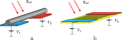
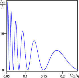
In this Letter we predict and analyze the effect of the radiation-induced quantum interference on the ballistic transport in low-dimensional - junctions. We show that the quantum interference leads to large oscillations of the photocurrent as a function of the difference of the gate voltages (cf. Fig. 1). The dependence is shown in Fig. 2 and has a universal form; the parameters of the system and the radiation determine only the amplitude and period of oscillations. The effect is rather strong in 1D semiconducting systems, such as nanowires, carbon nanotubes (CNTs) (Fig. 1a), or graphene nanoribons (GNRs) (Fig. 1b), but can also be observed in some 2D system, e.g. based in monolayer or bilayer graphene.
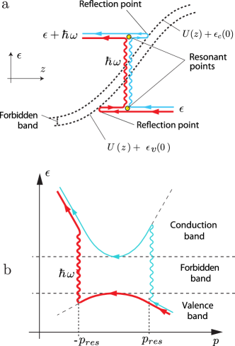
The oscillations of the photocurrent can be understood qualitatively as follows. The transmission of electrons through the junction is determined by two processes, namely, by the resonant absorption of photons near the “resonant points”, where the condition (1) is satisfied, and by the strong reflection from the junction interface, occurring at the “reflection points”, where the longitudinal component of momentum ( is the direction perpendicular to the interface) turns to zero. The resulting electron trajectories, which contribute to the photocurrent, are shown in Fig. 3. As one can see, there are two paths corresponding to the propagation from the right to the left: on the first one electrons move in the valence band between the resonant and the reflection points [red (black) line in Fig. 3], while on the second one analogous motion occurs in the conduction band [blue (gray) line in Fig. 3]. The interference between these two paths results in the oscillating dependence of the photocurrent on the gate voltages or on the frequency of the EF.
Let us present the quantitative analysis of the radiation-induced interference. The Hamiltonian of a 1D two-band semiconductor in presence of external EF and the coordinate-dependent potential reads
| (2) |
Here are the Pauli matrices, and is the matrix element of the resonant interband transitions, that depends on the intensity of the EF (), on its polarization, and on the type of the semiconducting material. The potential profile of the junction can be tuned by applying the gate voltages, Fig. 1. For simplicity we disregard electron spins and assume that there is only one valley.
It is convenient to carry out the calculations in the basis of electron eigenstates, which are related to the initial ones by the unitary transformation . The respective transformed Hamiltonian contains static parts and those proportional to . Similarly to the generic case of a two-level system, one can use the rotating-wave approximation (RWA) Hanggi , i.e. neglect the latter parts of the Hamiltonian near the resonance. Thus, we obtain the effective Hamiltonian
| (3) |
The same procedure has been used to analyze the electron transport in a graphene monolayer FEprl ; SFEprb and spin-dependent transport in a 2D electron gas FEspin . The RWA is valid as long as the amplitude of the EF is sufficiently small, . In the absence of the coordinate-dependent potential the eigenvalues of read
| (4) |
The Eq. (Radiation-induced quantum interference in low-dimensional - junctions) shows that the resonant interaction of electrons with EF opens the dynamical gap in the electron spectrum at the resonant momentum satisfying condition (1).
Let us proceed to the analysis of electron dynamics in presence of the coordinate-dependent potential . The classical phase trajectories of the Hamiltonian are determined by the energy conservation law:
| (5) |
where is the electron energy in the transformed basis, related to that in the initial basis as in the conduction (valence) bands far from resonant points.
Electron transmission through the resonant regions is determined by the tunneling through the dynamical gap , analogously to that through the forbidden band of conventional semiconductors TunnKadig or to the transmission of electrons through a graphene - junction Falko ; NovGeim . The position of the resonant point is determined by the condition
| (6) |
and Eq. (1). Approximating the potential in the vicinity of the the point by a linear function, one can describe the transmission through the resonant region by the Landau-Zener tunneling SFEprb ; FEprl . The tunneling probability reads
| (7) |
where is the slope of the potential close to the resonant point, and
| (8) |
The reflection from the resonant region, that occurs with probability , corresponds to the processes of the photon emission (absorption) in the initial basis of electron states. The reflection is accompanied by the velocity reversal (cf. Fig. 3a).
Far from the resonant point electrons weakly interact with the EF. The resulting classical trajectories in a smooth potential are shown in Fig. 3. As we mentioned before, there are two paths allowing the penetration from the right to the left. The total probability of the inelastic electron transmission reads
| (9) |
where are the quantum-mechanical phases along the two paths (cf. Fig. 3). The accumulated phase difference is
| (10) |
Here we assume for simplicity that the potential slope is constant in a sufficiently large region close to the - interface. In this case the phase is independent of the energy . Eq. (10) is the leading-order quasiclassical contribution to the phase difference; using it we neglect certain contributions of order unity that can result only in the shift of the oscillations of the photocurrent.
The current through the junction is given by the modified Landauer formula, allowing for the photon emission/absorption Moskaletz ; SFEprb :
| (11) |
Here and are the distribution functions in the left and the right leads, - the probability to penetrate from the right to the left lead accompanied by the energy change from to , - the number of the degrees of freedom not affecting the transport, e.g. spins, valleys, transverse channels. Taking into account that each electron in the energy interval in the valence band can absorb a photon and penetrate into the conduction band, we obtain the photocurrent as
| (12) |
Since the phase difference depends on the electric field , where is the length of an - junction, the photocurrent displays oscillations as a function of the gate voltages, i.e. of . The oscillations result from the quantum interference of electron moving in the confined area between the resonant and reflection points in the conduction and the valence bands (see Fig. 3). These oscillations are similar to the Stueckelberg oscillations Stueckelberg , the quantum interference effect occurring in quantum collisions due to the superposition of two quantum-mechanical pathways. If considered in the reference frame of moving electrons, the oscillations of the photocurrent bear resemblance to the “Ramsey fringes”, the quantum beating in the population of a two-level system subject to a sequence of resonant pulses. Indeed, introducing the period of electron motion in the conduction band as and the average kinetic energy of confined electrons, we write the phase difference as , and one can recognize the well-known parameter determining the period of “Ramsey fringes” Ramsey ; VionMartinis .
Let us apply our generic result, Eq. (12), to a particular case of - junctions based on GNRs and CNTs. These quasi-1D objects can be metallic or semiconducting. However, as their gapless modes do not contribute to the photocurrent, we can consider at sufficiently low frequencies the effective two-band spectrum Grnanotubes ; Tubes
| (13) |
The gap appears due to the transverse momentum quantization. Calculating the integral over in Eq. (10) with the spectrum (13) we arrive at the dependence of the photocurrent on the gate voltage (for ):
| (14) |
The parameters and determine respectively the amplitude and the period of the oscillations. The typical dependence on is shown in Fig. 2.
In order to observe the quantum oscillations in the photocurrent a few conditions are to be satisfied. The photon energy must exceed the width of the forbidden band . At the same time, to maximize the effect, should be sufficiently small not to involve in the transport any higher bands, and the forbidden band has to be large enough, to ensure a strong reflection from the junction interface. The gate voltage difference should be sufficient, , to create a smooth potential profile with a nearly constant slope close to the interface. The order of magnitude of the energy gap can vary from in strained metallic carbon nanotubes to in semiconducting CNTs or in GNRs Tubes , so the desired radiation frequency may be in the THz or in the infrared optical region. For example, for the typical junction parameters , , and for the radiation frequency , the characteristic scale (cf. Fig. 2) estimates . Thus, one can observe a large number of oscillations at .
Since the oscillations of the photocurrent is a coherent quantum interference effect, they can be destroyed by disorder and inelastic processes. For a good visibility of the oscillations the characteristic time of electron propagation between the resonant and the reflection points should be smaller than the scattering time, i.e. . On the other hand the deviation of the dependency from the universal form [Eq. (14)] allows one to quantitatively analyze the processes of elastic and inelastic scattering in such systems.
The oscillations can be observed in some 2D - junctions as well, for example, in those based on bilayer graphene. Electrons there have a quadratic two-band spectrum , which leads to the strong reflection from the - interface NovGeim ; Blanter and thus allows one to confine electrons between the resonant and reflection points, as necessary for observing the oscillations. Their characteristic period is with . In systems the phase depends on the transverse momentum , . As a result, the oscillations of the photocurrent are smeared and suppressed by the parameter , as compared to the 1D case.
In conclusion, we predict and analyze radiation-induced quantum interference effect in the dc transport properties of low-dimensional - junctions subject to an externally applied EF. This phenomenon manifests itself by large oscillations in the dependence of the photocurrent on the gate voltage or on the frequency of the EF. The effect can be observed in diverse quasi-1D semiconducting systems, such as nanowires, carbon nanotubes (CNTs), or graphene nanoribons (GNRs), as well as in some 2D system, e.g. bilayer graphene.
We are grateful to L.S. Levitov for useful discussions and to SFB 491, SFB Transregio 12, and the European Commission (FP7-ICT-2007-C; project No. 225955 STELE) for the financial support.
References
- (1) I. I. Rabi, Phys. Rev. 51, 652 (1937).
- (2) N. F. Ramsey, Phys. Rev. 78, 695 (1950).
- (3) D. Vion et al, Science 296, 886 (2002); J.M. Martinis, S. Nam, J. Aumentado, and C. Urbina, Phys. Rev. Lett. 89, 117901 (2002).
- (4) F. H. L. Koppens et al, Phys. Rev. Lett. 99, 106803 (2007)
- (5) K. C. Nowack et al, Science 318, 1430 (2007).
- (6) M. V. Fistul and K. B. Efetov, Phys. Rev. Lett. 98, 256803 (2007).
- (7) S. V. Syzranov, M. V. Fistul, and K. B. Efetov, Phys. Rev. B 78, 045407 (2008).
- (8) V. M. Galitskii, S. P. Goreslavskii, and V. F. Elesin, Sov. Phys. JETP 30, 117 (1970)
- (9) P. Hänggi, in Quantum Transport and Dissipation edited by T. Dittrich, P. Hänggi, G-L. Ingold, B. Kramer, G. Schön and W. Zwerger, Wiley-VCH, Weinheim (1998).
- (10) M. V. Fistul and K. B. Efetov, Phys. Rev. B 76, 195329 (2007).
- (11) E. O. Kane and E. I. Blount, in Tunneling Phenomena in Solids, edited by E. Burstein and S. Lundqvist, Plenum Press, N. Y. (1969); A. A. Slutskin and A. M. Kadigrobov, Sov. Phys. Solid State, 9, 138 (1967).
- (12) V. V. Cheianov and V. I. Fal’ko, Phys. Rev. B 74, 041403(R) (2006); A. V. Shytov, N. Gu, and L. S. Levitov, arXiv e-prints (2008), 0708.3081.
- (13) K. S. Novoselov, et. al., Nature 438, 197 (2005).
- (14) M. Moskalets and M. Büttiker, Phys. Rev. B 66, 205320 (2002).
- (15) E. C. G. Stueckelberg, Helv. Phys. Acta 5, 369 (1932).
- (16) M. Y. Han et al, Phys. Rev. Lett. 98, 206805 (2007).
- (17) Z. F. Wang et al, Applied Physics Letters, 91, 053109 (2007); C. T. White, D. H. Robertson, and J. W. Mintmire, Phys. Rev. B 47, 5485 (1993).
- (18) E. McCann, D. S. I. Abergel, V. I. Falko, Solid State Communication, 143, 110 (2007); Ivar Martin, Ya. M. Blanter, and A. F. Morpurgo, Phys. Rev. Lett. 100, 036804 (2008)