Evidence of gate-tunable topological excitations in two-dimensional electron systems
Abstract
Topological defects are ubiquitous from solid state physics to cosmology, where they drive phase transitions by proliferating as domain walls, monopoles or vortices. As quantum excitations, they often display fractional charge and anyonic statistics Laughlin , making them relevant to topologically protected quantum computation Nayak , but realizing a controlled physical resource for topological excitations has been difficult. Here we report evidence of topological excitations during the localization transition in strongly interacting two-dimensional electron systems (2DESs) in GaAs/AlGaAs heterostructures. We find the electrical conductivity at low electron densities to follow a Berezinskii-Kosterlitz-Thouless (BKT)-like order-disorder transition implying a gate-tunable proliferation of charged topological defects Berezenskii ; KT . At low temperatures, a weakening in the temperature dependence of conductivity was observed, and linked to the zero point fluctuations and delocalization of the defects. Our experiments also cast crucial insight on the nature of the ground state in strongly interacting 2DESs in presence of disorder
At low temperatures (), electrical conductivity of a disordered 2DES decreases rapidly when the carrier density is reduced. The dependence of on often reflects the nature of the ground state which is electrically insulating. A classical percolation transition in inhomogenous 2DESs, for example, would cause to vary as for , where is the carrier density at the percolation threshold Sarma . When disorder decreases, transition to the insulating state occurs at much lower , where the inter-particle Coulomb interaction is strong, and corresponds to a large interaction parameter ( is the effective Bohr radius). The nature of the ground state in an interacting 2DES is far from clear, although possibilities of pinned charge-density waves (CDW), such as a Wigner crystal Tanatar ; Tsui ; PD ; Camjayi ; Eguiluz , charge stripes Murthy ; Koulakov , or other phases Kivelson , have been suggested frequently. Physics of 2DES in this regime offers exotic possibilities such as metallic ground states, diverging effective mass and -factors, and so on Camjayi .
In 2D, a CDW state with long range order does not exist at finite . However, states with quasi-long range order can exist, which can then undergo phase transitions into a disordered states through BKT type transitions involving the proliferation of topological defects Berezenskii ; KT ; Thouless ; Halperin ; Young ; Fertig . Such transitions can in principle be effected by varying or , and the correlation length () in the disordered state is a non-analytic function of the distance from the phase boundary in density and temperature space:
| (1) |
where is a constant, and or . When , topological defects unbind, resulting in finite conductivity in the otherwise insulating pinned CDW state. The conductivity varies in accordance with the number density () of these defects, although an explicit evidence of this has not been observed until recently Ong .
2DESs in modulation-doped GaAs/AlGaAs heterostructures are excellent testing ground for many-body physics, because it allows great control on the level of disorder. Similar to transverse magnetic field () PD , disorder can also stabilize CDW state, even in the absence of , by suppressing the long wavelength fluctuations and arresting the kinetic energy of the electrons Eguiluz . This increases the melting point (i.e. and ), but excessive disorder may limit the order to very short range, or produce a glassy state, highlighting the need for a subtle balance. We use Si-doped GaAs/AlGaAs heterostructures, where disorder arises from (1) Coulomb potential of ionized Si-atoms, and (2) unintentional background doping. The former component was tuned by using devices from wafers with different setback distances () between the dopants and the hetero-interface (See Fig. 1a and Methods). It is important to prevent the device from pinching off (i.e. turn insulating) at high which is the case in macroscopic systems with inhomogenous charge distribution Tripathi ; Hamilton . Mesoscopic 2DESs are more suitable since they are relatively insensitive to long range fluctuations in the conduction band MBprb ; MBprl , and hence form the backbone of our experiments.
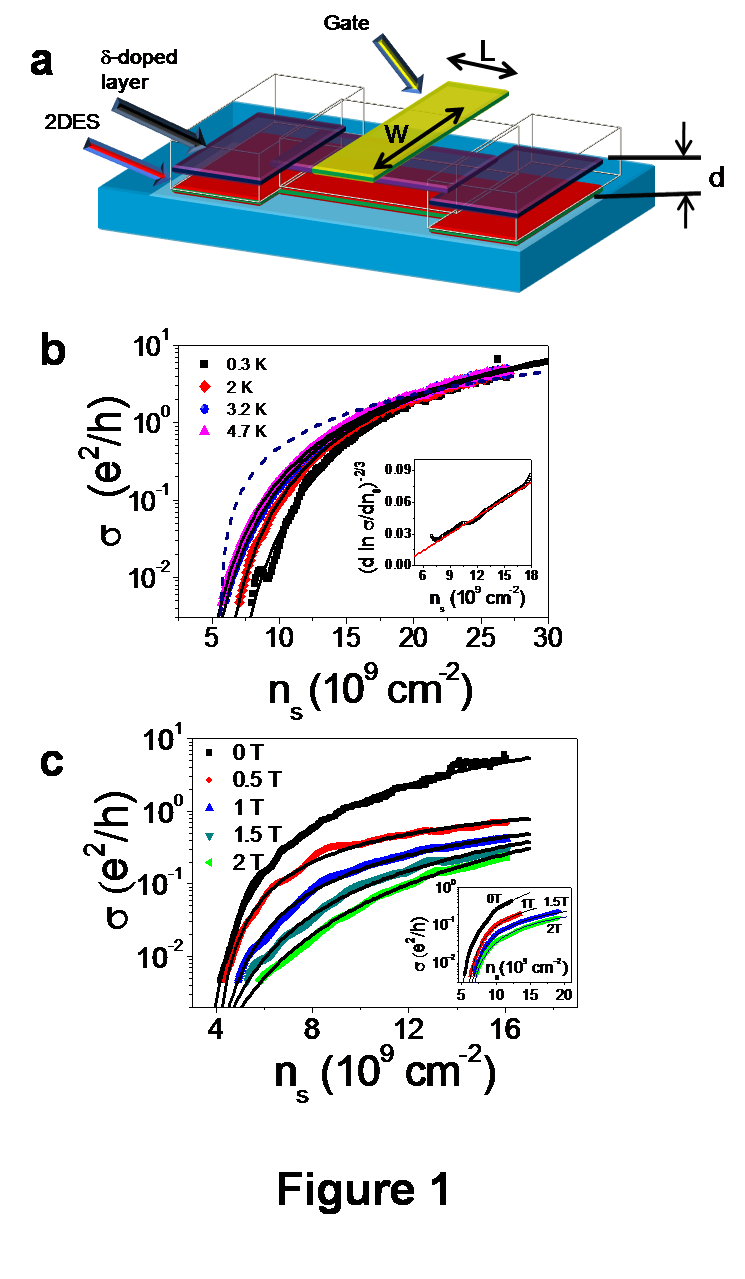
The devices were patterned in the form of a microbridge with a crossed metallic surface gate (Fig. 1a) (Ref [22]), limiting the effective area of the device to width of m and length m. With decreasing (negative potential on the gate), dropped rapidly in all devices, as illustrated in Fig. 1b and c. At low ( K), small modulations on overall smooth variation of were observed occasionally, which were not reproducible on thermal cycling. Moreover, a percolation transition also failed to describe the -dependence of in our devices (dashed line in Fig. 1b), indicating the influence of inhomogeneity to be small and sporadic. The pinch-off density where , decreases with increasing (shown in Fig. 1b for device C2367), but increases with increasing (shown in Fig. 1c for T546 and A2678). The density scale at which pinch-off occurs can be very low, cm-2, corresponding to , and hence the possibility of a CDW ground state arises naturally.
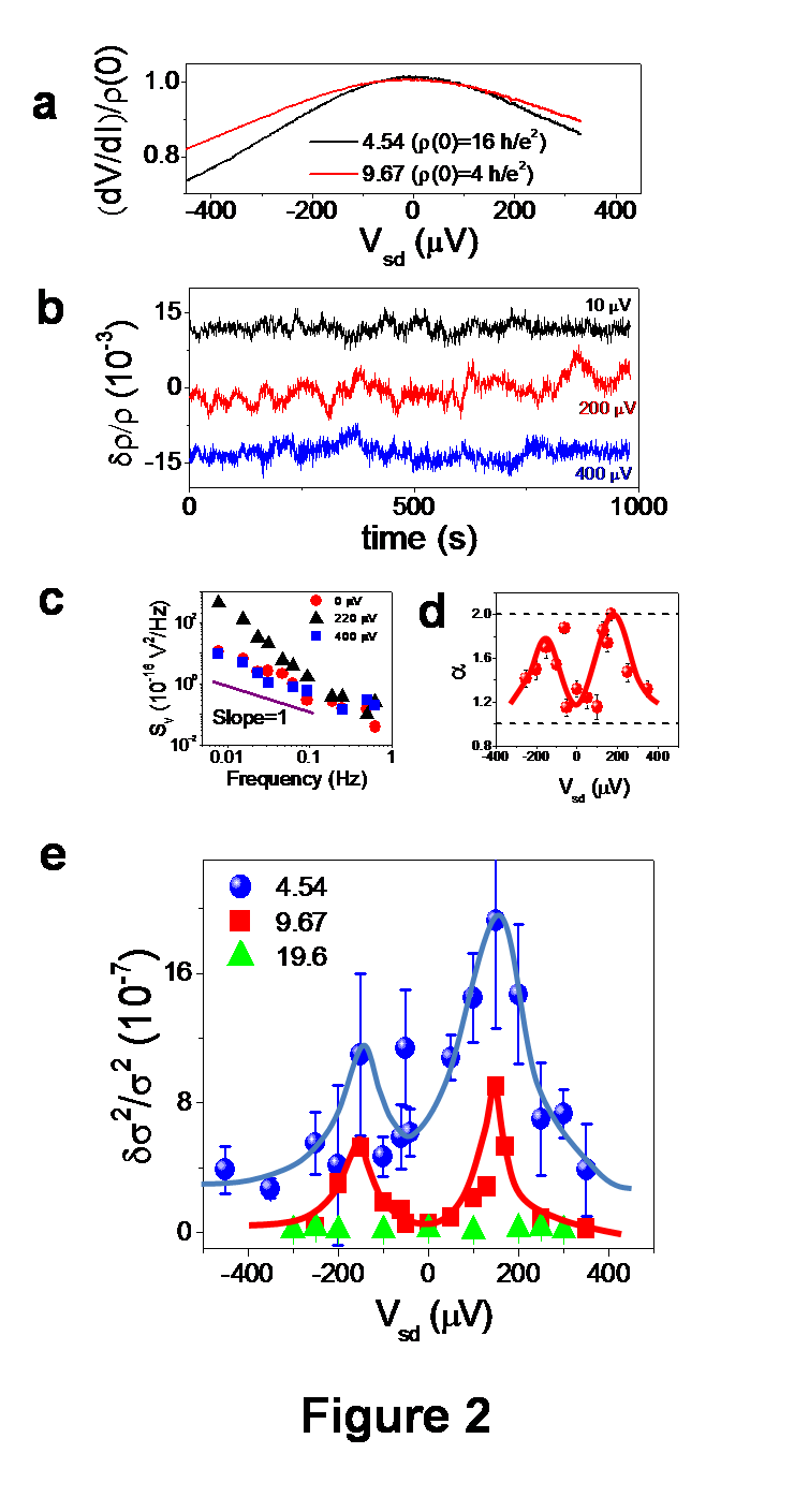
A generic signature of pinned CDW, exploited for 1D Peierls conductors Shobo , as well as magnetically stabilized 2D electron solids Shayegan , is the broad-band noise (BBN) noise from the electric-field induced thermally activated transitions between the metastable steady states. To explore this possibility, we have measured BBN in our mesoscopic devices in a 4-probe differential (ac + dc) mode, where the differential resistance of the mesoscopic region () was measured with a small low-frequency ac modulation (V) added onto a dc source-drain field (). In the insulating regime (resistivity ), decreases, but without any abrupt threshold when increases. This is illustrated for A2678 at mK and T in Fig. 2a. However, when was recorded as a function of time (over several hours) at fixed , we observed a random switching noise for V (see time traces in Fig. 2b). The net variance of noise () hence shows a peak at a device specific of V. Away from this regime, the noise is largely featureless with a power spectral density (Fig. 2c), with the spectral exponent (Fig. 2d), arising from random potential fluctuations at the nearby acceptor sites. As shown in Fig. 2e, the peak in BBN decreases rapidly with increasing , and in the metallic regime, (), it decreases below the measurement background (). The nonmonotonicity in noise is unlikely to arise from hopping, or electron glass behavior Swastik , but can be taken as evidence of electrically driven depinning transition in a pinned CDW Fertig ; Shayegan . The bias at the noise maximum represents the depinning threshold which depends on the quenched disorder, and hence only weakly dependent of . The intermittent plastic flow of the CDW provides the switching noise for which is expected to as indeed observed (Fig. 2d).
Evidence of topological defects was subsequently obtained by focusing on and scrutinizing its dependence on . In accordance with Eq. 1, we find describes the variation of over several decades in all devices over a wide range of (base to 4.5 K) and (see the fits in solid line in Fig. 1b and c where and are constants). This can be readily associated with the proliferation of unbound charged topological defects which dominates electrical conduction in the disordered state (). The self-consistency of the fits was also confirmed by the linearity of in (inset of Fig. 1b), where the -axis intercept gives the magnitude of (within 10% of that obtained from nonlinear fit).
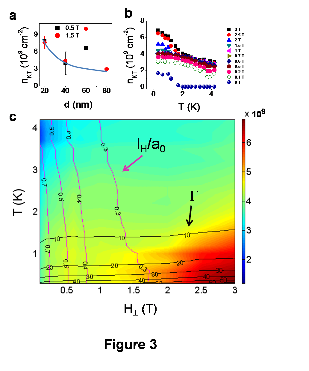
To check if the analysis is physically meaningful, we constructed a melting phase diagram with extracted from the fits. Disorder quenches the kinetic energy of interacting electrons, and stabilizes the ordered state. Hence, decreasing the spacer thickness generally resulted in increasing , unless the background doping dominates the disorder level. As shown in Fig. 3a, decreases from A2407 ( nm) to T546 ( nm), but abruptly large for C2367 ( nm) most likely due to strong background doping (see Methods). In a given device though, disorder is fixed and depends strongly on and , as illustrated for A2678 in Fig. 3b. Note that at T, is nearly cm-2 at low , and corresponds to that is much smaller than the expected for Wigner crystallization in 2DESs without disorder Tanatar .
Fig. 3b illustrates that even a small can increase the melting point dramatically by quenching of quantum fluctuations of the constituent “atomic sites”. It agrees with the recent suggestion that melting of a quantum electron solid needs to be addressed in terms of rather than alone Tsui . (Here and are the magnetic length and mean electron distance, respectively). At higher ( T), a further enhancement in appears at low , pointing towards a different mechanism governing the stability of the CDW. To understand this, we form a surface plot of in space, where the traces of constant classical ( ) and quantum () melting parameters at are shown (Fig. 3c). The top-left corner, where both thermal and quantum fluctuations are strongest, the melting occurs at small , while the bottom-right of the plot represents maximal stability. The abrupt increase in for T occurs when , signifying very little overlap of neighboring wavefunctions and a crossover from quantum to classical electron solid. Melting in this regime is described by , which approaches in the extreme classical limit ( T), agreeing closely with the estimation of by Thouless for a Wigner crystal Thouless .
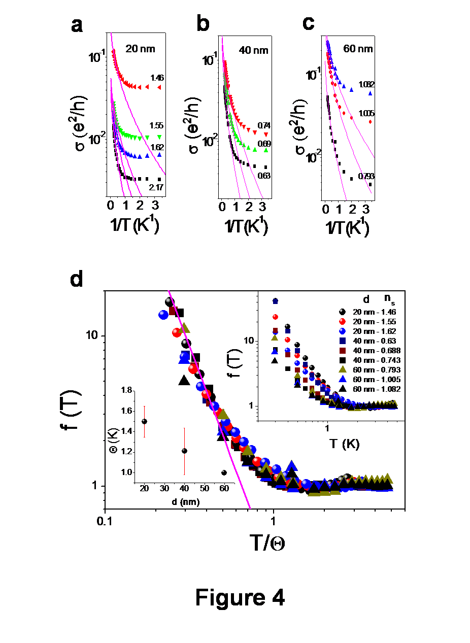
The -dependence of displays a peculiar weakening below a characteristic temperature scale K (Fig. 4a-c) which needs further inspection. This behavior is common to all devices, and the magnitude of was found to be insensitive to changing device length (over a factor of ), eliminating finite size effect as the cause. The dependence of on also indicates to be well-defined, and an explanation based on inhomogeneity-related models does not seem to apply here Tripathi ; Hamilton . To understand this quantitatively, we write . In a “Drude-like” scenario, for instance, , where and would represent the temperature dependence of mean scattering time . The behavior of changes at , which was found to be close to the phonon gap of the electron solid through the following analysis: We obtain the domain size ( nm) from the depinning threshold (V in BBN measurements for A2678 in Fig. 2) Shayegan , from which the phonon gap could be calculated as K (the sound velocity ms-1 is taken to be that of a clean Wigner crystal) Ferconi .
The behavior of can be explained if is determined by an Andreev-Lifshitz (AL)-like mechanism of defect-mediated conduction in a quantum solid AL . For , constant, independent of due to extensive phonon scattering, and the -dependence of is determined by that of only. Hence to extract , we fitted by in the range K (lines in Fig. 4a-c) and subsequently divided it by the fitted trace. The increase in for can be readily understood as freeze out of phonons and delocalization of defects as quantum objects with . A single parameter scaling of the -axis collapses in all devices onto a universal curve, indicating to be the only relevant energy scale (Fig. 4d). We find at (line) with increasing with increasing disorder (i.e. decreasing ) (Fig. 4d(inset)).
Summarizing, there are four key results of this paper: First, both noise measurements and scaling of indicate a quasi ordered ground state in dilute 2DESs at low . The precise nature of ordering is not known, Wigner crystallization being a strong possibility, although it is clear that disorder plays a crucial role in stabilizing such a phase. Second, the BKT scaling provides a new framework within which the transition from strong localization to metallic conduction can be viewed as an order-disorder melting transition. This is in contrast to percolation Sarma , hopping Keuls or Coulomb blockade Ghosh observed in many experiments over the years (mostly in larger or more disordered 2DESs). Third, the BKT transition also implies existence and proliferation of topological defects in 2DES in semiconductors for the first time with tunable number density. Finally, the scaling of the data described in Fig. 4d suggests that a mechanism like AL may apply here and that the topological defects behave as quantum mechanical entities capable of zero point motion and tunneling.
METHODS:
Wafer and device characteristics:
The devices were fabricated from MBE (molecular beam epitaxy) grown GaAs/Al0.33Ga0.66As heterostructures, where the two-dimensional electron gas was formed nm below the surface. In all devices, delta (monolayer)-doping of Si ( cm-2) was implemented. The strength of the disorder is partially determined by the thickness of the spacer layer (undoped Al0.33Ga0.66As) situated between the heterostructure interface and dopant layer. The typical as-grown electron mobility was found between cm2/V.s at cm-2. The wafers T546 ( nm) and C2367 ( nm) were grown in different chambers to observe the influence of background doping. The details of various devices used in our experiment are shown in Table 1:
| Wafer | ||||
|---|---|---|---|---|
| A2407 | 2.5 | 20 | 0.5 | |
| A2678 | 2.5 | 40 | 0.5 | |
| C2367 | 0.7 | 60 | 1.0 | |
| T546 | 1.9 | 80 | 0.9 | 0.3 |
Table 1. Details of devices used in our measurements showing the doping concentration ( cm-2), spacer thickness (nm), as-grown mobility ( cm2/V.s) and background doping estimate ( cm-3).
Measurements:
The noise measurements were carried out inside a He-3 cryostat (base electron temperature 270 mK), using a four-probe ac+dc technique with the ac bias fixed at V at an excitation frequency of 128 Hz, and dc bias varied over V. The voltage fluctuations across the sample were measured using a lock-in amplifier whose output was subsequently digitized using a 16-bit digitizer, followed by decimation and power spectral density (PSD) calculations using Welch’s method of averaged periodogram.
References
- (1) Laughlin, R.B. Anamalous Quantum Hall Effect: An incompressible quantum fluid with fractionally charged excitations. Phys. Rev. Lett. 50, 1395-1398 (1983).
- (2) Nayak, C. et al. Non-Abelian anyons and topological quantum computation. Rev. Mod. Phys. 80, 1083-1159 (2008).
- (3) Berezenskii, V.L. Destruction of long-range order in one-dimensional and two-dimensional systems possessing a continuous symmetry group. \@slowromancapii@. Quantum systems. Sov. Phys. JETP 34, 610-616 (1972).
- (4) Kosterlitz, J.M. & Thouless, D.J. Ordering, metastability and phase-transitions in 2 dimensional systems. J. Phys. C 6, 1181-1203 (1973).
- (5) Das Sarma, S. et al. Two-Dimensional Metal-Insulator Transition as a Percolation Transition in a High-Mobility Electron System. Phys. Rev. Lett. 94, 136401 (2005).
- (6) Tanatar, B. & Ceperley, D.M. Ground state of the two-dimensional electron gas. Phys. Rev. B 39, 5005-5016 (1989).
- (7) Chen, Y.P.et al. Melting of a 2D quantum electron solid in high magnetic field. Nat. Phys. 2, 452-455 (2006).
- (8) Ye, P.D. et al. Correlation lengths of the wigner-crystal order in a two-dimensional electron system at high magnetic fields. Phys. Rev. Lett. 89, 176802 (2002).
- (9) Camjayi, A., Haule, K., Dobrosavljevic, V. & Kotliar, G. Coulomb correlations and the Wigner-Mott transition. Nat. Phys. 4, 932-935 (2008).
- (10) Eguiluz, A.G. & Maradudin, A.A. Two-dimensional Wigner lattice in a msgnetic field and in the presence of a random array of pinning centers. Phys. Rev. B 27, 4933-4945 (1983).
- (11) Sambandamurthy, G. et al. Observation of pinning mode of stripe phases of 2D systems in high Landau levels. Phys. Rev. Lett. 100, 256801 (2008).
- (12) Koulakov, A.A., Fogler, M.M. & Shklovskii, B.I. Charge density wave in two-dimensional electron liquid in weak magnetic field. Phys. Rev. Lett. 76, 499-502 (1996).
- (13) Spivak, B. & Kivelson, S.A. Phases intermediate between a two-dimensional electron liquid and Wigner crystal. Phys. Rev. B 70, 155114 (2004).
- (14) Thouless, D.J. Melting of the two-dimensional Wigner lattice. J. Phys. C 11, L189-L190 (1978).
- (15) Min-Chul Cha & Fertig, H.A. Topological defects, orientational order, and depinning of the electron solid in a random potential. Phys. Rev. B 50, 14368-14380 (1994).
- (16) Halperin, B. I. & Nelson, D. R., Theory of two dimensional melting. Phys. Rev. Lett. 41, 121 (1978); E41, 519 (1978).
- (17) Young, A. P. Melting and the vector Coulomb gas in two dimensions. Phys. Rev. B 19, 1855 (1979).
- (18) Checkelsky, J.G., Lu Li & Ong, N.P. Zero-energy state in graphene in a high magnetic field. Phys. Rev. Lett. 100, 206801 (2008).
- (19) Tripathi, V. & Kennett, M.P. Magnetotransport in disordered delta-doped heterostructures. Phys. Rev. B 74, 195334 (2006).
- (20) Neilson, D. & Hamilton, A. Tunneling and hopping between domains in the metal-insulator transition in two-dimensions. Int. Jour. Mod. Phys. B 22, 4565-4571 (2008).
- (21) Baenninger, M. et al. Local transport in a disordered-stabilized correlated insulating phase. Phys. Rev. B 72, 241311 R (2005).
- (22) Baenninger, M. et al. Low-temperature collapse of electron localization in two dimensions. Phys. Rev. Lett. 100, 016805 (2008).
- (23) Bhattacharya, S. et al. Origin of broadband noise in charge-density-wave conductors. Phys. Rev. Lett. 54, 2453-2456 (1985).
- (24) Yuan, P. Li. et al. Low-frequency noise in the reentrant insulating phase around the 1/5 fractional quantum hall liquid. Phys. Rev. Lett. 67, 1630-1633 (1991).
- (25) Kar, S. et al. Observation of non-gaussian conductance fluctuations at low temperatures in Si:P(B) at the metal-insulator transition. Phys. Rev. Lett. 91, 216603 (2003).
- (26) Ferconi, M. & Vignale, G. Theory of the pinning gap in the phonon spectrum of a disordered Wigner crystal. Phys. Rev. B 48, 2831-2834 (1993).
- (27) Andreev, A.F. & Lifshitz, I.M. Quantum theory of defects in crystals. Sov. Phys. JETP. 29, 1107-1113 (1969).
- (28) Van Keuls, F.W. et al. Localization scaling reltion in two dimensions: Comparison with experiment. Phys. Rev. B 56, 13263-13267 (1997).
- (29) Ghosh, A. et al. Density-dependent instabilities in correlated two dimensional electron systems. J. Phys. Condens. Matter 16, 3623-3631 (2004).