Andreev reflection enhanced single hole tunneling in Ge/Si core/shell nanowire quantum dot
Abstract
We experimentally study the electrical transport properties of Ge/Si core/shell nanowire device with two superconducting leads in the Coulomb blockade regime. Anomalous zero field magneto-conductance peaks are observed for the first time at the gate voltages where Coulomb blockade oscillation peaks present. Many evidences indicate this feature is due to Andreev reflection enhanced phase coherent single hole tunneling through the quantum dot, which can be suppressed by an external magnetic field without destroying the superconducting states in the electrodes.
The novel and fruitful electrical transport phenomena when carbon nanotubes Kasumov et al. (1999); Morpurgo et al. (1999); Buitelaar et al. (2002); Jarillo-Herrero et al. (2006); Jørgensen et al. (2006); Cleuziou et al. (2007), semiconductor nanowires Doh et al. (2005); van Dam et al. (2006); Xiang et al. (2006); Sand-Jespersen et al. (2007); Doh et al. (2008); Li et al. (2010) or graphene Heersche et al. (2007); Miao et al. (2007); Shailos et al. (2007); Du et al. (2008); Ojeda-Aristizabal et al. (2009); Kessler et al. (2010) are connected to superconductor have attracted special attention in recent years. In these nano-scale devices, transport properties will highly depend on the transparency of the interface between the superconducting electrodes and the nano-structure embedded between them. For fully transparent contacts, proximity effect will induce supercurrent and multiple Andreev reflections in the device Kasumov et al. (1999); Doh et al. (2005); van Dam et al. (2006); Xiang et al. (2006); Heersche et al. (2007); Miao et al. (2007); Du et al. (2008); Ojeda-Aristizabal et al. (2009); Shailos et al. (2007); Cleuziou et al. (2007). For intermediately transparent contacts, interaction between Andreev reflection and Fabry-Perot interference Jarillo-Herrero et al. (2006); Jørgensen et al. (2006) or Kondo resonance Buitelaar et al. (2002); Sand-Jespersen et al. (2007) can be observed. For lowest transparent contacts, the non-superconductor between two electrodes forms a quantum dot, and only superconducting gap opened in Coulomb blockade regime presents Doh et al. (2008); Li et al. (2010). Interestingly, we find that our experimental system just falls into the region between the last two situations mentioned above, which shows Andreev reflection enhanced single hole tunneling (SHT) through the quantum dot at the center of Coulomb blockade oscillation peaks, instead of SHT blocked by superconducting gap in electrodes. Moreover, in the previous investigations of similar structures, magneto-conductance through the sample was typically not studied. Here, we measured the magneto-conductance and observed that the phase information during the Andreev reflection enhanced SHT process can be destroyed by an external magnetic field before the superconducting states quenching in the electrodes. Such a SHT tunneling mechanism has not been observed and reported previously.
The devices reported were fabricated on undoped Ge/Si core/shell nanowires grown by two-step chemical vapor deposition Lu et al. (2005). Due to the large valence band offset between the Ge core and the Si shell, one-dimensional hole gas can be confined in the Ge channel. Then we wet transferred nanowires to heavily doped Si wafer with silicon oxide, which was used as a back gate in the measurement. After locating the nanowires relative to the predefined markers on substrate using Scanning Electron Microscope (SEM), source and drain contacts were designed by electron-beam lithography. To remove the native oxide outside the Si shell of the nanowires for good contact, we immersed the sample in buffered hydrofluoric acid for seconds. Then thickness of superconducting Aluminum (Al) were deposited. Fortunately, without annealing, we still obtained nearly ideal Ohmic contacts between the Al leads and the nanowires Li et al. (2010). SEM image of one of our samples is shown in the inset of Fig. 1(a).
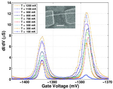
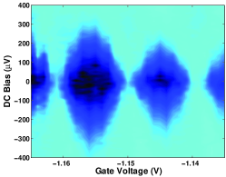
The measurements were performed in a top-loading dilution refrigerator with an environment base temperature of . In the measurements, We employed the standard AC lock–in technique with an excitation voltage of at . Similar behaviors were observed in several devices, and here we show data obtained from two of them (Fig. 1 and Fig. 5 are taken from one sample, and the others are from the other one). Using the back gate to tune the energy levels in the quantum dot, we saw clear Coulomb blockade peaks at a wide range of . From the Coulomb blockade oscillations, we obtained an average gate voltage separation of , as shown in Fig. 1(a). Using the cylinder-on-plane model Lu et al. (2005), we calculated the effective length of the quantum dot to be around , which is consistent with the sample size. After considering the pinch off gate voltage of around , we estimated holes are typically left in the dot.
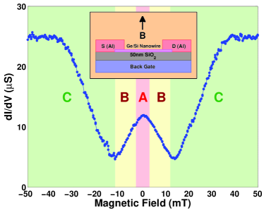
We then measured the magneto-conductance by fixing at one of the Coulomb blockade oscillation peaks and applying a magnetic field perpendicular to both the axis of the nanowire and the substrate. For very low interface transparency sample, SHT will be blocked when the energy difference between the source and the drain is less than the quasi-particle superconducting gap in the Al-leads Krstić et al. (2003). So in the stability diagram, in which differential conductance is plotted as a function of source drain bias and gate voltage , a gap of ( is the element charge) will be opened at the cross point of two adjacent Coulomb diamonds Doh et al. (2008). Meanwhile, a zero conductance dip with width of at magnetic field Li et al. (2010) will be observed in the magneto-conductance data. Here is the maximal magnetic field to preserve Al electrodes in superconducting states, which is so called critical magnetic field. This kind of dip can still be seen in our data as shown in Fig. 1(b). But different from previous experiments, we find a remarkable peak at the center of the expected differential conductance dip region. From the conductance values at Coulomb blockade peaks in normal state ( parts in Fig. 1(b)), we estimated the tunneling rate between the source/drain lead and the quantum dot is around . This value is still smaller than the superconducting gap , but much larger than the values, which are around , we obtained from the low transparency samples Li et al. (2010).
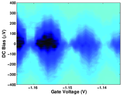
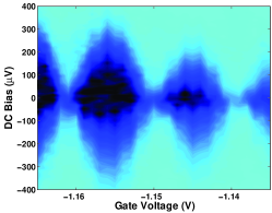
In order to illustrate the evolution of the stability diagram during the magnetic field increasing, we plotted three stability diagrams in Fig. 2, at different magnetic fields (Fig. 2(a)), (Fig. 2(b)), and (Fig. 2(c)). The light blue (dark black) parts in these figures represent large (small) values of differential conductance . It is obvious that the gap at , which should be widest at according to previous reports Doh et al. (2008); Li et al. (2010), is indeed a little bit closed at in our system. The gap starts to open as the magnetic field growing up, and reaches a maximum at but is still significantly less than . After , this gap gradually vanishes along with the Al leads turning into normal (non-superconducting) states.
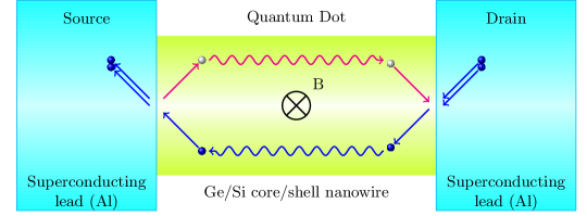
The abnormal magneto-conductance presented here is apparently different from the ones reported before Li et al. (2010), which implies that a new transport mechanism exists in this system. First of all, we did not observe any evidence of Kondo effect in any of our devices having these magneto-conductance features. In addition, the Kondo resonance induced effect occurs in the dips of Coulomb blockade oscillations Buitelaar et al. (2002), while the anomalous peak here were observed at the peaks of Coulomb blockade oscillations. These arguments exclude the influence of Kondo resonances to the SHT process. Since the magneto-transport shows negative magneto-conductance at very low field, weak antilocalization could be one possible origination of the zero field peak. However, based on our previous investigation of weak antilocalization and spin-orbit coupling on this system Hao et al. (2010), the drop of conductance could not be so strong for a change of several milliteslas in magnetic field. Besides, the high temperature ( larger than the critical temperature of Al: ) data does not show this kind of peak, but the weak antilocalization survives even as the temperature goes beyond . Here, we explain our data as Andreev reflection enhanced SHT through the quantum dot. In the Andreev reflection, when an electron (hole) from non-superconducting material incidents at the interface of superconductor and non-superconductor, it will be reflected with the opposite spin and momentum as a phase-conjugated hole (electron), and forms a Cooper pair in the superconductor Andreev (1964). In our system, as shown in Fig. 3, one hole runs in the nanowire and incident at the interface of the nanowire and the drain, it will be reflected as an electron in the nanowire and also destroys a Cooper pair in the drain. Then the electron travels through the nanowire and incidents at another interface, the one between the nanowire and the source, it will be reflected as a hole and create a Cooper pair in the source. This theory well explains the features observed in Fig. 1(b). There are three regions labeled as ‘A’, ‘B’ and ‘C’. In the region ‘A’, even if there are superconducting gaps in the source and drain leads, current can still flow through the device continuously at zero bias. In this way, the SHT process is actually enhanced by Andreev reflections. In addition, because of the Andreev reflections can preserve the phase information, the Andreev reflection enhanced SHT transport is phase coherent Doh et al. (2005). While in region ‘B’, an external magnetic field less than applied perpendicular to the transport channel will break the phase information during the transport. That is why the phase coherent transport is suppressed and the differential conductance decreases while the magnetic field increases. In region ‘C’, larger magnetic field exceeding the critical field destroys the superconducting states in electrodes. So the transport will come back to the normal Coulomb blockade oscillation regime and the conductance will recover to the normal value.
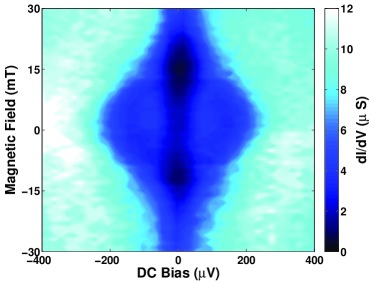
The Andreev reflection enhanced SHT explanation was supported by additional data. In Fig. 4(a), the differential conductance is plotted against the magnetic field and the DC bias voltage while fixing at the Coulomb blockade oscillation peak. In this figure, it is clearly seen that at , has a local maximum at zero field and decreases as increasing, then goes up and stabilizes after . The magneto-conductance feature is observed not only at but also at all voltages because of inelastic tunneling. The temperature dependence of the Coulomb blockade oscillations shown in Fig. 1(a) implies the energy level splitting in the quantum dot is much smaller than , where is Boltzmann’s constant and is the temperature of charge carriers. It means the dot we measured was in classical Coulomb blockade regime, where inelastic tunneling can easily happen. This is consistent with the quantum dot being in the many–hole regime, confirmed by the holes left in the dot discussed before. In addition, as shown in the light blue regions in Fig. 2, differential conductance keeps increasing also indicates inelastic tunneling through the quantum dot. Therefore, in our quantum dot, as a result of excited states falling into the gap broadened by temperature and inelastic tunneling, Andreev reflection enhanced SHT can still happen even if the ground state energy level in the quantum dot is not exactly aligned with the Fermi levels of the source or drain.
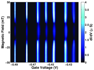
Gate voltage dependence of magneto-conductance is displayed in the color-scale plot of Fig. 4(b), in which we find the interesting magneto-conductance peak feature appears at each Coulomb oscillations peak. But the strength of the peak depends on the Coulomb oscillation in the normal state. This is consistent with that the probability of Andreev reflection occurs depends on the effective transparency of the interface, i.e. the alignment of energy levels in the quantum dot with Fermi levels in the source and drain electrodes Buitelaar et al. (2003); Jarillo-Herrero et al. (2006). By means of a gate voltage, the Andreev enhanced SHT are modulated as well as the Coulomb oscillations. This gate tunable phenomenon is similar as reported by Jarillo-Herrero et al. Jarillo-Herrero et al. (2006). In their experiments, the supercurrent and multiple Andreev reflections can be turned on and off by gating the carbon nanotube at different Febry-Perot interference regions. Notably, the normal state conductance in the region where supercurrent observed in their device is slightly higher than ours but in the same order of ( is the Planck’s constant). The key factor which is responsible for the Andreev reflection enhanced phase coherent SHT in our system is the interface transparency. The interface in our case is a little opaque but not opaque enough to prevent the Andreev reflection process. Therefore, in our case the transport is dominated by SHT events and the gate voltage tunes the position of the energy levels and opens a channel at the position where SHT is enhanced through multiple Andreev reflections.
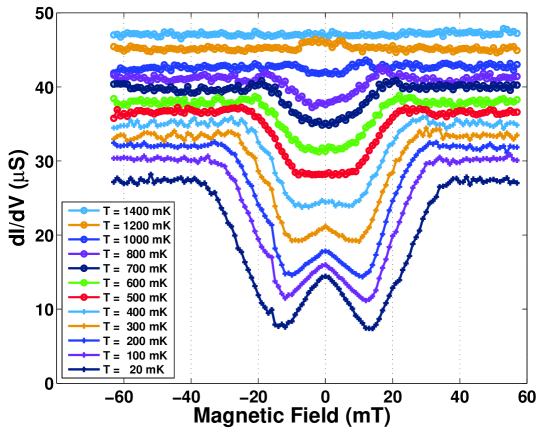
We also tested the device at different temperatures. From the data given in Fig. 5, we find that the conductance dip owing to SHT blocked by superconducting gap collapses and finally disappears at Li et al. (2010). But the Andreev reflection enhanced SHT feature vanishes before Al leads lose superconductivity at around , at which temperature the superconducting gap in Al starts to decrease dramatically according to the superconductivity theory Li et al. (2010), and does not show up after . These experimental phenomena are consistent with the explanation in Fig. 3, and suggest that the phase coherent transport is directly correlated to the superconducting states in the electrodes and is much easier to be destroyed by heating effect than the superconducting state in Al.
In conclusion, we observed magneto-conductance peak at zero magnetic field on superconductor contacted Ge/Si core/shell nanowire quantum dot at the point of Coulomb blockade oscillation peak. The experimental data are consistent with our explanation — Andreev reflection enhanced phase coherent single hole tunneling through the quantum dot. Neither the demonstrated results nor suggested transport mechanism has been reported before in previous literature, and both of them justify further exploring experimentally and theoretically.
This work was supported by the National Basic Research Program of China (Grants No. 2009CB929600, No. 2006CB921900), the National Natural Science Foundation of China (Grants No. 10804104, No. 10874163, No. 10604052, 10934006), and the US National Science Foundation (ECS-0601478).
References
- Kasumov et al. (1999) A. Y. Kasumov, R. Deblock, M. Kociak, B. Reulet, H. Bouchiat, I. I. Khodos, Y. B. Gorbatov, V. T. Volkov, C. Journet, and M. Burghard, Science 284, 1508 (1999).
- Morpurgo et al. (1999) A. F. Morpurgo, J. Kong, C. M. Marcus, and H. Dai, Science 286, 263 (1999).
- Buitelaar et al. (2002) M. R. Buitelaar, T. Nussbaumer, and C. Schönenberger, Phys. Rev. Lett. 89, 256801 (2002).
- Jarillo-Herrero et al. (2006) P. Jarillo-Herrero, J. A. van Dam, and L. P. Kouwenhoven, Nature 439, 953 (2006).
- Jørgensen et al. (2006) H. I. Jørgensen, K. Grove-Rasmussen, T. Novotný, K. Flensberg, and P. E. Lindelof, Phys. Rev. Lett. 96, 207003 (2006).
- Cleuziou et al. (2007) J.-P. Cleuziou, W. Wernsdorfer, S. Andergassen, S. Florens, V. Bouchiat, T. Ondarçuhu, and M. Monthioux, Phys. Rev. Lett. 99, 117001 (2007).
- Doh et al. (2005) Y.-J. Doh, J. A. van Dam, A. L. Roest, E. P. A. M. Bakkers, L. P. Kouwenhoven, and S. De Franceschi, Science 309, 272 (2005).
- van Dam et al. (2006) J. A. van Dam, Y. V. Nazarov, E. P. A. M. Bakkers, S. De Franceschi, and L. P. Kouwenhoven, Nature 442, 667 (2006).
- Xiang et al. (2006) J. Xiang, A. Vidan, M. Tinkham, R. M. Westervelt, and C. M. Lieber, Nature Nanotech. 1, 208 (2006).
- Sand-Jespersen et al. (2007) T. Sand-Jespersen, J. Paaske, B. M. Andersen, K. Grove-Rasmussen, H. I. Jørgensen, M. Aagesen, C. B. Sørensen, P. E. Lindelof, K. Flensberg, and J. Nygård, Phys. Rev. Lett. 99, 126603 (2007).
- Doh et al. (2008) Y.-J. Doh, S. D. Franceschi, E. P. A. M. Bakkers, and L. P. Kouwenhoven, Nano Lett. 8, 4098 (2008).
- Li et al. (2010) H.-O. Li, X.-J. Hao, C. Zhou, G. Cao, T. Tu, G.-C. Guo, G.-P. Guo, W. Y. Fung, Z. Ji, and W. Lu (2010), in preparation.
- Heersche et al. (2007) H. B. Heersche, P. Jarillo-Herrero, J. B. Oostinga, L. M. K. Vandersypen, and A. F. Morpurgo, Nature 446, 56 (2007).
- Miao et al. (2007) F. Miao, S. Wijeratne, Y. Zhang, U. C. Coskun, W. Bao, and C. N. Lau, Science 317, 1530 (2007).
- Shailos et al. (2007) A. Shailos, W. Nativel, A. Kasumov, C. Collet, M. Ferrier, S. Guéron, R. Deblock, and H. Bouchiat, Europhys. Lett. 79, 57008 (2007).
- Du et al. (2008) X. Du, I. Skachko, and E. Y. Andrei, Phys. Rev. B 77, 184507 (2008).
- Ojeda-Aristizabal et al. (2009) C. Ojeda-Aristizabal, M. Ferrier, S. Guéron, and H. Bouchiat, Phys. Rev. B 79, 165436 (2009).
- Kessler et al. (2010) B. M. Kessler, Ç. Ö. Girit, A. Zettl, and V. Bouchiat, Phys. Rev. Lett. 104, 047001 (2010).
- Lu et al. (2005) W. Lu, J. Xiang, B. P. Timko, Y. Wu, and C. M. Lieber, Proc. Natl. Acad. Sci. U. S. A. 102, 10046 (2005).
- Krstić et al. (2003) V. Krstić, S. Roth, M. Burghard, J. Weis, and K. Kern, Phys. Rev. B 68, 205402 (2003).
- Hao et al. (2010) X.-J. Hao, T. Tu, H.-O. Li, C. Zhou, G. Cao, G.-C. Guo, W. Y. Fung, Z. Ji, G.-P. Guo, and W. Lu (2010), submitted.
- Andreev (1964) A. F. Andreev, Sov. Phys. JETP 19, 1228 (1964).
- Buitelaar et al. (2003) M. R. Buitelaar, W. Belzig, T. Nussbaumer, B. Babić, C. Bruder, and C. Schönenberger, Phys. Rev. Lett. 91, 057005 (2003).