Compact silicon double and triple dots realized with only two gates.
Abstract
We report electronic transport on silicon double and triple dots created with the optimized number of two gates. Using silicon nitride spacers two dots in series are created below two top gates overlapping a silicon nanowire. Coupling between dots is controlled by gate voltages. A third dot is created either by combined action of gate voltages or local doping depending on the spacers length. The main characteristics of the triple dot stability diagram are quantitatively fitted.
Semiconducting quantum dots are usually made with three gates: one plunger gate to control the density of carriers and two gates to control the in and out tunneling rates. A recent achievement is a controlled silicon Single Electron Transistor (SET) using only one gate. This MOS-SET departs from the usual MOSFET Hofheinz06B ; Hofheinz06 by a specific design of channel junctions to source and drain. Tunnel barriers are formed by undoped silicon segments and a quantum dot is created by accumulation of carriers below the gate. The undoped silicon barriers sit below spacers which are used as a mask during source and drain implantation.
In this work we show that the association of two MOS-SETs in series — the most natural extension of the single MOS-SET — yields both a well controlled double dot with tunable inter-coupling and a triple dot. Within other technologies triple dots usually require many gates. Triple dots have been realized in 2DEG Waugh95 ; Schroer07 ; Vidan04 and in silicon using top and side gates Lee00 . The advantage of a single gate design becomes crucial when compact arrangements of multiple quantum dots are required, for instance to create high fidelity electron pumps, latching switches, quantum cellular automata Orlov01 , single-electron-parametron devices Korotkov98 , non-local interacting qubits Hollenberg06 ; Greentree04 or rectifier devices Stopa02 ; Vidan04 ; Ferrari05 .
Recently silicon quantum dot molecules, i.e. a double dot with tunable coupling, have been built with one larger upper gate plus four side gates Shin07 or three top gates Liu08 . Reducing further the number of gates has been possible at the cost of stochasticity: a coupled quantum dot was obtained with two top and one upper gates by relying on the static disordered potential arising from the Si/SiO2 buried oxide interface rugosity Liu08B . One advantage of our technology is that our double and triple dots are smaller and/or simpler than previously reported Waugh95 ; Schroer07 ; Vidan04 ; Lee00 ; Shin07 ; Liu08 .
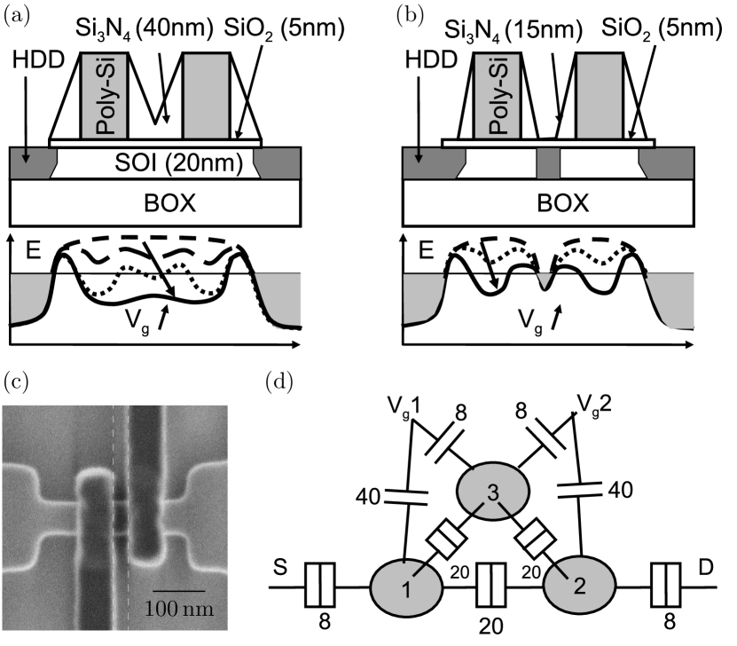
Our samples are produced on 200 mm silicon-on-insulator (SOI) wafers in a CMOS platform. A 200 nm long, 20 nm thick and –60 nm wide silicon nanowire is etched and covered by two –60 nm long polysilicon gates isolated by 5 nm thick SiO2 gate oxide (Fig. 1). The spacing between gates is –60 nm. 15 or 40 nm thick silicon nitride spacers are deposited on both sides of the gates. Therefore for samples with long (40 nm) spacers (samples 1 and 2) the silicon region between the gates is undoped as it is masked during the heavy As implantation of the source and drain. On the contrary it is doped for samples with short (15 nm) spacers (sample 3). Samples with thinner SOI (10 nm) have also been studied and the increase of the period of Coulomb blockade oscillations (CBO) shows that the size of each MOS-SET is further reduced (not shown). The typical charging energy of our MOS-SETs is 2 meV.
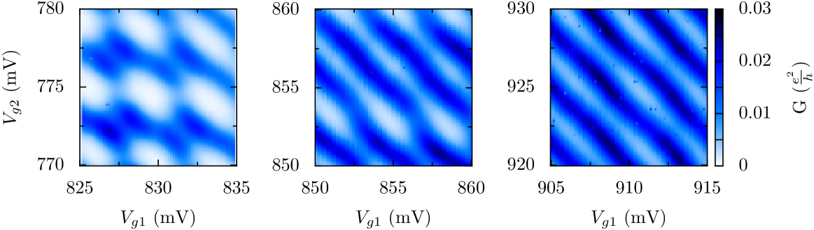
Figure 2 shows the drain-source current versus gate voltages applied on each gate at K in a device with 40 nm long spacers. Two nominally identical MOS-SETs appear below the two gates, with CBO periods very constant in gate voltage Hofheinz06B . Similar CBO periods and threshold voltages are observed for the two MOS-SETs, illustrating the reproductibility of the fabrication process. At low () the two dots are decoupled and the 2D plot exhibits the expected square lattice pattern Vanderwiel03 (not shown). At intermediate () the dots are capacitively coupled and the 2D plot shows the so-called honeycomb pattern (Fig. 2, left panel). The gate capacitances , and the interdot capacitance are estimated to 40 aF, 40 aF and 20 aF respectively. At large () the tunnel coupling becomes non negligible and the 2D plot exhibits characteristic wandering anti-diagonals Vanderwiel03 ; Liu08 (Fig. 2, central panel). At even larger gate voltages the two dots merge into a single island (Fig. 2 right panel). In that case the period along the diagonal in () plot is half that of the two separated dots, as expected since the gate capacitance is approximately twice larger for the single merged dot. This evolution, similar to the ones reported in Ref. Liu08, ; Liu08B, , shows that a tunable double dot is obtained with only two gates. The absence of independent control on the carrier’s number and interdot coupling is compensated by the compacity and simplicity of our devices.
The transition from two independent dots towards a single island is realized by increasing simultaneously the two gate voltages which both control the potential of the undoped silicon nanowire segment separating the two MOS-SETs. This evolution is not monotonic. A periodic antidiagonal (i.e. constant value) pattern is superimposed (see Fig. 3). This period results from Coulomb blockade on a third intermediate dot created in the silicon nanowire, at equal distance from both gates. It arises from the combined action of the two unscreened gate potentials in samples with long spacers (see Fig. 1a). The whole system then behaves as three dots in series controlled by two gate voltages. In order to model this triple dot we consider the electrostatic configuration depicted in Fig. 1d. The conductance is simulated within the orthodox model of Coulomb blockade without cotunneling Hofheinz06 ; Pierre09 . Cotunneling through dot 3 is nevertheless taken into account as a direct tunnel coupling between dots 1 and 2. For the sake of simplicity the five tunnel junctions tunneling rates are taken equal. The capacitance values indicated in Fig. 1d give the best fit for the periods measured in sample 2. These values also describe well sample 1. We note that these tunnel capacitances are larger than their simple planar geometrical approximations ( aF instead of 3 aF for instance). This effect is attributed to the large polarizability of electrons in the tunnel barriers with small energy height Hofheinz07 .
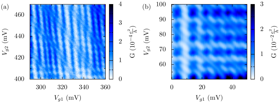
The tunnel coupling between the two MOS-SETs as well as the occurence of the third dot can also be tuned by doping. Indeed in samples with small spacers (sample 3) the central region of the SOI nanowire is not protected and is therefore n-doped (see Fig. 1b). Thus at zero gate voltages the central region contains electrons. This doped architecture is reminiscent of the locally implanted silicon quantum dots Jamieson05 . The voltage at which source-drain current is detected at low temperature is in short spacers samples, whereas it is detected at larger values ( V) in long spacers samples. The honeycomb pattern for both kind of samples exhibit similar periods, showing that the characteristics of each MOS-SET is not affected by the central doping. On the contrary the central dot is strongly modified: the period of the anti-diagonals is reduced by a factor 2.5, which indicates a bigger central dot more capacitively coupled to gates (see Fig. 3b).
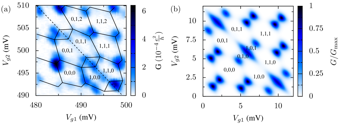
On Fig. 4a a detail of the diagram is shown at lower temperature ( K) in sample 2 for one of these anti-diagonals. The corresponding simulation shown in Fig. 4b reproduces the distorted honeycomb pattern experimentally observed, except for lines joining the triple points which are a consequence of cotunneling. The number of electrons () on each dot is indicated in Fig. 4b. , , are determined by dividing counted from the threshold ( V) by the CBO period and the figure is periodic in ,, (see Fig. 3). Far from the degeneracy () of dot 3 one recovers the honeycomb pattern for the double dot system. Near degeneracy we observe an alternance of pentagones and diamonds. Up to eight triple points per cell are predicted for a triple dot Schroer07 . In case of high symmetry and perfect matching between the capacitances these eight points can reduce to four quadruple points Schroer07 , as observed in both our simulation and data (see Fig. 4).
In conclusion we have shown that the MOS-SET device Hofheinz06B can be extended to multiple dots with a minimal number of gates. A triple dot has been realized for the first time in silicon with only two control gates. It consists of two MOS-SETs in series separated by a locally n-doped or undoped silicon nanowire. The obtained triple dot is very compact and can be used to design more complex circuits based on single electron transfers.
The research leading to these results has received funding from the European Community’s seventh Framework (FP7 2007/2013) under the Grant Agreement Nr:214989. The samples subject of this work have been designed and made by the AFSID Project Partners http://www.afsid.eu. E.P., M.B. and M.F. would like to acknowledge S. Cocco (Laboratorio Nazionale MDM) who contributed to develop the the transport acquisition equipment.
References
- (1) M. Hofheinz, X. Jehl, M. Sanquer, G. Molas, M. Vinet and S. Deleonibus, Appl. Phys. Lett. 89, 143504 (2006).
- (2) M. Hofheinz, X. Jehl, M. Sanquer, G. Molas, M. Vinet and S. Deleonibus, Eur. Phys. J. B 54, 299 (2006).
- (3) F. R. Waugh, M. J. Berry, D. J. Mar, R. M. Westervelt, K. L. Campman and A. C. Gossard, Phys. Rev. Lett. 75, 705 (1995).
- (4) D. Schröer, A. D. Greentree, L. Gaudreau, K. Eberl, L. C. L. Hollenberg, J. P. Kotthaus and S. Ludwig, Phys. Rev. B 76, 075306 (2007).
- (5) A. Vidan, R. M. Westervelt, M. Stopa, M. Hanson and A. C. Gossard, Appl. Phys. Lett. 85, 3602 (2004).
- (6) S. D. Lee, K. S. Park, J. W. Park, J. B. Choi, S.-R. E. Yang, K.-H. Yoo, J. Kim, S. I. Park and K. T. Kim, Phys. Rev. B 62, R7735 (2000).
- (7) A. O. Orlov, R. K. Kummamuru, R. Ramasubramaniam, G. Toth, C. S. Lent, G. H. Bernstein and G. L. Snider, Appl. Phys. Lett. 78, 1625 (2001).
- (8) A. N. Korotkov and K. K. Likharev, J. of Appl. Phys. 84, 6114 (1998).
- (9) L. C. L. Hollenberg, A. D. Greentree, A. G. Fowler and C. J. Wellard, Phys. Rev. B 74, 045311 (2006).
- (10) A. D. Greentree, J. H. Cole, A. R. Hamilton and L. C. L. Hollenberg, Phys. Rev. B 70, 235317 (2004).
- (11) M. Stopa, Phys. Rev. Lett. 88, 146802 (2002).
- (12) G. Ferrari, L. Fumagalli, M. Sampietro, E. Prati, M. Fanciulli, J. of Appl. Phys. 98, 044505 (2005).
- (13) S. J. Shin, J. J. Lee, R. S. Chung, M. S. Kim, E. S. Park, J. B. Choi, N. S. Kim, K. H. Park, S. D. Lee, N. Kim and J. H. Kim, Appl. Phys. Lett. 91, 053114 (2007).
- (14) H. Liu, T. Fujisawa, H. Inokawa, Y. Ono, A. Fujiwara and Y. Hirayama, Appl. Phys. Lett. 92, 222104 (2008).
- (15) H. W. Liu, T. Fujisawa, Y. Ono, H. Inokawa, A. Fujiwara, K. Takashina and Y. Hirayama, Phys. Rev. B 77, 073310 (2008).
- (16) W. G. Van der Wiel, S. De Franceschi, J. M. Elzerman, T. Fujisawa, S. Tarucha and L. P. Kouwenhoven, Review Modern Phys. 75, 1 (2003).
- (17) M. Pierre, M. Hofheinz, X. Jehl, M. Sanquer, G. Molas, M. Vinet and S. Deleonibus, Eur. Phys. J. 70, 475 (2009).
- (18) M. Hofheinz, X. Jehl, M. Sanquer, G. Molas, M. Vinet and S. Deleonibus, Phys. Rev. B 75, 235301 (2007).
- (19) D. N. Jamieson, C. Yang, T. Hopf, S. M. Hearne, C. I. Pakes, S. Prawer, M. Mitic, E. Gauja, S. E. Andresen, F. E. Hudson, A. S. Dzurak and R. G. Clark, Appl. Phys. Lett. 86, 202101 (2005).