From stochastic single atomic switch to nanoscale resistive memory device
We study the switching characteristics of nanoscale junctions created between a tungsten tip and a silver film covered by a thin ionic conductor layer. Atomic-sized junctions show spectacular current induced switching characteristics, but both the magnitude of the switching voltage and the direction of the switching vary randomly for different junctions. In contrast, somewhat larger junctions with diameters of a few nanometers display a well defined, reproducible switching behavior attributed to the formation and destruction of nanoscale channels in the ionic conductor surface layer. Our results define a lower size limit of nm for reliable ionic nano-switches, which is well below the resolution of recent lithographic techniques.
Solid state ionic conductors are good candidates for the next generation of nonvolatile computer memory elementsTerabe et al. (2005); Kaeriyama et al. (2005); Strukov et al. (2008); Waser and Aono (2007); Linn et al. (2010). Such devices have to show reproducible resistance switching at reasonable voltage and current values even if scaled down to the nanometer sizes. Solid state memory blocks based on resistive switching have already proven to operate down to the lateral resolution of m (Refs. 1, 4, 6, 7, 8). A further decrease of the size, down to the ultimate limit of the single atomic diameter van der Molen and Liljeroth (2010), raises many technical challenges including reproducibility, which is a basic requirement for mass-scale production Kaeriyama et al. (2005); Kryder and Kim (2009). In such atomic-scale devices the possible junction configurations are determined by the atomic granularity of matter and the fine details of interatomic interactions. The transport through these nanostructures with dimensions comparable to the Fermi wavelength is governed by the quantum nature of conductance: the current is carried along discrete conductance channels. The conductance of a junction is described by the Landauer formula Landauer (1970): , the universal conductance quantum being multiplied by the sum of the channel transmission probabilities determined by the details of the junction geometry and the electronic structure of the material Scheer et al. (1998).
In this work we study the resistive switching phenomenon on variable size nanoscale junctions with diameters below a few tens of nanometers. Variable size point contacts were created by gently touching an Ag thin film sample with an electrochemically sharpened W tip. To enhance the stability of the system, the junctions were created and the measurements were performed at liquid He temperature. More details on the experimental techniques are given in the supplementary material.
In order to statistically characterize the junctions over a broad scale of diameters we acquired I-V curves by creating contacts with different conductance values (). The diameters of the junctions, estimated by the Sharvin expression Sharvin (1965), vary from single atom size to nm.
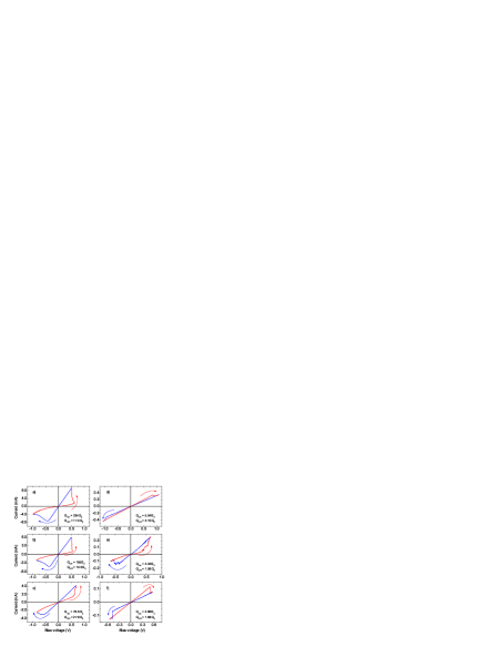
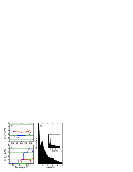
In this regime the I-V curves regularly exhibit a clear reversible switching behavior in the voltage range of V (more than of the junctions have shown jumps with relative amplitudes above ). Figure 1 shows typical I-V characteristics for contacts of various conductances. Both the current and voltage values seem to be surprisingly high for a device with dimensions of a few nanometers. The corresponding current densities exceed A/cm2. Note, however, that in this mesoscopic transport regime the contacts are not destroyed by the Joule heat, as the dissipation occurs inside a much larger volume determined by the inelastic scattering length Untiedt et al. (2000); Agraït et al. (2003).
A careful comparison of the curves shown in Fig. 1 reveals significant differences between the characteristics of the junctions with typical on-state conductance of (panels on the left) and that of the smaller contacts with on-state conductance below about (panels on the right). Junctions in the first, higher conductance regime will be denoted as nanoscale junctions. For such contacts, the current steeply increases as soon as a critical voltage is exceeded. The conductance, however, does not saturate at a predefined value, it increases as long as the applied voltage is ramped up. In our system a serial resistance of is present, which limits this process as the junction’s resistance becomes comparable to . Note, that in this regime the circuit is not purely voltage driven, which accounts for the back-turning of the I-V curve in Fig. 1 (a). We found, that in these nanoscale junctions the direction of the current-voltage loops is the same for all the curves.
In contrast, smaller junctions with – denoted as atomic-sized contacts – exhibit a switching behavior between different well defined initial and final states. During the switching event the system jumps to a new state, corresponding to a new line in the I-V characteristics, and stays there both for increasing and decreasing voltage ramps (until a back-switching occurs for reversed voltage). The switching voltage, however, scatters in a broad range. Moreover, the direction of the loops is random.
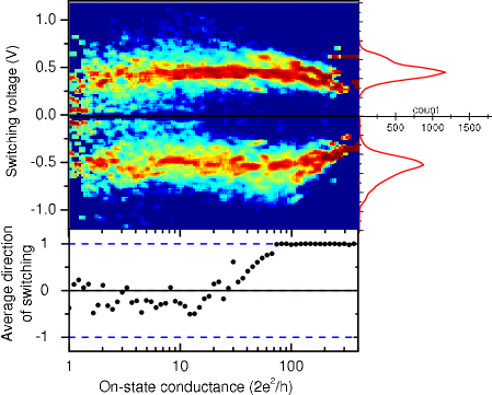
The above features, presented on selected curves, are confirmed by statistical analysis of a large amount of junctions. In Fig. 2 (a) the switching voltage values are shown in the form of a 2D colorscale plot. It is evident that for nanoscale junctions () the switching voltage has a relatively well defined value at both polarities around V, whereas for atomic-sized contacts () the switching voltage scatters randomly in a broad voltage region. An even more obvious distinction is observed in the direction of the switching. This is represented by value if the bias voltage of the sample is positive/negative with respect to the tip for the offon transition. Averaging the direction of the switching for various junctions with similar conductance, one finds that the switching is always positive for , whereas for the sign of the switching varies randomly (Fig. 2 (c)). We argue that the two distinguished switching mechanisms are related to fundamentally different physical phenomena. First we discuss the reproducible resistive switching observed in highly conducting contacts, and later we return to the random switching observed at the atomic level.
The curves recorded for nanoscale junctions are very similar to those recently reported for resistive switches based on Ag-Ag2S-Me sandwich structuresTerabe et al. (2002, 2005); Morales-Masis et al. (2009); Nayak et al. (2010), where Me is a transition metal and Ag2S is an ionic conductor layer formed between the two electrodes. The operation of these devices is based on the electrochemical reaction that is, the solubility of ions in the Ag2S lattice allows migration controlled by the bias voltage applied. For asymmetric contacts, reversible metallic filaments are built up and destructed by applying a negative/positive voltage, respectively, which is reflected by abrupt changes in the device conductance. The ionic migration is an activated processNayak et al. (2010) resulting in a threshold voltage bias. In our measurements the sign of the switching, the value of the threshold voltage and the overall shape of the curves are consistent with earlier experimentalTerabe et al. (2002, 2005); Morales-Masis et al. (2009); Nayak et al. (2010) and theoreticalRozenberg et al. (2004) reports on such ionic switches. We emphasize, however, that in our measurements no special treatment of the sample was performed, exposing the Ag layer to air for more than one week was enough to establish the ionic-type switching behavior. More details on sample characterization are provided in the supplementary material.
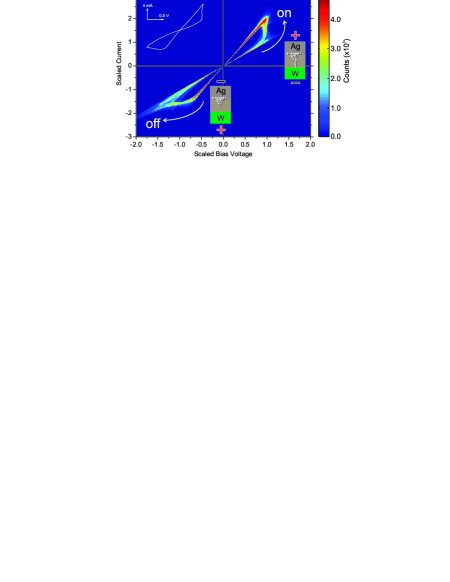
In order to demonstrate the universal and reproducible nature of this phenomenon we scaled the individual I-V curves recorded in the range from to by normalizing them to fixed, and zero bias conductance values. The resulting color density map – acquired out of more than independent I-V curves – is shown in Fig. 3 demonstrating that the character of the I-V curve is very similar for a broad variety of nanoscale junctions. It is notable that the branch of lower conductance exhibits more pronounced nonlinearity compared to the upper one indicating the tunneling nature Simmons (1963) of the low-conducting state, which is shunted when metallic filaments are formed. This distinction is even more clearly visible in Fig. 1 (a), (b) and (c). The different characters of the onoff and offon transition also show clear similarities to the results of earlier measurements Morales-Masis et al. (2009); Waser and Aono (2007); Morales-Masis et al. (2010).
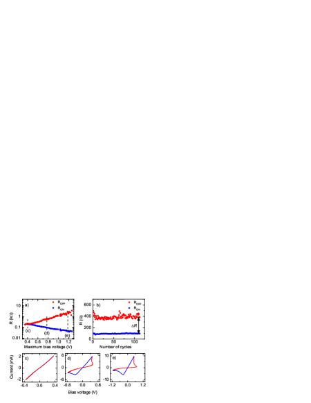
It was also studied how the states of the ionic switch can be tuned by the applied bias voltage. Figure 4 (a) demonstrates that both states can be altered considerably. For this particular junction, the onset of the resistive switching is at V. By gradually increasing the amplitude of the voltage ramp the on- and off-state resistance values are rapidly tuned. The larger the resistance ratio, the larger threshold is observed for the offon transition, which we attribute to a wider insulating gap formed between the metallic sample and the tip.
We found that for constant amplitude ramping the switching phenomenon shows excellent reproducibility. In this stationer state no apparent change is observed during more than cycles, as shown in Fig. 4 (b). This stability and reproducibility is characteristic of the ionic switching. Decreasing the contact diameter below about nm, however, results in a crossover to a fundamentally different switching phenomenon.
In case of the atomic-sized contacts the qualitative observations, especially the random switching sign and the broad range of the threshold voltages, contradict the picture of ionic switching. In this regime we attribute the switching process to atomic rearrangements in the junction due to electromigration induced by the high current density. The relevance of single atomic displacements is demonstrated in Fig. 5 (a) and (b), where typical switching traces are presented as conductance-voltage curves. Since the conductance value of a single Ag atom corresponds to the conductance quantum, (Ref. 15), jumps of this magnitude indicate the inclusion or removal of a single atom in the junction area. Multiple steps are often observed with amplitudes close to the integer multiplies of further supporting this scheme.
The role of the single atomic migration is also supported by the statistical analysis of a large number of switching characteristics. A histogram was made of the conductance traces detected during the voltage sweeps by subtracting the baseline conductance measured in a narrow window (mV) around zero bias. The result is shown in Fig. 5 (c). The well defined peak around reflects that relative jumps corresponding to single atom conductance are dominating. For comparison, the inset of Fig. 5 shows the traditional conductance histogram measured on the same sample by repeatedly indenting the tip to the surface and breaking the such created nanojunction at a constant bias voltage of mV.
In a control experiment the above phenomenon was investigated in the same voltage and current ranges utilizing the mechanically controllable break junction technique (MCBJ), where the junction is created by the in-situ breaking of a silver wire Agraït et al. (2003). The freshly broken surfaces created in cryogenic vacuum warrant the absence of ionic contamination in the junction. This method fully reproduced the main features of the switching characteristics observed for atomic scale contacts [Fig. 1 (d)-(f)], while those of larger junctions were not observed. Preliminary results obtained by the MCBJ technique on pure Au, Pt, Fe revealed that the current induced atomic switching is a quite general phenomenon in atomic-sized junctions.
In conclusion, we have identified two resistive switching mechanisms at the nanoscale. It was shown that the ionic conductor-based devices are good candidates for nonvolatile memory cells as they exhibit stable and reproducible switching behavior. It was demonstrated, that solely the exposure of an Ag thin layer to air is enough to establish an ionic conductor surface layer, which is sufficient to form a reliable switching device in a nanoscale point-contact geometry. Our results set lower limit for the size of such memory cells, below which the character of the switching process dramatically changes due to the enhanced single atomic migration. This size limit is estimated to be nm, resulting in storage densities above the capacity of current NAND Flash devices Kryder and Kim (2009) and comparable to the proposed bit size of magnetic media determined by the superparamagnetic limit Weller et al. (2000).
The authors are grateful to L. Bujdosó and E. Szilágyi for sample preparation and characterization. This work was supported by the New Hungary Development Plan under project ID: TÁMOP-4.2.1/B-09/1/KMR-2010-0002 and by the Hungarian Research Funds OTKA under grants No. 72916 and No. 76010. A. H. is a grantee of the Bolyai János scholarship.
References
- Terabe et al. (2005) K. Terabe, T. Hasegawa, T. Nakayama, and M. Aono, “Quantized conductance atomic switch,” Nature 433, 47–50 (2005).
- Kaeriyama et al. (2005) S. Kaeriyama, T. Sakamoto, H. Sunamura, M. Mizuno, H. Kawaura, T. Hasegawa, K. Terabe, T. Nakayama, and M. Aono, “A nonvolatile programmable solid-electrolyte nanometer switch,” Solid-State Circuits, IEEE Journal of 40, 168 – 176 (2005).
- Strukov et al. (2008) Dmitri B. Strukov, Gregory S. Snider, Duncan R. Stewart, and R. Stanley Williams, “The missing memristor found,” Nature 453, 80–83 (2008).
- Waser and Aono (2007) Rainer Waser and Masakazu Aono, “Nanoionics-based resistive switching memories,” Nature Mater 6, 833–840 (2007).
- Linn et al. (2010) Eike Linn, Roland Rosezin, Carsten Kugeler, and Rainer Waser, “Complementary resistive switches for passive nanocrossbar memories,” Nature Mater 9, 403–406 (2010).
- Yang et al. (2008) J. Joshua Yang, Matthew D. Pickett, Xuema Li, A. Ohlberg, Douglas A., Duncan R. Stewart, and R. Stanley Williams, “Memristive switching mechanism for metal/oxide/metal nanodevices,” Nature Nanotech 3, 429–433 (2008).
- Dietrich et al. (2007) S. Dietrich, M. Angerbauer, M. Ivanov, D. Gogl, H. Hoenigschmid, M. Kund, C. Liaw, M. Markert, R. Symanczyk, L. Altimime, S. Bournat, and G. Mueller, “A nonvolatile 2-Mbit CBRAM memory core featuring advanced read and program control,” Solid-State Circuits, IEEE Journal of 42, 839–845 (2007).
- Dong et al. (2008) Yajie Dong, Guihua Yu, Michael C. McAlpine, Wei Lu, and Charles M. Lieber, “Si/a-Si core/shell nanowires as nonvolatile crossbar switches,” Nano Letters 8, 386–391 (2008).
- van der Molen and Liljeroth (2010) Sense Jan van der Molen and Peter Liljeroth, “Charge transport through molecular switches,” Journal of Physics: Condensed Matter 22, 133001 (2010).
- Kryder and Kim (2009) M.H. Kryder and Chang Soo Kim, “After hard drives: What comes next?” Magnetics, IEEE Transactions on 45, 3406–3413 (2009).
- Landauer (1970) R. Landauer, “Electrical resistance of disordered one-dimensional lattices,” Phil. Mag. 21, 863–867 (1970).
- Scheer et al. (1998) Elke Scheer, Nicolas Agraït, Juan Carlos Cuevas, Alfredo Levy Yeyati, Bas Ludoph, Alvaro Martin-Rodero, Gabino Rubio Bollinger, Jan M. van Ruitenbeek, and Cristian Urbina, “The signature of chemical valence in the electrical conduction through a single-atom contact,” Nature 394, 154–157 (1998).
- Sharvin (1965) Y. U. Sharvin, “A possible method for studying Fermi surfaces,” Sov. Phys. JETP 21, 655–656 (1965).
- Untiedt et al. (2000) C. Untiedt, G. Rubio Bollinger, S. Vieira, and N. Agraït, “Quantum interference in atomic-sized point contacts,” Phys. Rev. B 62, 9962–9965 (2000).
- Agraït et al. (2003) Nicolás Agraït, Alfredo Levy Yeyati, and Jan M. van Ruitenbeek, “Quantum properties of atomic-sized conductors,” Physics Reports 377, 81 – 279 (2003).
- Terabe et al. (2002) K. Terabe, T. Nakayama, T. Hasegawa, and M. Aono, “Ionic/electronic mixed conductor tip of a scanning tunneling microscope as a metal atom source for nanostructuring,” Applied Physics Letters 80, 4009–4011 (2002).
- Morales-Masis et al. (2009) M. Morales-Masis, S. J. van der Molen, W. T. Fu, M. B. Hesselberth, and J. M. van Ruitenbeek, “Conductance switching in Ag2S devices fabricated by in-situ sulfurization,” Nanotechnology 20, 095710 (2009).
- Nayak et al. (2010) Alpana Nayak, Takuro Tamura, Tohru Tsuruoka, Kazuya Terabe, Sumio Hosaka, Tsuyoshi Hasegawa, and Masakazu Aono, “Rate-limiting processes determining the switching time in a Ag2S atomic switch,” The Journal of Physical Chemistry Letters 1, 604–608 (2010).
- Rozenberg et al. (2004) M. J. Rozenberg, I. H. Inoue, and M. J. Sánchez, “Nonvolatile memory with multilevel switching: A basic model,” Phys. Rev. Lett. 92, 178302 (2004).
- Simmons (1963) John G. Simmons, “Generalized formula for the electric tunnel effect between similar electrodes separated by a thin insulating film,” Journal of Applied Physics 34, 1793–1803 (1963).
- Morales-Masis et al. (2010) Monica Morales-Masis, Hans-Dieter Wiemhofer, and Jan M. van Ruitenbeek, “Towards a quantitative description of solid electrolyte conductance switches,” Nanoscale 2, 2275–2280 (2010).
- Weller et al. (2000) D. Weller, A. Moser, L. Folks, M.E. Best, Wen Lee, M.F. Toney, M. Schwickert, J.-U. Thiele, and M.F. Doerner, “High Ku materials approach to 100 Gbits/in2,” Magnetics, IEEE Transactions on 36, 10–15 (2000).