Size and Defect related Broadening of Photoluminescence Spectra in ZnO:Si Nanocomposite Films
Abstract
Nanocomposite films of Zinc Oxide and Silicon were grown by thermal evaporation technique using varying ratios of ZnO:Si in the starting material. Analysis reveal the role of ZnO and amorphous silicon interface in contributing to relatively less common blue photoluminescence emissions (at 400 and 470nm). These blue peaks are observed along with the emissions resulting from band edge transition (370nm) and those related to defects (522nm) of ZnO. Careful analysis shows that along with the grain size of ZnO, a suitable compositional ratio (of ZnO to silicon) is critical for the coexistence of all the four peaks. Proper selection of conditions can give comparable photoluminescence peak intensities leading to broad-band emission.
Keywords Nano-composites, Nanostructures, Photoluminescence, Oxides
1 Introduction
Recent research in Material Science is directed along the lines of tailoring material properties as per requirement. In this direction both materials in nano regime and in composite state has drawn attention. Interest hence has also been developed in materials in nanocomposite state. Nanocomposites by defintion refer to the class of composite materials wherein atleast one of the constituents exists in the nanometre range. Research on ZnO based nanocomposites has been a front-runner in recent times, especially in the field of white light emitting devices (LED) [1, 2]. These nanocomposites enjoy two-fold advantage over ZnO nanomaterials. While a carefully selected host material can result in broadening of light emission, it also gives additional stabilty to the ZnO film and prevents agglomeration of the grains. Of all the possible hosts, the research is mainly centred around the use of silicon and its varied complexes [3, 4, 5, 6, 7, 8]. This is because of the key position of silicon in the microelectonic industry and its abiliy to emit in the red region in the nanophase.
In quest for obtaining white light, Klason et al [9] have tried depositing n-type ZnO nanorods on p-Si, which emitted white light under forward biasing. Depositing of ZnO nanoparticles in porous silicon (po-Si) has also been reported by Bo et al [10] and Mehra et al [11]. Though the intensity of luminescence observed in Bo’s work was high, use of porous Si substrate itself suffers from the demerit of being prone to quick oxidation and requires tedious method of production. Peng [12] and Pal [13]had studied the effect of varying ZnO to silicon content. Peng et al [12] were successful in obtaining white light from RF sputtered films with the lowest ZnO content (26% of ZnO). By considering the role of heterogeneous boudaries and taking into account the depletion width thus developed, they explained the maximum obtained intensity of the blue photoluminescence (PL) peak observed in the samples with lowest Zinc Oxide nanoparticles. In a later work [14] they also discussed the color chromaticity dependance on the dot diameter. With their work they were able to prove that the neighbourhood and the size of the ZnO grains are both important for the efficient white light production. Using a similar method of fabrication Pal et al tried dispersing Si atoms in ZnO matrix. The samples were then annealed at high temperature. An increase in PL intensity was observed upon annealing and with decrease of ZnO content in the films. Unlike the PL behavior reported by Peng, the intensity in Pal’s samples decreased with further lowering of ZnO content of the films. Thus it becomes clear that the compositional ratio of ZnO to Silicon which inturn means the neighbourhood offered to ZnO nanoparticles is deterimental in bringing desired changes in optical properties of the nanocomposites and should be given its due concern. Nanocomposites based on ZnO and Si have been fabricated by sol gel [15, 16, 17, 18, 19], RF sputtering [20, 21, 22, 23], pulsed laser deposition [24], via chemical routes [25, 26, 27, 28], reverse micelle method [29]and their optical properties studied. These research calls for more systematic work to optimize the parameteres for tailoring the properties and for a better understanding of interface and defect mechanism of ZnO:Si nanocomposites
Hence to this effect, we have started systematic study of Zinc Oxide grains in nano regime embedded in amorphous Silicon matrix. In our earlier work,[30] we had demonstrated that these films emitted light in the visible region, namely in UV, blue, green and red regions. To investigate the tailoring of our samples’ properties, we annealed our samples (post deposition) and reported broadening of photoluminescence emissions. Not only this, the intensity of the annealed samples increased manifold [31]. In this manuscript we report the role of varying ratio of ZnO:Si (in starting material) on the photoluminescence.
2 Experimental Details
The films of ZnO:Si nanocomposites studied in this work were fabricated by thermally evaporating a mixture of powdered ZnO and n-Silicon. Vacuum of the order of Torr was created in the deposition chamber of a Hind High Vac (Bengaluru), Thermal evaporation coating unit, Model 12A4D. The deposition was carried out on microcopic glass substrates maintained at room temeprature. To prevent the flying off, of starting material powdered ZnO and Si, was pelletized by applying a pressure of 60kN. ZnO used in this study was(99.99 %) pure and purchased from Merck (Mumbai). The mixture was prepared by mixing ZnO and Silicon in the proportions of 1:1, 1:2, 1:3, 2:3 and 2:5 (by weight). Films of these composition are hereafter referred to as sample (a), (b), (c), (d) and (e), respectively. We have restricted the present study to samples of 600Å thickness. The samples discussed in this work are as grown, not subjected to any post deposition heat treatment.
The structural studies of the surface is measured by Pananalytical PW3050/60 Grazing Incidence angle X-Ray Diffractometer (GIXD) and that of the bulk region by Philips PW 3020 X-Ray Diffractometer (XRD). X-Ray Photoelectron Spectroscopy (XPS) was performed with Perkin-Elmer X-ray Photo-electron Spectrometer (Model 1257) with Mg (1254 eV) X-ray source. Photoluminescence (PL) scans were recored on Jobin Yvon spectroscopes respectively. Renishaw’s “Invia Reflex” Raman spectroscope was used for measurements. The surface morphology and texture of the as grown nanocomposite films were studied using the Scanning Electron Microscope (SEM), atomic force microscopy (AFM)- NTEGRA NS-150 and Transmission Electron Microscope (TEM). In the following section we enlist the results of the various analysis done on our samples.
3 Results and Discussions
3.1 X-Ray Diffraction, Chemical Composition & Morphological Studies
The nanocomposite films were fabricated by co-evaporating Zinc Oxide with Silicon. The melting point of silicon is at atmospheric pressure while that of Zinc Oxide is about . However, the melting point of Zinc Oxide is known to reduce in the presence of group-IV elements facilitating its thermal evaporation at a lower temperature [32, 33, 34]. Both these materials have diverse melting points which could result in multilayered structure rather than a homogeneous nanocomposite film. The possibility of formation of multilayered structure was overruled by IR analysis of the films which was reported in our earlier work [30].
We have further tried to resolve this question using grazing incidence angle X-Ray diffraction studies (GIXD). At critical incidence angle, usually lying between and , the X-ray beam gets totally reflected from the surface. Infact below the critical angle, the reflected beam is allowed to penetrate only upto few nanometres [35, 36, 37, 38]. This ensures X-Ray is being diffracted from the surface layer. Figure 1A exhibits the nature of the diffraction pattern obtained for films of the same thickness but varying ratios of Zinc Oxide to Silicon. These X-Ray diffraction pattern show prominent peaks at , and . These peaks correspond to pure Zinc (ASTM Card No-4-831). The peak can possibly be unresolved peak of Zinc and Zinc Oxide (ASTM Card No-1451). The existence of elemental Zinc as shown by GIXD would imply that the surface of our films have metallic Zinc. This may not be the case within the surface of the films. To investigate this we have also studied the same samples using X-Ray diffraction studies. The results are shown in figure 1B. Barring sample (a) corresponding to the 1:1 ratio film, the X-Ray diffraction pattern of all the other samples were unmarked. This did not come as a surprise since the grain size of ZnO in nanocomposite films of is too small to result in X-Ray diffraction [30, 39].
In short, our X-Ray analysis suggests formation of pure Zinc on the surface of nanocomposite bulk, where Zinc Oxide is embedded within the matrix of Silcon. To investigate the depth to which elemental Zinc exist, we have analysed sample (a) using XPS. XPS scans were made at the surface and periodically repeated after removing layers of 100Å by ion milling. Figure 2A shows the Zinc 1022eV peak associated with it orbital. Figure 2A compares the Zinc peaks as scanned at depths of 100, 200, 300, 400 and 500Å. These are single peaks which show a shift to lower energy side with increasing depth. However, as can be seen from Figure 2B, the Zinc peak from the surface layer can be deconvoluted into two peaks. The peaks are separated by 1eV. The 1021eV is associated with free Zinc or Zinc atoms which are not in bonding with any other species [40, 41, 42, 43, 44], while the 1022eV peak shows that there are sizeable amount of Zinc atoms that present in bonding with oxygen, existing as Zinc Oxide [40, 41]. To colloborate this, we have also scanned the layers for oxygen.
Figure 2C compares the oxygen peaks along the thickness of the film. Here also, oxygen seems to exist in two chemical compositional states as is indicated by the deconvoluted peaks shown in the figure. The only possibility is oxygen in bonding with Zinc and Silicon present in the film. The 530.5eV peak of the surface layer, corresponds to oxygen in bonding with Zinc, confirming that the surface of sample (a) has Zinc and Zinc Oxide. A close look of Figure 2C, reveals that the oxidation of silicon at the surface has not passivated the surface and protected the inner layers completely, as can be understood by the presence, abid diminishing contribution of the 532eV peak. This could be because the sample in question is of small thickness and the XPS scanning was done after a long time from its date of fabrication. Figure 2D exhibiting Si XPS peaks, also confirms the existence of Silicon and Silicon dioxide in the film with the deconvoluted peaks clearly observable through the entire thickness of the sample (a). This establishes that our film contain Zinc Oxide embedded in a matrix of Silicon and Silicon Dioxide with elemental Zinc at the surface. However, it must be emphasised again that the occurrence of silicon dioxide only took place after a long time from the sample’s fabrication time.
Before proceeding it is worth mentioning again that the Zinc XPS peak corresponding to atoms in bonding with oxygen shifts with their position along the depth of the film. Figure 3 shows the near linear trend with this peak moving from 1022.4eV at the surface to 1021.8eV within the film. We beleive this shift in peak as you go within the thickness of the film is due to the chemical species and it’s relative quantity existing around the ZnO molecules. Figure 3B clearly shows increase in relative Zinc Oxide as you move deeper into the film. It should be noted that our starting material for sample (a) had 50% ZnO however as can be anticipated, the film’s bulk only has 24-30% ZnO. Figure 3C combined the best fit curves of Figure 3A and 3B and projects variation in peak position as ZnO percentage varies. Larger amount of Silicon seems to shift the ZnO peak to the higher energy side. This is the precise influence we are investigating and hope would assist in tailoring the optical properties of these nanocomposites. Also, we expect the same trend of Figure 3C for samples prepared with differnt ZnO presence. We are in process of studying samples with different starting ratios, same thickness and verifying this.
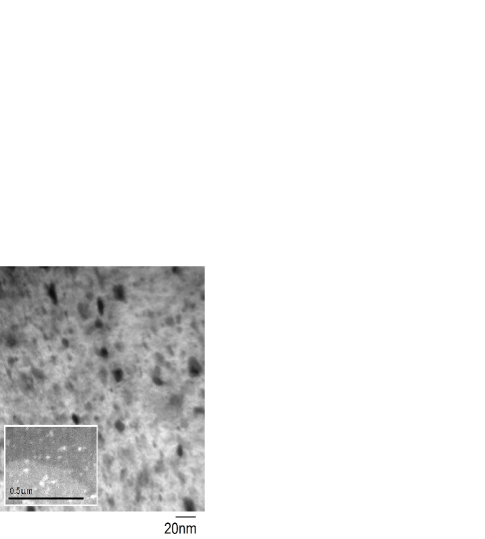
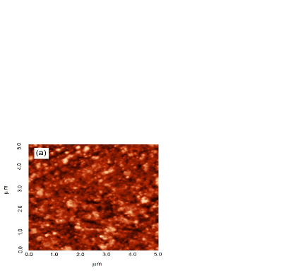
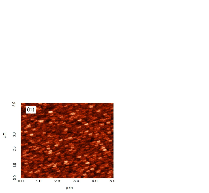
TEM micrograph (Figure 4) of sample (c) shows existence of two phases. The clusters of ZnO dispersed in a matrix of amorphous Silicon. The inset shows image taken in dark field which brings better contrast. For studying the film-morphology we carried out AFM analyis on the sample surface. The AFM images of the samples (a) and (b) are shown in Figure 5A and 5B, respectively. The AFM images reveal uniform films with particles ranging in nanometre. However, while discussing the X-Ray analysis results, we have clearly established the existence of elemental Zinc on the surface of the films hence, the observed grains and measured grain size are not typically of ZnO. Hence, the grain size of ZnO was also calculated using the Debye-Scherrer formula [45] from the peak of GIXD. The grain size of ZnO was found to lie between 8.8 to 23nm for our samples.
Along with the nature of Zinc Oxide’s neighbouring chemical composition and it’s grain size, it is understood that the strain acting on Zinc Oxide lattice also contributes to its optical properties. The ZnO peak in XRD is only observed in one sample (that of ‘a’, see Figure 1B). There is a distinct right shift in the observed peak position with respect to the peak position reported for a single crystal. This shift is indicative of a tensile stress. We have calculated the strain from which stress can be calculated [45]. Strain is usually evaluated using [45]
| (1) |
where is the ‘d’ spacing for the single crystal structure and is that for the sample in question. Using equation (1) the strain within the bulk of sample (a) is found to be . As expected, this is different from strain acting on the surface, which was found to be . However, since the order is same we can consider strain acting on surface is representative of that in the bulk. The surface strain was found to be decreasing with decreasing ZnO presence in the films. The tensile strain detected is due to the defects caused by vacancies [46]. This can also be appreciated from Raman spectra. Hence, we analysed our samples using Raman Spectra. The results of our study is discussed below.
3.2 Raman Spectra
The Raman spectra were taken in standard back scattering geometry using laser for excitation. Figure 6 gives the Raman spectra for the sample (a), (d), (b), (e) and (c) respectively. Broad peaks were obtained from to . These peaks were deconvoluted to give three peaks. We are confident about our deconvolution at and because of the prominent shoulders they give. The peak corresponds to the LA mode of amorphous Silicon [30, 51]. The intensity and contribution of this peak to the Raman spectra is indicative of the amorphous Silicon in our samples. The large Silicon shown in Raman analysis which were carried out soon after the fabrication confirms our arguement that Silicon Oxide (shown in XPS) formed with time.
The corresponds to the A1 LO peaks of ZnO which is essentially associated with defect structures in ZnO. This defect in literature has been associated to either Oxygen vacancies or Zinc interstitial defects [47]. From our X-Ray analysis on we reported vacancies giving rise to tensile strain. Hence, we beleive this peak is due to Oxygen vacancies in our samples. This is ofcourse expected to influence the optical properties of the samples. The third peak is at . Although the position of this deconvoluted peak may not be as reliable as the other peaks because of the lack of prominent shoulders, this can be ascribed as the peak of ZnO. The peak at is of mode of Zinc Oxide, usually reported at [48, 49, 50] and possibly merged with amorphous Silicon that is expected at [51, 52, 53]. The peak is related to the vibration of the oxygen atom in the wurtzite structured ZnO lattice. The presence of this huge peak in all the samples further confirms the presence of ZnO in the bulk region of the films. The existence of reconfirms our claim of ZnO being embedded in the amorphous Silicon.
It is clear from the Raman Spectra that our nano-composite samples is not just ZnO clusters dispersed in a matrix of amorphous Silicon but additionally the ZnO cluster is a homogeneous mix of lattice with perfect wurzite crystallinity and that with oxygen defects. Considering that the optical properties of ZnO strongly depends on it’s structure giving PL emission at 520 or 370nm depending on existence of defects or good crystallinity, existence of both phases in our sample should result in both peaks occuring in our PL. Thus, a suitable ratio of the contents of these two phases should give rise to a broad emission in the PL. Before looking at PL, we plot the ratio of area enclosed by the Raman peaks at and with respect to the content of ZnO in the film (fig 7). Figure 7 shows that the two areas are comparable in samples (b), (d) and (e). Hence, we expect the PL emission peaks at 370 and 520nm to be comparable in these three samples. In our next section we shall investigate these issues.
3.3 Photoluminescence
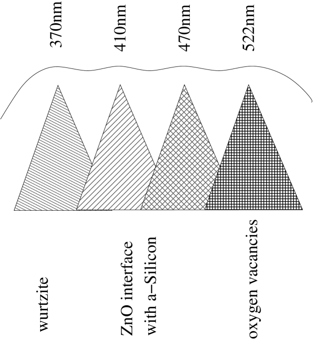
To study how the above discussed strcutural and compositional behaviour manifests in the optical properties we have studied the PL spectroscopy of our samples using an excitation source of Xenon lamp. The PL was scanned in the range of 290-800nm on excitation with wavelength of 270nm. Since the measurements were taken up without the use of filters, the presence of second harmonics at 540nm is inevitable and can be seen as line spectra along with the PL peaks (Figure 8). The PL of samples (a), (b), (c) and (d) exhibit similar behavior with four prominent peaks. There is a sharp peak at 370nm accompanied by broad peaks at 410nm, 470nm and 522nm. The 370nm is due to the radiation resulting from electron transistion across the band gap of Zinc Oxide [1, 2]. The 522nm is well documented [54, 55, 56] and is related to intra-band transistions, i.e. between levels created by defects within the band gap, caused by the Oxygen vacancies. As discussed in the Raman analysis, we had predicted broadening of emission spectra in samples (b), (d) and (e) because they had nearly equal amount of ZnO lattice with and without defects. The expected broadening is evident in our PL (fig 8).
Broadening is also assisted in our PL due to additional peaks at 410 and 470nm. The 414nm peak have been attributed to inter-grain boundary defects [31] in ZnO. However, over the large amount of samples we have studied we have observed that the 410 and 470nm peaks appear only if the background is a-Si. These peaks were absent in samples with n-Si background [30]. Hence, we propose that these peaks are indeed influenced by the intergrain boundary and the background species rather than, if not only by the defects. To further our idea, we argue that if these peaks are contributed by interface and hence by the net surface area of the ZnO grains, then the peak intensity would be a result of the grain size and number of grains present. This ofcourse is the underlying principle of nanotechnology. Assuming the number of grains in the film (N) to be proportional to the ratio of ZnO present in the starting material and using the grain size(R) evaluated using debye-Scherrer equation, we plotted a curve between the peak intensity of 465nm with (fig 9). We find this to be linear suggesting its dependence on the interface of ZnO and amorphous Silicon.
Similar correlation is found among results of other analysis. For example, the 522nm PL peak arises due to oxygen vacancy defects. The defects also manifest as strain in the film as seen by the displacement of XRD peak from expected position. The perfect linear relation between the area of the green PL peak with strain in samples, (fig 9b) confirm our inferences. The omission of the 365nm peak also shows proportionality with amount of wurtzite species present as seen from Figure 9(c) which plots area under 365nm peak of PL with respect to peak from Raman spectra. We can thus summarise that a sample with appropriate mixture of defects and defect free ZnO, grown with a starting material of 1:2 ZnO to Silicon with grains in nano regime would give four emission peaks that overlap. The overlapping results in broadening best understood by a schematic shown in Figure 10.
4 Conclusion
We have fabricated nanocomposite films of ZnO and Si using thermal evaporation technique with clusters of ZnO dispersed in a matrix of amorphous Silicon. Depth profiling ESCA scans along with earlier IR studies confirm formation of our nano-composite films. The PL of the samples shows four prominent peaks in the blue-green region, namely 400, 470, 370 and 522nm. The latter peaks are attributed to emissions via transistions from the band edge and defect related peaks from ZnO. On the other hand the 400 and 470nm peaks exist because of the interface between ZnO grains and amorphous silicon. The interface increases with decreasing grain size and increasing number of ZnO grains. This was established from the observation of varying PL intensity with varying the ZnO:Si compositional ratio and grain size. Samples with appropriate mixture of defects and defect free ZnO nanostuctures lead to broadening due to merging of peaks. We have found the 1:2 sample with maximum broadening. This sample with 22.4nm grain size also gave rise to large 465nm peak in PL indicating formation of large interfacial boundary. It thus proves, that not only the grain structure but also the interfacial boundaries and the nature of background species play a decisive role in equalizing the intensity accompanied by the broadening of the PL peaks. At present, we only observe a weak red emission and hope to control and improve the intensity of this peak. Enhancement and ultimately merging of red peak with the remaining emission spectra would estiblish ZnO:Si nano-composites as potential candidate for the development of cost effective white light emitting diodes.
Acknowledgment
The resources utilized at Indian Institute of Technology, Delhi and Geology Department, University of Delhi is gratefully acknowledged. Also, the resources used at the Instrumentation Center and University Information Resource Center, Guru Gobind Singh Indraprasta University is also acknowledged. We also would like to express our gratitude to Dr. Kamal Sanan and Dr. Mahesh Sharma (both at National Physical Lab., Delhi) for carrying out the photoluminescence and XPS studies respectively. Authors PA and CRK are thankful to University Grants Commission (India) for financial assistance in terms of Major Research Award, F.No-33-27/2007(SR).
Figure Captions
-
1.
X-Ray Diffractograms of sample (a),(b),(c),(d) and (e) obtained by (A) GIXD and (B) - technique.
-
2.
(A) XPS peaks of Zinc taken at various depth of same sample showing two species, (B) surface scan, (C) depth profile scans for Oxygen and (D) Silicon.
-
3.
Variation of (A) Peak position of Zn with depth (B) Fraction of Zinc in bonding with Oxygen to amount of Silicon present along the thickness and (C) Peak position of Zinc in bonding with Oxygen to its fraction of presence.
-
4.
TEM of sample (c). Inset shows dark field image of same sample taken at low magnification which clearly shows formation of two phase with ZnO clusters embedded in amorphous silicon.
-
5.
AFM images of sample (a) and sample (b).
-
6.
Raman spectra of sample (a), (d), (b), (e) and (c). Also seen are deconvoluted peaks assigned to amorphous silicon, wurtzite structure ZnO and with oxygen vacancies defects.
-
7.
Relative presence of ZnO with oxygen vacancies to wurtzite structure ZnO (Area /Area from Raman spectra) for varying ZnO content in film.
-
8.
PL of sample (a), (d), (b), and (c). Alongside the raw spectra are shown, deconvolution give 365, 400 and 465nm between 300 and 480nm. Also green emission due to defects have been separated from harmonic to show relative contributions.
-
9.
The (A) increase in contribution of 465nm PL peak with increasing , (B) linear relation in green (522nm) emission with strain in film and inturn oxygen vacancies and (C) co-relation in existence of wurtzite peak ( in Raman spectra) and blue emision (365nm peak of PL) in samples.
-
10.
Schematic explaining broadening of PL in ZnO:Si nanocomposites and their individual contributions.
References
- [1] C. Jagadish and S. J. Pearton, “Zinc Oxide Bulk, Thin Films and Nanostructures, Elsevier Ltd.”, 2006.
- [2] U. Ozgur, Ya. I. Alivov, C. Liu, A. Teke, M. A. Reshchikov, S. Dogan, V. Avrutin, S.-J. Cho and M. Morkoc, J. Appl. Phys., 98 (2005) 041301.
- [3] A.K.Das, P.Misra and L.M.Kukreja, J.Phys. D:Appl. Phys.,42 (2009) 165405.
- [4] B.Yang, A.Kumar, H.Zhang, P.Feng, R.S.Katiyar and Z.Wang, J.Phys. D:Appl. Phys.,42 (2009) 045415.
- [5] W.J.Shen, J.Wang, Q.Y. Wang, Y.Duan and Y.P. Zheng, J.Phys. D:Appl. Phys.,39 (2006) 269.
- [6] E.Bohmer, F.Siebke and H.Wagner, Fresenius J.Anal.Chem, J.Phys. D:Appl. Phys.,358 (1997) 210.
- [7] Q.Jiang, Zheng Ying Wu, Yi Meng Wang, Yi Cao, Chun Fang Zhou and Jian Hua Zhu, J.Mater.Chem., 16 (2006) 1536.
- [8] P.Cheng, D.Li and D.Yang, Optics Express, Vol.16, No.12 (2008) 8898.
- [9] P. Klason, P. Steegstra, O. Nur, Q-H. Hu, M. M. Rahman, M.Willander and R. Turan, Proceedings: “ENS 2007, Paris: France (2007)”.
- [10] ZHAO Bo, LI-Q-S, Qi H-X and ZHANG N, Chin Phys.Lett., 23 (2006) 1299.
- [11] R. G. Singh, Fouran Singh, V. Aggarwal and R. M. Mehra, J.Phys. D: Appl. Phys., 40 (2007) 3090.
- [12] Yu-Yun Peng, Tsung-Eong Hseih and Chia-Hung Hsu, Nanotechnology, 17 (2006) 174.
- [13] U. Pal, J. Garcia Serrano, N. Koshizaki and T. Sasaki, Mater. Sci. Eng. B, 113 (2004) 24.
- [14] Yu-Yun Peng, Tsung-Eong Hseih and Chia-Hung Hsu, App.Phys.Lett., 89 (2006) 211909.
- [15] M.Bouguerra, M.Samah, M.A.Belkhir, A.Chergui, L.Gerbous, G.Nouet, D.Chateigner and R.Madelon, Chem. Phys. Lett., 425 (2006) 77.
- [16] S.Chakrabarti, D.Ganguly and S Chaudhuri, J.Phys. D:Appl. Phys.,36 (2003) 146.
- [17] Mikrajuddin, F.Iskandar, K.Okuyama and F.G.Shi, J.Appl.Phys., Vol. 89, No. 11 (2001) 6431.
- [18] S.Chakrabarti, D.Das, D.Ganguly and S.Chaudhuri, Thin Solid Films,441 (2003) 228.
- [19] Z.Fu, B.Yang, Lin Li, W.Dong, C.Jia and W.Wu, J.Phys.:Condens. Mater, 15 (2003) 2867.
- [20] J.G.Ma, Y.C.Liu, C.S.Xu, Y.X.Liu, C.L.Shao, H.Y.Xu, J.Y.Zhang, Y.M.Lu,D.Z.Shen and X.W.Fan, J. Appl. Phys., 97 (2005) 103509.
- [21] Z.D.Sha, Y.Yan, W.X.Qin, X.M.Wu and L.J.Zhuge, J.Phys. D:Appl. Phys.,39 (2006) 3240.
- [22] U.Pal, N.Koshizaki, Shin-ya Terauchi and T.Sasaki, Microsc. Microanal. Microstruct, 8 (1997) 403.
- [23] G.Mayer, M.Fonin, U.Rudiger, R.Schneider, D.Gerthsen, N.Janben and R. Bratschitsch, Nanotechnology, 20 (2009) 075601.
- [24] Y.Zhu, H.Wang and P.P.Ong, J.Phys.:Condens. Mater, 13 (2001) 787.
- [25] B.Yao, H.Shi, H.Bi and L.Zhang, J.Phys.:Condens. Matter, 12 (2000) 6265.
- [26] Y.L.Liu, Y.C.Liu, H.Yang, W.B.Wang, J.G.Ma, J.Y.Zhang, Y.M.Lu, D.Z.Shen and X.W.Fan, J.Phys.D:Appl.Phys., 36 (2003) 2705.
- [27] J.M.Yuk, J.Y.Lee, J.H.Jung, D.U.Lee, T.W.Kim, D.I.Son and W.K.Choi, J.App. Phys., 103 (2008) 083520.
- [28] L.Fernandez, N.Garro, J.Haskouri, M.Perez-Cabero, J.Alvarez-Rodriguez, J.Latorre, C.Guillem, A.Beltrain, D.Beltran and P.Amoros, Nanotechnology, 19 (2008) 225603.
- [29] C.Bouvy, W.Marine and B.Su, Chem. Phys. Lett., (2005), doi:10.1016/j.cplett.2007.02.061.
- [30] Shabnam Siddiqui, Chhaya Ravi Kant, P. Arun and N.C. Mehra,Phys. Lett. A, 372 (2008) 7068.
- [31] Shabnam, Chhaya Ravi Kant and P. Arun, Mater. Res. Bull. (2010), doi:10.1016/j.materresbull.2010.06.049.
- [32] LI Hong-Dong, LU Hang, SANG Dn-Dan, LI Dong-Mei, LI Bo, LU Xian-Yi and ZOU Guang-Tian, Chin. Phys. Lett., Vol.25, No. 10 (2008) 3794.
- [33] B.D.Yao, Y.F.Chan and N.Wang, App. Phys. Lett., Vol.81, No.4 (2002) 757.
- [34] K.Kongjai, D.Srisongrach, N.Mangkorntong, P.Mangkorntong and S.Choopun, CMU.J.Nat.Sci., Vol.7, No. 1 (2008) 37.
- [35] S.A.stepanov, E.A. Kondrashkina, R.Kohler, D.V.Novikov, G.Materlik and S.M.Durbin, Phys.Rev.B, Vol.57, No.8 (1998) 4829.
- [36] B.K.Tanner, T.P.A.Hase, T.A.Lafford and M.S.Goorsky, JCPDS-international Centre for Diffraction Data 2004, Advances in X-Ray Analysis, Vol.47 (2004) 309.
- [37] Pulak Dutta, Current Science, Vol.78 No.12 (2000) 1478.
- [38] D.W.Breiby, O.Bunk, J.W.Andreasen, H.T.Lemke and M.M.Nielsen, J.Appl.Cryst., Vol.41 (2008) 262.
- [39] Gwo-Mei Wu and Chen-Yen Wu, Cryst. Res. Technol., 42 (2007) 1271.
- [40] C. D Wagner, W. M Riggs, L. E Davis, J. F Moulder and G. E Muilenberg,“Handbook of X-ray photo-electron spectroscopy”, Perkin-Elmer Corporation, Physical Electronics Division (1978).
- [41] D. Briggs, “Handbook of X-ray and Ultra-violet Photon-electron Spectroscopy”, Heyden (London, 1977).
- [42] J.Liqiang, Y.Fulong, H.Haige, X.Baifu, C.Weimin and F. Honggang, Sci in China Ser.B Chem. Vol.48 No.1 (2005) 25.
- [43] F.Ren, C.Z.Jiang and X.H.Xiao, Nanotechnology, 18 (2007) 285609.
- [44] X.H.Wang, S.Liu, P.Chang and Y.Tang, Chin.J.Chem.Phys., Vol.20 No.6, (2007) 632.
- [45] “ Elements of X-Ray Diffraction” B.D.Cullity (London,1959).
- [46] FU Zhu-xi, Guo chang-xin, LIN Bi-xia and LIAO Gui-hong, Chin.Phys.Lett., Vol.15 No.6, (1998) 457.
- [47] C.X.Xu, X.W.Sun, B.J.Chen, P.Shum, S.Li and X.Hu, J.Appl.Phys.,Vol.95, No.2 (2004) 661.
- [48] Ramon Cusco, Esther Alarcon-Llado, Jordi Ibanez, Luis Artus, Juan Jimenez, Buguo Wang, and Michael J. Callahan, Phys. Rev. B 75 2007) 165202.
- [49] K.A.Alim, V.A.Fonoberov and A.A.Balandin, J.Appl.Phys., 97 (2005) 124313.
- [50] T. C. Damen, S. P. S. Porto and B. Tell, Phys. Rev. 142(1966) 570.
- [51] M. M. Khayyat, Godsway K. Banini, D. G. Hasko and M. M.Chaudhri, J. Phys. D: Appl Phys., 36 (2003) 1300.
- [52] Y. He, L. Bi, J. Y. Feng and Q. L. Wu, J. Phy D: Appl.Phys., 39 (2006) 449.
- [53] Chandan Biswas, S. N. Ghosh and C. S. Solanki, Proceedings:“Advances in Energy Research (2006)”.
- [54] F.H.Leiter, H.R.Alves, A.Hofstaetter, D.M.Hofmann and B.K.Meyer, Phys.Stat.Sol., 226, No.1 (2005) R4-R5.
- [55] S.A.Studenikin, Nickolay Golego and Michael Cocivera, J.Appl.Phys., 84, No.4 (1998) 2287.
- [56] R. B. M Cross, M. M. De Souza and E. M. Sankara Narayanan, Nanotechnology 16 (2005) 2188.