Enhancing the optical excitation efficiency of a single self-assembled quantum dot with a plasmonic nanoantenna
Abstract
We demonstrate how the controlled positioning of a plasmonic nanoparticle modifies the photoluminescence of a single epitaxial GaAs quantum dot. The antenna particle leads to an increase of the luminescence intensity by about a factor of eight. Spectrally and temporally resolved photoluminescence measurements prove an increase of the quantum dot’s excitation rate. The combination of stable epitaxial quantum emitters and plasmonic nanostructures promises to be highly beneficial for nanoscience and quantum optics.
Coupling optical quantum emitters to plasmonic nanostructures is a particularly topical area of quantum optics of single nanoobjects as well as plasmonics chang:2006 ; akimov:2007 ; fedutik:2007 . The localized nature of the electromagnetic field associated with particle plasmons is equivalent to a small effective mode volume of the optical field, leading to an increase in the light-matter coupling constant. Many fascinating experiments coupling emitters and plasmons have been proposed or performed, such as enhanced spontanous emission into free space shimizu:2002 ; liu:2003 ; farahani:2005 ; mertens:2006 ; tam:2007 ; ringler:2008 ; bek:2008 ; kinkhabwala:2009 ; schietinger:2009 , spatially directed emission by an optical nanoantenna taminiau:2008 , or the use of the emitter’s nonlinearity as an optical transistor chang:2007 . All these experiments require a quantum emitter that is stable in position and emission rate, and well defined in emission frequency and orientation of its dipole axis relative to the plasmonic structure.
Epitaxially grown self-assembled semiconductor quantum dots have proven to be bright and non-blinking single photon sources michler:2000 , fulfilling all the above requirements. However, because of the high refractive index of the semiconductor substrate ( for GaAs), the coupling of the quantum dot to the free-space optical field is weak. A plasmonic nanoantenna close to a quantum dot promises relief of this restriction.
In this Letter we demonstrate to our knowledge for the first time the controlled coupling of a single epitaxial quantum dot to a plasmonic nanoantenna. Excellent control over the coupling is a prerequisite for realizing more complex plasmonic devices making use of several single emitters, where one cannot rely anymore on random placement of emitters relative to the plasmonic structures. To achieve this degree of control, emitters can be chemically conjugated to the plasmon resonant structure tam:2007 ; ringler:2008 . Alternatively atomic force microscopy (AFM) based nanomanipulation can be used to approach emitter and metal nanostructure bek:2008 ; schietinger:2009 . However, especially the orientation of the emitter’s dipole axis remains difficult to control. The epitaxial quantum dots used in this work have two energetically almost degenerate transitions with well defined, orthogonal dipole moments which are parallel to the sample surface and are oriented along specific crystal directions plumhof:10 . Placing of the plasmonic structure in a well-defined distance to the quantum dot is straight forward as the dot’s position is visible by AFM and electron microscopy due to a characteristic structure on the sample surface. Our exclusively solid-state approach is very well suited for developing nanometer-scale optical circuits for future photonic networks.
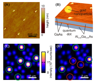
The quantum dots in our sample are lens-shaped GaAs inclusions of about 10 nm diameter and 5 nm height embedded in a AlGaAs barrier of larger band-gap. The two optically active dipole transitions of the neutral excitons show splittings of less than 90 eV which can be ascribed to slight dot-shape anisotropies plumhof:10 . With a ground state exciton emission wavelength around 760 nm, these quantum dots are well suited for Si-based single photon detectors. The quantum dots were grown using molecular beam epitaxy. In a first step a template of nanoholes was created by arsenic debt epitaxy on a GaAs (100) substrate gonzalez:2009 . During further growth steps the sample topography is preserved and the holes are visible by atomic force microscopy on the sample surface (1a). The quantum dots are formed by first depositing the AlGaAs barrier material followed by a layer of GaAs. During this growth step, GaAs accumulates in the holes and forms the quantum dots, while outside the holes only a thin GaAs wetting layer remains plumhof:10 ; wang:2009 . A detailed description of sample growth is given in the supplementary material. The quantum dots are located 10 nm beneath the sample surface. The shallow depth of the emitters enables near-field coupling with plasmonic structures placed on the sample surface. Here we use gold nanoparticles positioned above the quantum dots to act as optical antennas. A schematic of the studied structure is shown in 1b.
The quantum dots can be excited resonantly, i.e., by absorption of a photon by the quantum dot, or non-resonantly by carriers that are created outside the dot and diffuse into it. Here we excite the quantum dot non-resonantly by creating electrons and holes in the barrier and wetting layer using an optical parametric oscillator. The oscillator produces 400 fs pulses with a photon energy that can be tuned between 1.8 and 2.4 eV. The photoluminescence is collected in a home-built low-temperature confocal laser scanning microscope. The spatial resolution is limited by the objective’s numerical aperture (NA = 0.7) to approximately 600 nm. The photoluminescence can be spectrally analyzed using a spectrometer equipped with a charge coupled device camera. The spectral resolution of the setup is around 100 eV. For time-resolved measurements we employ time-correlated single photon counting with a temporal resolution of approximately 30 ps, which is much shorter than the measured exciton decay time of about 350 ps. All the optical measurements were performed at a temperature of 10 K.
As optical antennas we use spherical gold nanoparticles with a diameter of 90 nm as specified by the manufacturer (Nanopartz Inc.). The nanoparticles were deposited on the sample surface by drop casting from an aqueous solution. The sample had been patterned with markers so that the same area can be studied with AFM and optical microscopy. An AFM was used to identify regions of the sample with a low concentration of gold particles. Ten of the nanoparticles were moved on top of nearby quantum dots using the AFM tip. The optical properties of nanoantennas were characterized by recording the scattering spectrum of single antennas using dark-field microspectroscopy schultz:2000 ; sonnichsen:2002 . Details of the dark-field spectroscopy are given in the supplementary material.
1c shows a raster-scanned photoluminescence image of the region of the sample containing antenna-coupled emitters. For each bright, diffraction-limited spot in the luminescence image one can find a corresponding surface depression in an AFM image of the same area of the sample. The majority of the quantum dots are comparable in brightness. The emitters decorated with a gold nanoparticle, however, appear markedly brighter as seen in 1c. To exclude a coincidence, we removed the particle from three quantum dots (marked by red circles in 1d) after characterizing their optical properties. The photoluminescence of these three quantum dots changed to approximately the ensemble average value.
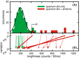
To quantify the influence of the nanoparticle on the emission properties of the quantum dots, we analyzed the photoluminescence of 228 emitters by fitting a two-dimensional Gaussian function to each emission spot in the luminescence image. The thus obtained brightness distribution is shown in 2. The center of the distribution was determined as 194 counts/30 ms (6470 counts/s) by fitting a Gaussian function to the histogram. The brightness of the 10 emitters coupled to a nanoantenna was determined in a similar fashion. We observe an increase in the photoluminescence intensity of up to a factor of 6 compared to the ensemble average. All our antenna-coupled quantum dots have a brightness that is greater than the ensemble average value. One advantage of our approach is the possibility to compare the properties of an emitter-antenna complex directly with those of the same single emitter without the antenna. Here we did this by removing the gold nanoparticle from the quantum dot for the three dots encircled in red in 1d. The change in the photoluminescence intensity is shown in 2b. Both the reference quantum dots and the unmodified emitter-antenna complexes remain at a similar brightness, as expected. The brightness of the three emitters from which the antennas were removed decreased to a value well within the ensemble distribution. For these quantum dots we deduce photoluminescence enhancement factors of 3.5, 3.7, and 6.1 when compared to their emission without antenna. The spread in the enhancement can be explained by a variation of the relative position of the antennas with respect to the quantum dots.
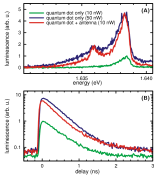
To determine the origin of the enhancement in photoluminescence intensity let us compare the emission spectra of the quantum dots with and without antenna as shown in 3a. We remark that the photoluminescence spectrum displayed in 3a for the quantum dot coupled to the antenna was shifted in energy by 1.4 meV to compensate for spectral shifts most likely due to surface charges in the vicinity of the quantum dot. At 10 nW excitation power the emission spectrum of the quantum dot without antenna is dominated by the exciton transition (3a). At 50 nW excitation power the exciton line starts to saturate and a second emission line appears. Compatible with previous reports on GaAs/AlGaAs dots wang:2009 , we identify this as one of the trions, i.e., charged exciton, transition from its super-linear excitation power dependence and its lifetime. The antenna-enhanced quantum dots show already at 10 nW excitation power an emission spectrum that resembles that of the unenhanced emitter at higher excitation power (3a). From this we conclude that the emitter in the quantum dot-nanoparticle complex experiences an about 5 times higher excitation power density due to the gold particle. The field enhancement around the plasmonic nanoparticle locally increases the probability that an electron-hole pair is created. The photoluminescence enhancement as determined from luminescence images is 6.1 for this emitter. This is in good agreement with the ratio of the excitation powers for which the emission spectra of the quantum dot with and without antenna is similar. Also for the other emitters the agreement between the enhancement values determined with the two methods was good. We can thus attribute the brightness enhancement predominantly to an increase of the excitation rate. This is also supported by measurements of spectrally integrated luminescence decay. In 3b we show the luminescence decay traces corresponding to the spectra displayed in 3a for 10 nW excitation power and for 50nW with and without antenna, respectively. We observe no significant changes in the decay dynamics due to the antenna.
We note that the emission lines of the antenna-quantum dot complexes appear slightly narrower than the emission of the same dots without antenna at comparable emission intensity. In the usual far-field excitation scheme carriers are generated in a larger volume than in the presence of the antenna. This leads to fluctuating charges, broadening the dot’s emission by spectral diffusion.
To further elucidate the effect of the plasmonic antenna on the optical properties of the quantum dots in our structure we have studied the influence of the excitation wavelength on the photoluminescence. For non-resonant excitation, the luminescence rate of the emitters depends on the carrier density in their vicinity and their diffusion into the quantum dot. Assuming a dipole transition, for low excitation power the carrier density is proportional to the local intensity of the electromagnetic field. The excitation rate of the quantum dots will thus be maximized when the excitation photon energy is tuned to the antenna resonance.
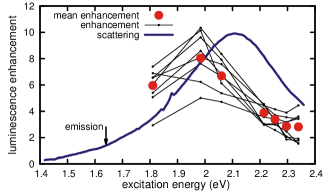
4 shows the photoluminescence enhancement of the quantum dots coupled to a nanoparticle antenna as a function of excitation energy for an average excitation power of about 50 nW. The enhancement was determined by comparing the brightness of the antenna-enhanced emitters to an ensemble of reference quantum dots that were not coupled to an antenna. We observe a peak in the measured photoluminescence enhancement at approximately 2.0 eV energy. At the plasmon resonance the electromagnetic field is enhanced close to the particle and the excitation rate of electron-hole pairs in the vicinity of the quantum dot is thus increased. The enhancement maximum occurs at a slightly lower energy than the plasmon resonance as seen from the scattering spectrum shown in 4. This is in agreement with the report of Bryant et al. Bryant:2008 that the near-field resonance occurs red-shifted of the far-field scattering resonance. The emission of the quantum dots is not modified (3b) as it occurs far off the antenna’s plasmon resonance.
In summary, we have introduced single epitaxial GaAs quantum dots as emitters for plasmonics by demonstrating the controlled enhancement of the excitation efficiency. Placing a gold nanoparticle in the vicinity of the emitter resulted in an increase in the photoluminescence intensity of about a factor of eight. In the near-field of the antenna close to the quantum dot more carriers are generated so that the excitation rate is increased. Our conclusion is supported by the observation that the decay dynamics of the emitters is unaltered by the coupling to the antenna. Varying the wavelength of the incident light clearly demonstrates that the photoluminescence enhancement originates from the plasmon resonance of the antenna.
Our scheme can be applied to more complex antennas and more than one emitter. For example, rod-like plasmon resonant metal particles can be positioned in the same way as here using AFM. Moreover, the topography of the quantum dots can be used to first determine their position and subsequently fabricate antenna structures by electron-beam lithography on top of them. The GaAs quantum dots provide a stable, solid-state source of photons that, when coupled to plasmonic nanostructures, forms an attractive system in which to study light-matter interactions and to use as a basis for nanophotonic applications.
We thank A. Vlandas for assistance with atomic force microscopy, L. Wang, F. Ding and B. Eichler for the growth and characterization of test samples, and the Deutsche Forschungsgemeinschaft DFG for funding (research unit FOR 730).
References
- (1) Chang, D. E.; Sørensen, A. S.; Hemmer, P. R.; Lukin, M. D. Phys. Rev. Lett. 2006, 97, 053002.
- (2) Akimov, A. V.; Mukherjee, A.; Yu, C. L.; Chang, D. E.; Zibrov, A. S.; Hemmer, P. R.; Park, H.; Lukin, M. D. Nature (London) 2007, 450, 402.
- (3) Fedutik, Y.; Temnov, V. V.; Schöps, O.; Woggon, U.; Artemyev, M. V. Phys. Rev. Lett. 2007, 99, 136802.
- (4) Shimizu, K. T.; Woo, W. K.; Fisher, B. R.; Eisler, H. J.; Bawendi, M. G. Phys. Rev. Lett. 2002, 89, 117401.
- (5) Liu, Y.; Blair, S. Opt. Lett. 2003, 28, 507.
- (6) Farahani, J. N.; Pohl, D. W.; Eisler, H.-J.; Hecht, B. Phys. Rev. Lett. 2005, 95, 017402.
- (7) Mertens, H.; Polman, A.Appl. Phys. Lett. 2006, 89, 211107.
- (8) Tam, F.; Goodrich, G. P.; Johnson, B. R.; Halas, N. J. Nano Lett. 2007, 7, 496.
- (9) Ringler, M.; Schwemer, A.; Wunderlich, M.; Nichtl, A.; Kürzinger, K.; Klar, T. A.; Feldmann, J. Phys. Rev. Lett. 2008, 100, 203002.
- (10) Bek, A.; Jansen, R.; Ringler, M.; Mayilo, S.; Klar, T. A.; Feldmann, J. Nano Lett. 2008, 8, 485.
- (11) Kinkhabwala, A.; Yu, Z.; Fan, S.; Avlasevich, Y.; Müllen, K.; Moerner, W. E. Nature Photonics 2009, 3, 654.
- (12) Schietinger, S.; Barth, M.; Aichele, T.; Benson, O. Nano Lett. 2009, 9, 1694.
- (13) Taminiau, T. H.; Stefani, F. D.; Segering, F. B.; van Hulst, N. F. Nature Photonics 2008, 2, 234.
- (14) Chang, D. E.; Sørensen, A. S.; Demler, E. A.; Lukin, M. D. Nature Phys. 2007, 3, 807.
- (15) Michler, P.; Kiraz, A.; Schoenfeld, W. V.; Petroff, P. M.; Zhang, L.; Hu, E.; Imamoǧlu, A. Science 2000, 290, 2282.
- (16) Plumhof, J. D.; Křápek, V.; Wang, L.; Schliwa, A.; Bimberg, D.; Rastelli, A.; Schmidt, O. G. Phys. Rev. B 2010, 81, 121309.
- (17) Alonso-González, P.; Martín-Sánchez, J.; González, Y.; Alén, B.; Fuster, D.; González, L. Crystal Growth and Design 2009, 9, 2525.
- (18) Wang, L.; Křápek, V.; Ding, F.; Horton, F.; Schliwa, A.; Bimberg, D.; Rastelli, A.; Schmidt, O. G. Phys. Rev. B 2009, 80, 085309.
- (19) Schultz, S.; Smith, D. R.; Mock, J. J.; Schultz, D. A. Proc. Natl. Acad. U.S.A. 2000, 97, 996.
- (20) Sönnichsen, C.; Franzl, T.; Wilk, T.; von Plessen, G.; Feldmann, J.; Wilson, O.; Mulvaney, P. Phys. Rev. Lett. 2002, 88, 077402.
- (21) Bryant, G. W.; de Abajo, F. G.; Aizpurua, J. Nano Lett. 2008, 8, 631.
I Supplementary Material
I.1 Growth of the quantum dots
The GaAs quantum dots are grown by molecular beam epitaxy. A low density ( cm-2) of self-assembled nanoholes approximately 10 nm deep and 100 nm wide were created by arsenic debt epitaxy in a GaAs (100) substrate [S1]. Deposition of 21 repeats of 0.4 monolayers Ga / 0.15 monolayers GaAs lead to droplets of excess gallium on the surface. A 5 minute interrupt under excess arsenic at a substrate temperature of 520 ∘C results in the formation of nanoholes surrounded by a raised GaAs ring due to the transfer of arsenic from the substrate to the gallium droplets [S2]. A 10 nm bottom Al0.45Ga0.55As barrier was then grown over the nanoholes, followed by a 2 nm GaAs layer, an 8 nm top Al0.45Ga0.55As barrier and a final 2 nm GaAs capping layer. The substrate temperature was then reduced from 520 ∘C to approximately 200 ∘C, and one monolayer of gallium was deposited to ensure a gallium terminated surface followed by cm-2 silicon to passivate the surface states [S3]. During the growth of the AlGaAs layers the shape of the nanoholes is well preserved. However, due to the greater migration length of gallium compared to aluminium, there is accumulation of gallium at the bottom of the nanohole during deposition of the GaAs layer leading to GaAs quantum dot formation [S4]. At the end of the growth, there is still a 2 nm deep depression in the sample surface marking the position of the quantum dot in the self-assembled nanohole. The elevated feature corresponds to the GaAs ring while the depression is at the position of the quantum dot.
I.2 Dark-field microspectroscopy
Dark-field scattering spectra of the gold nanoparticles were obtained using a home-built dark-field microspectroscopy setup. Light from a halogen lamp was used to illuminate the sample through a dark-field objective (Olympus MPlanFL N 100/0.90 BD). The sample was positioned using a piezoelectric positioning system. The light back-scattered by a nanoparticle was collected with the microscope objective and directed to a 500 mm focal length grating spectrometer equipped with a liquid nitrogen cooled charge coupled device camera. A reference spectrum was collected from an area on the sample without nanoparticles and subtracted from the scattering spectrum of the particle. Finally, to compensate for the wavelength dependent transmission of the optical train, the emission spectrum of the lamp, and the wavelength dependent sensitivity of the camera, a bright-field reflection spectrum of the sample from an area without nanoparticles was measured. This spectrum was used to normalize the dark-field spectra to obtain the scattering spectra of the nanoparticles.
I.3 References
[S1] Alonso-González, P.; Martín-Sánchez, J.; González, Y.; Alén, B.; Fuster, D.; González, L. Crystal Growth & Design 2009, 9, 2525.
[S2] Heyn, Ch.; Stemmann, A.; Hansen, W. Appl. Phys. Lett. 2009, 95, 173110.
[S3] Hasegawa, H.; Akazawa, M. Appl. Surf. Sci. 2008, 255, 628.
[S4] Rastelli, A.; Stufler, S.; Schliwa, A.; Songmuang, R.; Manzano, C.; Costantini, G.; Kern, K.; Zrenner, A.; Bimberg, D.; Schmidt, O. G. Phys. Rev. Lett. 2004, 92, 166104.