Optically and electrically controlled polariton spin transistor
Abstract
We propose two schemes of a novel spin-optronic device, optical analog of Datta and Das spin transistor for the electrons. The role of ferromagnetic contacts is played by one-dimensional polariton channels with strong TE-TM splitting. A symmetric 2D trap plays a role of the non-magnetic active region. The rotation of the polarization of the pulse in this region can be achieved either due to its interaction with a spatially confined polariton condensate created resonantly by a circular polarized laser, either due to the splitting between the two linear polarizations of the excitons, controlled electrically by use of metallic gate.
pacs:
71.36.+c, 42.65.Pc, 42.55.SaA number of important phenomena in condensed matter physics are connected with the spin of elementary excitations of different kinds: electrons, holes, excitons, or exciton-polaritons. The possibility to manipulate and control the spins of individual particles opens a way to the implementation of spin degree of freedom in nano- electronic devices of the new generation: spintronic devices (if spin of electrons or holes is used Žutić et al. (2004)) and spinoptronic devices (if spin of excitons or exciton polaritons is used Shelykh et al. (2010)).
The first spintronic device was proposed in early 90ies in the pioneer work of S. Datta and B. Das Datta and Das (1990). It consists of two ferromagnetic electrodes with collinear magnetizations, separated by a non-magnetic semiconductor region with Rashba Spin-Orbit Interaction (SOI). The Rashba Hamiltonian can be interpreted in terms of an effective magnetic field in the plane of a QW, perpendicular to the kinetic momentum of the carriers and charachterized by the Rashba parameter which can be efficiently tuned by varying the gate voltage applied to the top gate metallic electrode covering the non-magnetic region Nitta et al. (1997); Heida et al. (1998); Engels et al. (1997). When the spin-polarized carriers enter the non-magnetic region, this effective field provokes the rotation of their spins. Depending on the rotation angle , the transmitted current reveals periodic oscillations with minima and maxima corresponding to angles and , respectively. Due to the problems of spin injection and decoherence Datta and Das device remained for a long time the a purely theoretical concept, and it has been realized experimentally only recently Koo et al. (2009).
On the other hand, in the domain of mesoscopic optics it was proposed to use exciton-polaritons for creation of spinoptronic devices representing optical analogs of spintronic devices. Exciton-polaritons (or cavity polaritons) are the elementary excitations of semiconductor microcavities in the strong coupling regime. Being composite particles consisting of bright heavy-hole excitons and photons, polaritons have two allowed spin projections on the structure growth axis (), corresponding to the right and left circular polarisations of the counterpart photons. Thus, from the formal point of view, the spin structure of cavity polaritons is similar to the spin structure of electrons (both are two-level systems), and their theoretical description can be carried out along similar lines. It should be noted, however, that the statistics of elementary excitations is different in two kinds of systems: fermionic in the case of spintronics, bosonic in the case of spin-optronics. Also, it appears that the account of many-body interactions is of far greater importance for spinoptronic devices with respect to the spintronic ones Shelykh et al. (2010).
It was recently proposed that in the domain of spinoptronics the problems of spin injection and decoherence can very probably be resolved: the coherent length for polaritons is orders of magnitude longer than that of electrons Langbein et al. (2007) and the spin of the injected polaritons can be easily tuned by simple change of polarization of the exciting laser. The first spinoptronic device, namely polarization controlled optical gate, was recently realized experimentally Leyder et al. (2007), and theoretical schemes of several others were theoretically proposed. Among the latter one should mention two proposals for optical analog of the spin transistor: polariton Berry phase interferometer Shelykh et al. (2009) and polariton Datta and Das device Johne et al. (2010). Both of them require strong magnetic fields for their operation, which complicates their experimental realization and technological implementations. In the present letter we propose two new schemes of the polariton analog of Datta and Das device, which do not require any magnetic field and where the tuning of the transmitted polariton ”current” can be achieved by purely optical or electrical methods.
The geometries of the two schemes are shown at Fig. 1 (a). In both of them, the role of ferromagnetic contacts is played by 1D polariton channels (polariton waveguides), where due to the strong TE-TM splitting which is inversly proportional to the waveguide dimension Dasbach et al. (2005) and plays a role of magnetic field in ferromagnetic electrodes there is a region of the energies, where the mode with TM linear polarization can propagate. In realistic channels the value of the splitting can be as high as 1-2 meV for a waveguide of m width Kuther et al. (1998). Technologically, polariton waveguiding can be achieved by etching Dasbach et al. (2005), variation of the cavity thickness Kaitouni et al. (2006), applying stress Balili et al. (2006), or putting metals on the surface of the cavity Lai et al. (2007); Kaliteevskii et al. (2009). The 1D channels are connected to a symmetric 2D trap (active region), where the TE-TM splitting is absent. This trap plays a role of the nonmagnetic region. An effective magnetic field acting on the pseudospin of the pulse of the linear polarized polaritons in the active region can be created by two alternative ways.
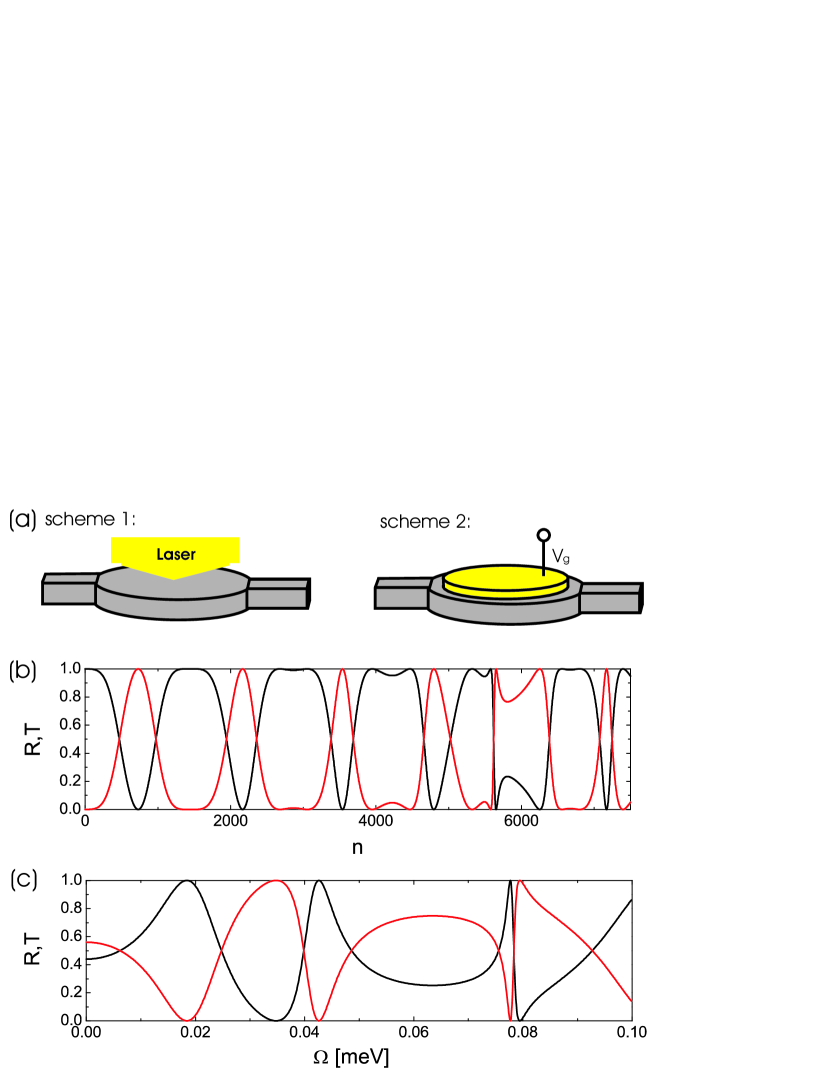
Scheme 1. For optically controlled transistor, one creates a circular polarized polariton condensate in the region of the trap by a resonant cw pump. After entering this active region, the polaritons from the pulse start interacting with polaritons of the condensate. These interactions are strongly spin-anisotropic: the interaction of polaritons in the triplet configuration (parallel spin projections on the structure growth axis) is much stronger than that of polaritons in the singlet configuration (antiparallel spin projections) Renucci et al. (2005). This leads to a mixing of linearly polarised polariton states, manifesting itself in the appearance of a z-directed effective magnetic field acting on polariton pseudospin. In the geometry we consider, this will lead to the rotation of the pseudospin of the pulse along the z-axis. The rotation angle can be estimated as
| (1) |
where L is the length of the active region, is the effective mass of the polaritons, is their in-plane wavenumber, and is a pump-induced splitting in circular polarizations in the active region with being the constants characterizing the interaction of the polaritons in the singlet and triplet configurations Glazov et al. (2009), being the 2D density of circular polarized polariton condensate in a trap. In complete analogy with the electronic Datta and Das transistor, due to the strong TE-TM splitting in the leads one expects periodic dependence of the polariton current on . As depends on the condensate density , the transmitted polariton current can be modulated by tuning the intensity of the circular polarized laser pump.
Scheme 2. The rotation of the polarization of the pulse in the active region can be also achieved by purely electrostatic method via the application of a metallic gate electrode. Variation of the gate voltage results in the changing of the asymmetry of the QWs in the direction of the structure growth axis , which leads to the splitting in the energies of the excitonic (and polaritonic) states with linear polarizations parallel to main crystalline axes Aleiner and Ivchenko (1992); Malpuech et al. (2006) and appearance of the corresponding effective in-plane magnetic field. If there is an angle of between crystalline axes and polariton waveguides, the effective magnetic fields in the waveguides and in the active region are perpendicular, and thus the pseudospin of the linear polarized pulse entering the active region will undergo the rotation by the angle given again by Eq.1, the only difference being that now is the splitting in the active region induced by the top gate, dependent on . The tuning of the gate voltage will thus result in the periodic modulation of the outgoing polariton current.
For quantitative description of the polariton transport in the system considered, we first use a simplified model, treating the polariton waveguides and the active region as quasi-1D. The transmission and reflection amplitudes in this case can be found from the solution of the one- dimensional scattering problem with the following Hamiltonian written in a basis of circular polarizations
| (5) |
where we divide the system into three regions: (1) (ingoing waveguide), (2) (active region) and (3) (outgoing waveguide). The axis x was chosen to be parallel to the direction of the leads, in the intermediate region one should use the term for the scheme 1 and for the scheme 2 with denote Pauli matrices. - polariton effective mass, - longitudinal- transverse splitting in the leads, - effective magnetic field in the active region 2, the energy offset between polaritons in the waveguides and active region appearing from the confinement effects. The solutions of the stationary Schrodinger equation with a wavefunction being a spinor and Hamiltonian 5 in all three regions read:
| (6) | |||||
| (8) |
where and are the reflection and transmission amplitudes, , with being the energy of the polaritons counted from the bottom of the lowest TM mode in the waveguides. are the complex amplitudes of forward (backward) running waves in the active region with different polarisations and wavevectors . The vectors read for scheme 1
| (9) |
and
| (10) |
for scheme 2. The reflection and transmission amplitudes can be then found using the standard conditions of continuity of the wavefunctions and the current at the interfaces between the regions 1 and 2 and 2 and 3.
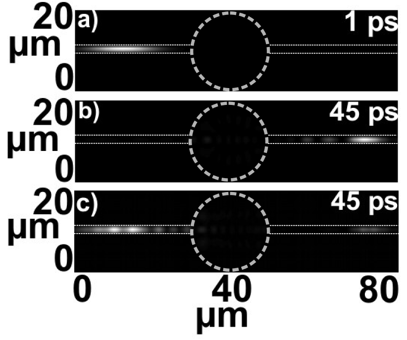
Fig.1 (b) shows the dependence of the transmission coefficient and reflection coefficient on the density of the optically pumped condensate for scheme 1 and Fig.1 (c) on for scheme 2. The calculation is performed taking into account realistic parameters of a GaAs microcavity. One sees that in both cases there is an oscillating dependence of the outgoing polariton current on the control parameter, and thus the system pefectly matches the definition of a polariton spin transistor.
We have also performed a realistic numerical simulation of the device operation. We describe the propagation of a linear polarized pulse through the system with the use of coupled 2D spinor Gross-Pitaevskii equation for excitons and Schroedinger equation for photons Shelykh et al. (2006), which for the case of the electrically controlled transistor (scheme 2) read
| (11) | |||
| (12) | |||
where , with correspond to the excitonic and photonic fields written in basis of circular polarizations, and are effective masses of 2D excitons and photons respectively, and are their lifetimes, is the Rabi splitting, are two constants characterizing polariton- polariton interactions, and are profiles of the in- plane confinement potential for the photons, splitting between the linear polarizations of the photonic mode and effective magnetic field in the active region respectively. The waveguides have a thickness of m, and the radius of the active region is m. In this region the pulse is rotated by an effective magnetic field induced by the voltage applied to the gate electrode. The transition between the waveguides and the active region has to be sufficiently smooth in order to minimize the diffraction effects, which would decrease the transmission coefficient in the case. In our calculations we have considered photon lifetime 16 ps, exciton lifetime 100 ps, LT splitting in the leads 4 meV, Rabi splitting =8 meV.
Figure 2 shows the results of the numerical simulations - the calculated real-space images of the photon emission. Panel (a) shows the gaussian pulse ( m-1) created by an external laser. The pulse should be sufficiently large in real space, in order to avoid the dispersion effects. The pulse propagates through the system quite rapidly, and after 45 ps leaves the active region through the waveguide. Panel (b) shows the case (100% transmission) and panel (c) corresponds to meV, which reduces the transmission to approximately 20%. The potential profile is indicated by the dashed lines.
Due to the rapid propagation of the pulse in the considered device, its operation time will be limited by the time needed to tune the values of the effective magnetic field in the active region. For the electrically controlled transistor this time is determined by the characteristic time of the tuning of the gate voltage and thus should be of the same order of magnitude as characteristic operation time for a standard Datta and Das transistor for the electrons. For optically controlled transistor (scheme 1), this time is determined by the time of the formation of stationary polariton distribution under the effect of the coherent circular polarized pump. The latter can be simply estimated by the longest characteristic time in the system, which is the exciton lifetime of the order of 100 ps in GaAs structures. This corresponds to an operation frequency of 10 GHz. Note also, that the recent proposal of engineering of the polariton confinement using a deposition of the metallic mesas of needed geometry Kaliteevskii et al. (2009) allows creation of polariton integrated circuits consisting from several transistors of the considered geometry.
In conclusion, we proposed two novel schemes of a polaritonic analogue of Datta and Das spin transistor, which does not need magnetic fields for operation. The proposed geometry allows to solve the problems of decoherence and inefficient spin injection which were blocking the experimental implementation of Datta and Das spin transistor for electrons. The device transmissivity is easily and quickly controlled tuning the intensity of the pumping laser or simply the gate voltage.
I.A.S. acknowledges the support from RANNIS ”Center of excellence in polaritonics” and FP7 IRSES project ”SPINMET”.
References
- Žutić et al. (2004) For review on spintronics, see e.g. I. Žutić, J. Fabian, and S. Das Sarma, Rev. Mod. Phys., 76, 323 (2004).
- Shelykh et al. (2010) For review on spin-optronics, see I. A. Shelykh, A. V. Kavokin, Y. G. Rubo, T. C. H. Liew, and G. Malpuech, Semiconductor Science and Technology, 25, 013001 (2010).
- Datta and Das (1990) S. Datta and B. Das, Applied Physics Letters, 56, 665 (1990).
- Nitta et al. (1997) J. Nitta, T. Akazaki, H. Takayanagi, and T. Enoki, Phys. Rev. Lett., 78, 1335 (1997).
- Heida et al. (1998) J. P. Heida, B. J. van Wees, J. J. Kuipers, T. M. Klapwijk, and G. Borghs, Phys. Rev. B, 57, 11911 (1998).
- Engels et al. (1997) G. Engels, J. Lange, T. Schäpers, and H. Lüth, Phys. Rev. B, 55, R1958 (1997).
- Koo et al. (2009) H. Koo, J. Kwon, J. Eom, J. Chang, S. Han, and M. Johnson, Science, 325, 1515 (2009).
- Langbein et al. (2007) W. Langbein, I. Shelykh, D. Solnyshkov, G. Malpuech, Y. Rubo, and A. Kavokin, Phys. Rev. B, 75, 075323 (2007).
- Leyder et al. (2007) C. Leyder, T. C. H. Liew, A. V. Kavokin, I. A. Shelykh, M. Romanelli, J. P. Karr, E. Giacobino, and A. Bramati, Phys. Rev. Lett., 99, 196402 (2007).
- Shelykh et al. (2009) I. A. Shelykh, G. Pavlovic, D. D. Solnyshkov, and G. Malpuech, Phys. Rev. Lett., 102, 046407 (2009).
- Johne et al. (2010) R. Johne, I. A. Shelykh, D. D. Solnyshkov, and G. Malpuech, Phys. Rev. B, 81, 125327 (2010).
- Dasbach et al. (2005) G. Dasbach, C. Diederichs, J. Tignon, C. Ciuti, P. Roussignol, C. Delalande, M. Bayer, and A. Forchel, Phys. Rev. B, 71, 161308(R) (2005).
- Kuther et al. (1998) A. Kuther, M. Bayer, T. Gutbrod, A. Forchel, P. A. Knipp, T. L. Reinecke, and R. Werner, Phys. Rev. B, 58, 15744 (1998).
- Kaitouni et al. (2006) R. I. Kaitouni, O. El Daif, A. Baas, M. Richard, T. Paraiso, P. Lugan, T. Guillet, F. Morier-Genoud, J. D. Ganière, J. L. Staehli, V. Savona, and B. Deveaud, Phys. Rev. B, 74, 155311 (2006).
- Balili et al. (2006) R. B. Balili, D. W. Snoke, L. Pfeiffer, and K. West, Applied Physics Letters, 88, 031110 (2006).
- Lai et al. (2007) C. Lai, N. Kim, S. Utsunomiya, G. Roumpos, H. Deng, M. Fraser, T. Byrnes, P. Recher, N. Kumada, T. Fujisawa, et al., Nature, 450, 529 (2007).
- Kaliteevskii et al. (2009) M. Kaliteevskii, S. Brand, R. Abram, I. Iorsh, A. Kavokin, and I. Shelykh, Applied Physics Letters, 95, 251108 (2009).
- Renucci et al. (2005) P. Renucci, T. Amand, X. Marie, P. Senellart, J. Bloch, B. Sermage, and K. V. Kavokin, Phys. Rev. B, 72, 075317 (2005).
- Glazov et al. (2009) Usually . For detailed description of spin-anisotropic polariton-polariton interaction see M. M. Glazov, H. Ouerdane, L. Pilozzi, G. Malpuech, A. V. Kavokin, and A. D’Andrea, Phys. Rev. B, 80, 155306 (2009). and T. Ostatnicky, D. Read, and A. V. Kavokin, Phys. Rev. B, 80, 115328 (2009).
- Aleiner and Ivchenko (1992) I. Aleiner and E. Ivchenko, JETP Lett, 55, 692 (1992).
- Malpuech et al. (2006) G. Malpuech, M. Glazov, I. Shelykh, P. Bigenwald, and K. Kavokin, Applied Physics Letters, 88, 111118 (2006).
- Shelykh et al. (2006) I. A. Shelykh, Y. G. Rubo, G. Malpuech, D. D. Solnyshkov, and A. Kavokin, Phys. Rev. Lett., 97, 066402 (2006).