Drain current modulation in a nanoscale field-effect-transistor channel by single dopant implantation
Abstract
We demonstrate single dopant implantation into the channel of a silicon nanoscale metal-oxide-semiconductor field-effect-transistor. This is achieved by monitoring the drain current modulation during ion irradiation. Deterministic doping is crucial for overcoming dopant number variability in present nanoscale devices and for exploiting single atom degrees of freedom. The two main ion stopping processes that induce drain current modulation are examined. We employ 500 keV He ions, in which electronic stopping is dominant, leading to discrete increases in drain current and 14 keV P dopants for which nuclear stopping is dominant leading to discrete decreases in drain current.
1
Classical metal-oxide-semiconductor field-effect-transistors (MOSFETs) fabricated by industrial methods are now sufficiently small that random variations in the number and placement of dopants results in inconsistent behaviour. This is already a major issue in the microelectronics industry for devices operating at room temperature.ITRS:2007wt Further, the Bohr radius of a donor electron is now a significant fraction of the device size resulting in the possibility of quantum mechanical dependent functionalities as observed with adventitiously doped devices at 4 K.LANSBERGEN:2008kx ; Pierre:2010uq ; klein:043107 Emerging deterministic doping technologies aim to mitigate statistical fluctuations in the doping of these devices while also providing significant potential for solid-state quantum computers.Kane:1998wj ; PhysRevA.62.012306 ; PhysRevB.67.121301 ; PhysRevB.74.045311
Low energy single dopant implantation into micronscale devices has been reported.Jamieson:2005aa ; batra:193502 Further, time-resolved control and transfer of a single electron between two deterministically implanted P atoms has been demonstrated.Andresen:2007kx Deterministic doping schemes which employ ion implantation are based on ion impact signals from electron-hole pairs,Jamieson:2005aa ; seamons:043124 secondary electronsShinada:2005zt ; persaud:2798 ; Persaud:2004df or modulation of the drain current, .weis:2596 ; batra:193502 ; shinada For the latter, discrete downward steps in have been observed with low energy Si implantation into a micronscale SOI wire.shinada However, for micronscale MOSFETs, other reports show discrete upward steps.weis:2596 ; batra:193502 By an appropriate choice of ion and implant energy we can selectively induce discrete upward or downward steps in to elucidate the mechanisms involved in these opposing responses in nanoscale MOSFETs. The full potential of new single-atom functionalities requires nanoscale devices. For example, multi-gate silicon-on-insulator (SOI) transistors are promising architectures.Tettamanzi:2010kl
Here, we examine modulation in nanoscale SOI MOSFETs from the passage through the channel of 500 keV He+ ions for which electronic stopping is the dominant mechanism for dissipation of the kinetic energy. We contrast this with the modulation induced by 14 keV P+ dopants which mainly stop in the channel and for which nuclear stopping is dominant. In the latter case this modulation is the deterministic signal where precision placement is optimised by using a specialised gate structure which also acts as a surface mask.
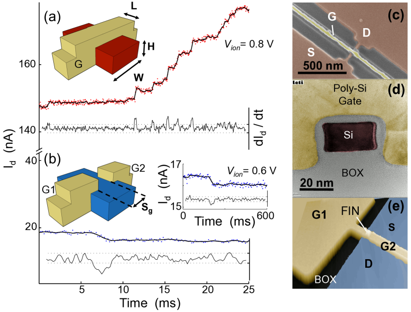
We fabricated finFETs with SOI consisting of 20 nm of Si on a 145 nm thick buried oxide (BOX). Images of the devices are shown in Figs. 1 (c)-(e). The channel had a 5 nm SiO2 gate oxide.pierre:242107 The nominal channel dimensions are listed in Table 1. The SiO2/Si interface is expected to have an interface state density in the mid- as measured by deep level transient spectroscopy. The gates were poly-Si and the source-drain contacts were As doped by ion implantation to a concentration of . Two MOSFET types were considered and are shown schematically in the inset of Fig. 1 (a) and (b). The first was a single gate MOSFET with full back-end processing that incorporated a surface passivation layer and was used for the He implantation experiments. The second type was a double gated MOSFET with a spacing between the two gates of nm. Si3N4 was formed around each gate leaving a space through which the channel was exposed to the ion beam.Pierre:2010uq
The MP2 beam-lineJamieson1997706 and a Colutron implanterJamieson:2005aa were used to irradiate the devices with 500 keV He+ and 14 keV P+, respectively. The source, drain and gate were bonded into a chip carrier with electrostatic discharge protection. The He+ beam was focused to produce a sharp horizontal line () that was scanned across the device and had a beam flux of . The P+ beam was directed through a stationary 600 diameter aperture at an average flux of . During implantation, was monitored at a gate voltage of which is shown for each device in Table 1. was chosen so that any shift in threshold voltage could be detected with the associated change in . The IV characteristics of all devices were measured before and a day after the irradiation using standard electronics (Keithley 487).
Figures 1 (a) and (b) show the variation of during He+ and P+ irradiations, respectively. Discrete steps in are observed in both cases and represented by peaks in the plot. For the He irradiated device there is some variation in the peak height. This can be understood from our PADRE941 device simulations (not shown) which suggest that the threshold voltage shift is most sensitive where the current density is high. An ion strike where the current density is low will have a smaller effect and an ion strike in the source or drain will have a negligible effect. Generally, the step heights become smaller as irradiation continues signifying that the IV curve is shifting to a point where does not vary significantly around . For the irradiation with P+ two discrete steps in are observed (Fig. 1 (b)). The second step is shown in the top right inset on a different scale. The time constant of this second step is much larger than the first and its height is also much smaller, most likely as a consequence of the transformation of a significant volume of the channel as a result of the previous ion strike. After irradiation, the devices remained robust and there was no observable change in gate leakage current.
Table 1 shows the estimated fluence calculated from the measured beam flux and the implant duration. The total exposure is the number of ions that would be implanted given this fluence and the device dimensions. The counted He+ impact signals are reasonably consistent with this estimate. For P+, the estimate does not take into account the reduced size of the exposed channel area caused by the Si3N4, hence the larger discrepancy. was found to step up with He+ implantation and down with P+. After the beam was no longer incident on , began to decrease over a longer time scale. This is indicative of the recombination of positive trapped oxide chargetrombetta:2512 and was not observed for P+ implanted devices.
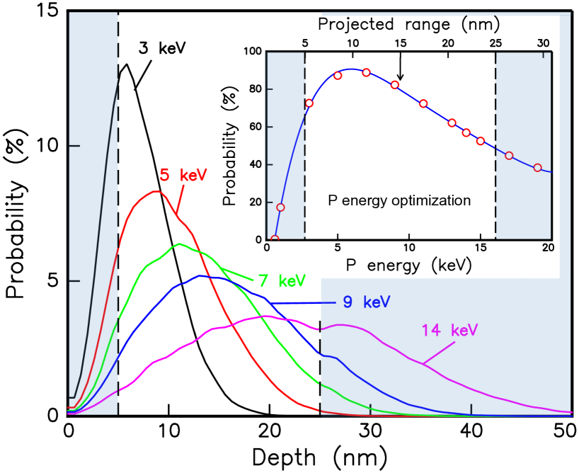
Monte Carlo SRIMsrim simulations of P+ implants into a simplified nanoscale SOI structure are shown in Fig. 2. While we demonstrate that a discrete number of ions can be implanted, they are subject to random statistical processes that cause straggle in the ion range. For these devices, a 5.9 keV P+ is optimimum for donor placement in the channel with a probability of 90%. We have used 14 keV for direct comparison with earlier work.Tan:2009uq This results in a 57% chance of the P+ stopping within the channel. SRIM simulations further show that the concentration of vacancies created by 14 keV P+ is an order of magnitude greater than 500 keV He in the channel of the MOSFET. Conversely, the He+ causes about twice as many ionisations than the P+. This illustrates that the mechanisms by which is modified depends greatly on the type and energy of implanted ion. Ionisation can result in trapped positive charge in the BOX.dekeersmaecker:532 In this work, it is likely that the dominant modulation is either caused by ionisations in the BOX for He+ and Frenkel pairs created in the channel region for P+.
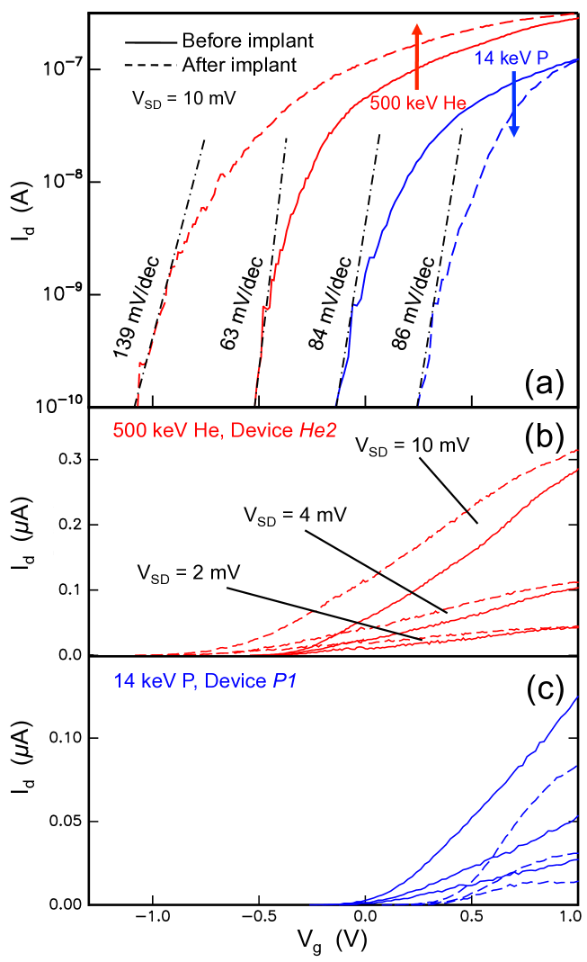
Figure 3 shows the IV curves for devices and before and one day after the implants. The He+ and P+ implantation induced defects modify the IV curves in different ways. Similar results are found for . The trapped oxide charge created in the BOX by the He implants can result in an inversion layer formed along the Si/BOX interface which causes interface coupling effects.Cristoleveanu:2004uq ; Eminente2007239 ; Daug2004535 This results in the observed negative shift. The charge density was estimated using analytical expressions of the subthreshold at midgap to be for both and .mcwhorter:133 In addition to a shift, there is a noticeable stretch-out, the extent of which is indicated by the subthreshold swing, in Fig. 3 (a). We find the associated effective change in interface trap density is and for devices and , respectively.
The P+ implantation caused quite different behaviour as seen in Fig. 3(c). A positive shift is observed suggesting that the interface states are negatively charged as is the case for n-type MOSFETs.90114 This shift corresponds to a charge density of . A decrease in is also observed (Fig. 3(b)) suggesting an increase in series resistance consistent with the introduction of Frenkel pairs in the channel.
In conclusion, the implantation of single P+ ions into a nanoscale SOI MOSFET was demonstrated. was found to depend on the stopping mechanisms and where in the substrate the ion energy was deposited. Electronic stopping resulted in trapped charge in the BOX causing a threshold voltage shift. Conversely, the detection of low energy implanted dopants required for deterministic doping relies on a series resistance increase caused by the introduction of Frenkel pairs into the channel.
The authors acknowledge nancial support from the EC FP7 FET-proactive NanoICT projects MOLOC (215750) and AFSiD (214989) and the Dutch Fundamenteel Onderzoek der Materie FOM.
References
- (1) “International technology roadmap for semiconductors,” (2007)
- (2) G. Lansbergen, R. Rahman, C. J. Wellard, I. Woo, J. Caro, N. Collaert, S. Biesemans, G. Klimeck, L. C. L. Hollenberg, and S. Rogge, Nat. Phys. 41, 656 (2008)
- (3) M. Pierre, R. Wacquez, X. Jehl, M. Sanquer, M. Vinet, and O. Cueto, Nat. Nanotechnol. 5, 133 (2010)
- (4) M. Klein, J. A. Mol, J. Verduijn, G. P. Lansbergen, S. Rogge, R. D. Levine, and F. Remacle, Appl. Phys. Lett. 96, 043107 (2010)
- (5) B. E. Kane, Nature 393 (1998)
- (6) R. Vrijen, E. Yablonovitch, K. Wang, H. W. Jiang, A. Balandin, V. Roychowdhury, T. Mor, and D. DiVincenzo, Phys. Rev. A 62, 012306 (2000)
- (7) M. Friesen, P. Rugheimer, D. E. Savage, M. G. Lagally, D. W. van der Weide, R. Joynt, and M. A. Eriksson, Phys. Rev. B 67, 121301 (2003)
- (8) L. C. L. Hollenberg, A. D. Greentree, A. G. Fowler, and C. J. Wellard, Phys. Rev. B 74, 045311 (2006)
- (9) D. N. Jamieson, C. Yang, T. Hopf, S. M. Hearne, C. I. Pakes, S. Prawer, M. Mitic, E. Gauja, S. E. Andresen, F. E. Hudson, A. S. Dzurak, and R. G. Clark, Appl. Phys. Lett. 86, 202101 (2005)
- (10) A. Batra, C. D. Weis, J. Reijonen, A. Persaud, T. Schenkel, S. Cabrini, C. C. Lo, and J. Bokor, Appl. Phys. Lett. 91, 193502 (2007)
- (11) S. E. S. Andresen, R. Brenner, C. J. Wellard, C. Yang, T. Hopf, C. C. Escott, R. G. Clark, A. S. Dzurak, D. N. Jamieson, and L. C. L. Hollenberg, Nano Letters 7, 2000 (2007)
- (12) J. A. Seamons, E. Bielejec, M. S. Carroll, and K. D. Childs, Appl. Phys. Lett. 93, 043124 (2008)
- (13) T. Shinada, S. Okamoto, T. Kobayashi, and I. Ohdomari, Nature 437, 1128 (2005)
- (14) A. Persaud, J. A. Liddle, T. Schenkel, J. Bokor, T. Ivanov, and I. W. Rangelow, J. Vac. Sci. Technol. B 23, 2798 (2005)
- (15) A. Persaud, S. J. Park, J. A. Liddle, I. W. Rangelow, J. Bokor, R. Keller, F. I. Allen, D. H. Schneider, and T. Schenkel, Quantum Inf. Process. 3, 233 (2004)
- (16) C. D. Weis, A. Schuh, A. Batra, A. Persaud, I. W. Rangelow, J. Bokor, C. C. Lo, S. Cabrini, E. Sideras-Haddad, G. D. Fuchs, R. Hanson, D. D. Awschalom, and T. Schenkel, J. Vac. Sci. Technol. B 26, 2596 (6 2008)
- (17) T. Shinada, T. Kurosawa, H. Nakayama, Y. Zhu, M. Hori, and I. Ohdomari, Nanotechnology 19, 345202 (2008)
- (18) G. C. Tettamanzi, A. Paul, G. P. Lansbergen, J. Verduijn, S. Lee, N. Collaert, S. Biesemans, G. Klimeck, and S. Rogge, IEEE Electron Device Letters 31, 150 (2010)
- (19) M. Pierre, R. Wacquez, B. Roche, X. Jehl, M. Sanquer, M. Vinet, E. Prati, M. Belli, and M. Fanciulli, Appl. Phys. Lett. 95, 242107 (2009)
- (20) D. N. Jamieson, Nucl. Inst. Meth. B 130, 706 (1997)
- (21) M. R. Pinto, K. Smith, M. A. Alam, S. Clark, X. Wang, G. Klimeck, and D. Vasileska, “Padre,” (2006), http://nanohub.org/resources/941
- (22) L. P. Trombetta, F. J. Feigl, and R. J. Zeto, J. Appl. Phys. 69, 2512 (1991)
- (23) J. F. Ziegler, J. P. Biersack, and U. Littmark, “The stopping and range of ions in solids (srim),” (1996), http://www.srim.org/
- (24) K. Y. Tan, K. W. Chan, M. Möttönen, A. Morello, C. Yang, J. v. Donkelaar, A. Alves, J.-M. Pirkkalainen, D. N. Jamieson, R. G. Clark, and A. S. Dzurak, Nano Letters 10, 11 (2010)
- (25) R. F. DeKeersmaecker and D. J. DiMaria, J. Appl. Phys. 51, 532 (1980)
- (26) S. Cristoleveanu and V. Ferlet-Cavrois, “Radiation effects and soft errors in integrated circuits and electronic devices,” (World Scientific, 2004) p. 181
- (27) S. Eminente, S. Cristoloveanu, R. Clerc, A. Ohata, and G. Ghibaudo, Solid State Electron. 51, 239 (2007)
- (28) F. Daugé, J. Pretet, S. Cristoloveanu, A. Vandooren, L. Mathew, J. Jomaah, and B. Y. Nguyen, Solid State Electron. 48, 535 (2004)
- (29) P. J. McWhorter and P. S. Winokur, Appl. Phys. Lett. 48, 133 (1986)
- (30) J. Srour and J. McGarrity, Proceedings of the IEEE 76, 1443 (1988)
| ID | Gate | Estimated | Total | Counted | ||
|---|---|---|---|---|---|---|
| type | (nm3) | fluence (cm-2) | exposurea | ions | (V) | |
| Double | b | P | 2 | 0.6 | ||
| Single | He | - | grounded | |||
| Single | He | 30 | 0.8 |
Upper limit of implanted ions into the device subject to Poisson statistics and experimental uncertainties.
The exposed space between the two gates on top of the channel, , was 50 nm wide. Si3N4 spacers decrease the exposed area further.