Density-functional studies of spin-orbit splitting in graphene on metals
Abstract
Spin-orbit splitting in graphene on Ni, Au, or Ag (111) substrates was examined on the basis of density-functional theory. Graphene grown on the three metals was found to have Rashba splitting of a few or several tens of meV. The strong splitting obtained on Au or Ag substrates was mainly ascribed to effective hybridization of graphene state with Au or Ag states, rather than charge transfer as previously proposed. Our work provides theoretical understandings of the metal-induced Rashba effect in graphene.
pacs:
73.22.-f, 71.70.Ej, 75.75.+a-
Graphene has attracted extensive attention in recent years due to its unique and remarkable electronic properties, such as gapless-semiconductor band, existence of pseudospin, and high electronic mobility at room temperature.geim ; nov ; zhang These features are highly desirable for the development of next-generation microelectronic and spintronic devices.nature ; sem Spin currents in graphene can be manipulated using various electronic tactics, in particular through exchange and spin-orbit (SO) interactions, which are now among the most active research topics in several realms.sem ; datta ; aws The intrinsic SO effect in pure graphene layers is nevertheless very weak, 0.10.37 meV in flat graphene sheet or carbon nanotube kane ; kue ; yao , insufficient for practical use due to the low nuclear charge of the carbon atom. It was hence very exciting when Dedkov et al reported an extraordinarily large Rashbara SO splitting (225 meV) for the states of epitaxial graphene layers on the Ni (111) substrate through their angle-resolved photoemission studies.ded It appears that the SO effect or hybridization in graphene can be tuned through effective electric field across the interface. However, this result was challenged by Rader et al rad who found that the sum of Rashba and exchange splitting in the graphene layer on either Ni (111) or Co(0001) is less 45 meV. They pointed out that the Rashba effect can be strongly enhanced by intercalation of one monolayer of Au between graphene and Ni (111). Clearly, to discriminate these contradictory experimental results and furthermore to understand the mechanism of substrate-induced SO splitting in graphene are crucial for the progress of graphene physics.
In this Letter, we report results of density-functional theory (DFT) kohn calculations for the electronic and magnetic properties of graphene on Ni, Au, or Ag (111) films. Interestingly, the Rashba splitting in graphene on Au and Ag can be significantly enhanced by strong hybridization of graphene state and metal state. The SO splitting is found to be almost independent of the charge transfer between graphene and its substrates, contradicting to effective electronic field model proposed in Ref.ded .
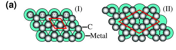
The electronic structures of graphene on metal (111) substrates, abbreviated as Gr/M (M = Ni, Au, and Ag), were calculated by using the VASP code at the level of local spin-density approximation (LSDA).lsda The projector-augmented wave (PAW) pseudopotentials were employed to describe the effect of core electrons. The equilibrium structures were obtained through structural relaxation until the Hellmann-Feynman forces were less than 0.05 eV/Å.prb The Gr/M systems were modeled by a periodic slab geometry, with a vacuum of at least 10 Å between two neighboring slabs. Each slab contains one graphene layer and N atomic layers of metal. Two adsorption configurations of graphene on the metal substrates were considered, as depicted in Fig.1(a). We found that configuration (I) is more stable for graphene on Ni (111), as it gives very small lattice mismatch (1%). For the same reason, configuration (II) is preferred for graphene on the larger Au and Ag (111) lattices kar ; gio . As a benchmark calculation for the SO effect, we first determined the SO splitting of the surface states (SS) of the pure Au (111) film near the Fermi level (EF, set as energy zero).nico Our result, 100 meV, agrees well with data in Ref.nico .
The band structures of Gr/Ni with N=13bertoni are given in Fig.1(b) and (c). The direction of Ni magnetization is set to be perpendicular to M. Despite the strong perturbation from the Ni (111) substrate, one can still easily trace several graphene bands in Fig.1(b), e.g., the graphene and states at -4 and -10 eV in the vicinity of the point. Compared to the band structures of pure graphene, these states are spin polarized, and shifted downward in energy by about 1.2 and 2.2 eV, respectively. Particularly, the feature conical points at near EF are destroyed in Fig.1(b), due to broken equivalence of A and B sublattices through the interaction with Ni. These results are in agreement with photoemission measurementsgash .
Now we zoom in to explore spin splitting and SO effect of the states of graphene along the - line, following the experimental workded ; rad ; gierz . To separate contributions from different factors, we studied cases either with or without the SO interaction. As illustrated in Fig.1(c), bands without the SO interaction are symmetric about the point and show an induced exchange splitting () of 30 meV on the magnetic Ni substrate. After considering the SO interaction, the energy splitting () contains two parts: exchange and SO (). The value of can be extracted through . The linear relationship of versus k in Fig.1(c) indicates that the SO interaction is indeed the Rashba type (, where is Rashba strength).ra ; rad The Rashba splitting obtained from our calculations is about 10 meV, in consistent with the experimental data in Ref. rad . In comparison with the SO splitting (0.37 meV) in curved graphenekue , the Ni-induced SO splitting in the graphene bands is relatively larger.
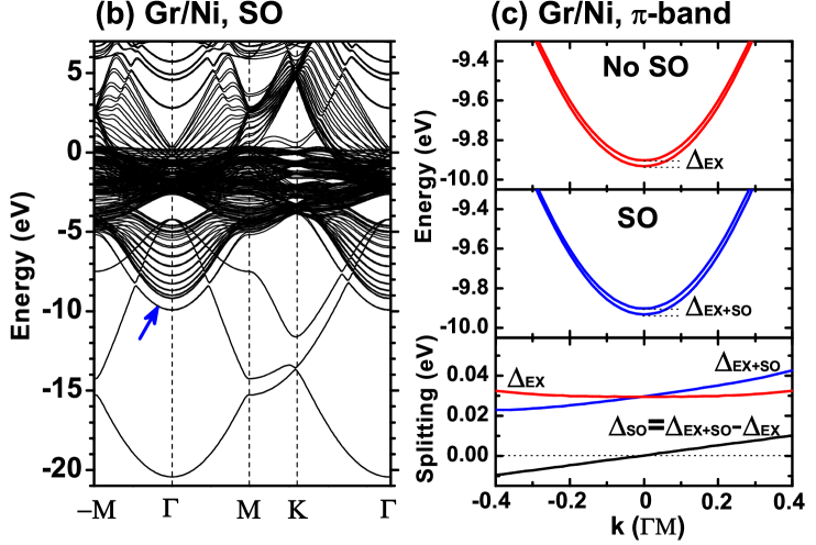
The energy bands of Gr/Au in the configuration (II), also with a fine lattice match, are given in Fig. 2, where different separation (d) between graphene and the Au substrate is considered. The bands of graphene are accompanied by a gold SS at = -7.3 eVliu , labeled as ’Au SS’ in Fig. 2(a). This Au SS is actually localized at the vacuum side of the Au slab and hence shows no change for different d in Fig. 2(a). The corresponding Au SSs at the graphene side move down quickly with the decrease of d due to the effect of graphene. At the equilibrium geometry (deq=3.3 Å), the SO splitting of graphene bands at 0.3 is about 21 meV, much larger than that on the Ni substrate. For Gr/Au in the configuration (II), the A and B sublattices experience the same environment again. Thus, the graphene layer almost restores its unique electronic structure: the Dirac cone near EF. Charge transfer between graphene and the metal and therefore the energy position of the Dirac cone can be adjusted through changing d.gio At the equilibrium separation, the Dirac point (Fig.2(b)) is very close to EF, indicating almost no charge transfer between graphene and Au. When the separation expands/shrinks, the Dirac point moves upward/downward, revealing net charge transfer between graphene and Au occurs. The SO splitting of graphene, however, reduces both ways, independent of the enhancement of effective electric field in the interface. This contradicts to the effective electric field model proposed in Refs.ded ; rad for the explanation of enhanced SO effect in the systems. The inset in Fig.2(b) shows the SO splitting of the Dirac point. Both the electron and hole bands show SO splitting of about 5 meV, close to the value (13 meV) given in recent experiment.va The splitting at the Dirac point is induced by the metal, as intrinsic SO interaction at this point was predicted to be zero. ya
| Ni (I) | Au (II) | Au (I) | Ag (II) | Ag (I) | |
|---|---|---|---|---|---|
| (N=13) | (N=9) | (N=12) | (N=9) | (N=12) | |
| Gr- state | 1.0 | 1.0 | 1.0 | 1.0 | 1.0 |
| M- state | 0.8 | 1.3 | 0.1 | 0.5 | 0.7 |
| M- state | 0.0 | 2.4 | 1.3 | 0.0 | 3.7 |
| SO splitting | 6.3 | 32.2 | 89.0 | 1.6 | 36.9 |
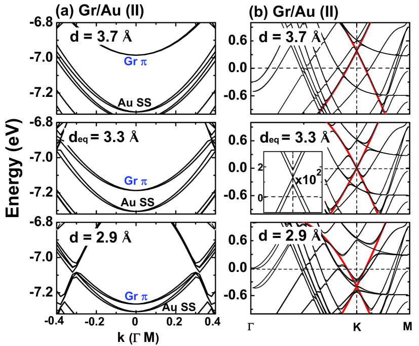
Figure 3 shows the energy bands in large energy range for Gr/Au with configuration (II) at equilibrium distance. The two sets of parabolas at about -0.2 and -0.4 eV around the point are the Au (111) SSs at the two sides of the Au slab, with and without graphene, respectively. They are degenerate at -0.4 eV for the pure Au (111) filmnico , but now the SS in the side with the adsorption of graphene is pushed up slightly. In comparison with Fig. 1(b), the bulk Au 5 bands around point (about -2-7 eV) are deeper in energy than Ni 3 bands. This bestows the probability for Au 5 to strongly interact with graphene bands, which are in a big interstice formed mainly by Au 5 states. The situation is very different from that in Fig. 1(b), where the graphene and Ni 3 states are well separated in energy. To understand the different SO splittings in Ni and Au cases, wave function compositions of the bands at are analyzed quantitatively. As shown in Table I, the ratio of C 2:Ni 4 in Gr/Ni (I) 1.0:0.8; no Ni 3 is involved. Since Ni 4 states do not contribute to the SO effect, the enhancement of Rashba splitting in Gr/Ni only results from the asymmetric potential distribution in the two sides of graphene. In contrast, contribution from the Au state is obvious for Gr/Au (II); the ratio of C 2:Au 6:Au 5 is about 1.0:1.3:2.4. Therefore, strong hybridization of the metal with graphene is a key factor to produce large SO splitting in graphene bands.
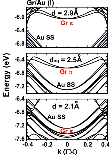
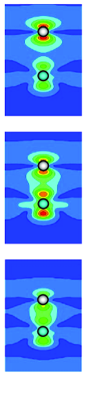
For Gr/Au, configuration (I) is less stable than configuration (II) since the C-C bonds in graphene have to be stretched by 17% to match the structure of the Au (111) substrate. This stretching gives rise to a much shorter equilibrium distance (2.5 Å) in the interface, and thus allows us to understand the effects of adjusting the lateral and vertical distances. The whole bands of graphene in the configuration (I) thus disperse less; and shift upward as well, hopefully causing more effective hybridization between C 2 and Au 5 states. Figure 4 gives the SO splitting of the graphene bands in Gr/Au (I) at deq to be close to 100 meV, 3 times larger than that in Au (II) case. In Gr/Au (I), the Au 6 component decreases meanwhile the C 2 and the Au 5 more effectively hybridize to each other (see Table I), as expected. Similar to the trend in Fig. 2(a) either, increasing or decreasing d cause a decrease of the SO splitting in Fig. 4. This trend can be rationalized by using the real-space charge densities of the graphene bands at in the right panels of Fig. 4. At the equilibrium distance, a very obvious interaction between graphene and metal and asymmetric charge distribution above and below the graphene plane are observed, corresponding to large SO splitting. When d becomes longer or shorter than deq, the effective mixing between C and Au is weakened.
Table I also contains the results of Gr/Ag (I) and (II). Again, the SO splitting in the configuration (II) is much less than that in (I) due to weakened hybridization. While the graphene state has strong interaction with the Ag state in the configuration (I), only Ag state is involved in the more stable Gr/Ag (II), similar to Ni. Therefore, heavy metals may not always produce large SO splitting in graphene.
| meV | Ni (I) | Au (II) | Au (I) | Ag (II) | Ag (I) |
|---|---|---|---|---|---|
| N = | |||||
| N = |
Finally, we also explored the effect of the thickness of metal films. The SO splitting of graphene bands for Gr/Au (I) and (II) and Gr/Ag (I) with N=6 in Table II are almost the same as the values listed in Table I, respectively. For the rest two cases: Gr/Ni (I) and Gr/Ag (II), only one monolayer of metal substrate is enough to give a saturated SO splitting of graphene. Since Au SSs usually extend several atomic layers into the bulkliu , a few layers of metals are needed to obtain the saturated SO splitting. Nevertheless, the SO splitting for graphene on Au mono- and bi-layer films is already large, explaining why one Au atomic layer intercalated between graphene and Ni (111) can cause a substantial Rashba effect in the experiment.va
In conclusion, we investigated what determines the SO splitting of graphene bands on Ni, Au, or Ag (111) substrates through first-principles calculations. While the Rashba splitting for Gr/Au is sizeable, the effect of Ni is very limited. The hybridization between graphene and metal states is identified as the chief factor for the enhancement of the SO effect in graphene. This requires not only large SO strength from metal atoms, but also effective overlap of metal d and graphene states in energy. A few atomic layers of metals are sufficient to produce saturated strong Rashba splitting in graphene. Our findings point out a direction for the manipulation of SO strength in graphene that is needed for the development of spintronic materials and devices.
The work was supported by National Natural Science Foundation of China (No.10674027), 973 project (No.2006CB921300), Fudan High-end Computing Center, and Chemistry and Materials Research Division (MRSEC program) of NSF in USA. Work at UCI was supported by DOE grant DE-FG02-05ER46237 and computing time at NERSC.
References
- (1) A. H. Castro Neto, F. Guinea, N. M. R. Peres, K. S. Novoselov and A. K. Geim, Rev. Mod. Phys. 81, 109 (2009).
- (2) K. S. Novoselov, A. K. Geim, S. V. Morozov, D. Jiang, M. I. Katsnelson, I. V. Grigorieva, S. V. Dubonos, and A. A. Firsov, Nature (London) 438, 197 (2005).
- (3) Y. Zhang, Y.-W. Tan, H. L. Stormer, and P. Kim, Nature (London) 438, 201 (2005).
- (4) N. Tombros, C. Jozsa, M. Popinciuc, H. T. Jonkman, and B. J. van Wees, Nature (London) 448, 571 (2007).
- (5) Y. G. Semenov, K. W. Kim, and J. M. Zavada, Appl. Phys. Lett. 91, 153105 (2007).
- (6) S. Datta and B. Das, Appl. Phys. Lett. 56, 665 (1990).
- (7) D. D. Awschalom and M. E. Flatté, Nature Phys. 3, 153 (2007).
- (8) C. L. Kane and E. J. Mele, Phys. Rev. Lett. 95, 226801 (2005).
- (9) F. Kuemmeth, S. Ilani, D. C. Ralph, and P. L. McEuen, Nature (London) 452, 448 (2008).
- (10) Y. Yao, F. Ye, X.-L. Qi, S.-C. Zhang, and Z. Fang, Phys. Rev. B 75, 041401(R) (2007).
- (11) E. I. Rashba, Sov. Phys. Solid State 2, 1109 (1960); Yu. A. Bychkov and E. I. Rashba, JETP Lett. 39, 78 (1984).
- (12) Yu. S. Dedkov, M. Fonin, U. Rüdiger, and C. Laubschat, Phys. Rev. Lett. 100, 107602 (2008).
- (13) O. Rader, A. Varykhalov, J. Sánchez-Barriga, D. Marchenko, A. Rybkin, and A. M. Shikin, Phys. Rev. Lett. 102, 057602 (2009).
- (14) G. Kresse and J. Furthmüller, Phys. Rev. B 54, 11169 (1996); G. Kresse and J. Hafner, Phys. Rev. B 49, 14251 (1994).
- (15) J. P. Perdew and Y. Wang, Phys. Rev. B 45, 13244 (1992).
- (16) E. Durgun, R. T. Senger, H. Sevinçli, H. Mehrez, and S. Ciraci, Phys. Rev. B 74, 235413 (2006).
- (17) V. M. Karpan, G. Giovannetti, P. A. Khomyakov, M. Talanana, A. A. Starikov, M. Zwierzycki, J. van den Brink, G. Brocks, and P. J. Kelly, Phys. Rev. Lett. 99, 176602 (2007).
- (18) G. Giovannetti, P. A. Khomyakov, G. Brocks, V. M. Karpan, J. van den Brink, and P. J. Kelly, Phys. Rev. Lett. 101, 026803 (2008).
- (19) G. Nicolay, F. Reinert, S. Hüfner, and P. Blaha, Phys. Rev. B 65, 033407 (2001).
- (20) G. Bertoni, L. Calmels, A. Altibelli, and V. Serin, Phys. Rev. B 71, 075402 (2005).
- (21) A. Nagashima, N. Tejima, and C. Oshima, Phys. Rev. B 50, 17487 (1994).
- (22) I. Gierz, J. H. Dil, F. Meier, B. Slomski, J. Osterwalder, J. Henk, R. Winkler, C. R. Ast, and K. Kern, arXiv:1004.1573v1.
- (23) S. H. Liu, C. Hinnen, C. Nguyen Van Huong, N. R. De Tacconi, and K. M. Ho, J. Electroanal. Chem. 176, 325 (1984).
- (24) A. Varykhalov, J. Sánchez-Barriga, A. M. Shikin, C. Biswas, E. Vescovo, A. Rybkin, D. Marchenko, and O. Rader, Phys. Rev. Lett. 101, 157601 (2008).
- (25) A. Yamakage, K.-I. Imura, J. Cayssol, and Y. Kuramoto, Europhys. Lett. 87, 47005 (2009).