Design Study for a Super Pixel Vertex Detector
Abstract
We present a conceptual design for a low-mass, all-pixel vertex detector using the CMOS quadruple well INMAPS process, capable of working in the very high luminosities exceeding that can be expected at the next generation Factories. We concentrate on the vertexing requirements necessary for time-dependent measurements that are also relevant to searches for new physics beyond the Standard Model. We investigate different configurations and compare with the baseline designs for the Super and BABAR experiments.
keywords:
Vertex detector , SuperB , MAPS , pixels1 Introduction
This document summarises the conceptual design and the supporting physics studies for an all-pixel vertex detector to be considered at the proposed next generation high luminosity collider called Super [1, 2]. We give a short introduction to the physics case for Super and the motivation for an all-pixel vertex detector based on MAPS technology. We describe the pixel sensor design parameters in section 2 and the mechanical support structure in section 3. In section 4, we discuss a number of options for different geometries and use the simulated decay channel to characterise the performance of the vertex detector in terms of its time resolution and -flavour tagging efficiency. More information on Super can be found in the Super Detector ‘White Paper‘ [1], the Conceptual Design Report [2], and the proceedings of the SLAC Workshop on a Super Flavour Factory [3].
Super is a next generation high luminosity collider Factory that exploits small beam emittances ( and ) to deliver high luminosities with moderate currents of A and an estimated power consumption of less than 20 MW [4, 5]. The luminosity will be above , a factor 100 greater than today’s Factories, allowing a data sample of 75 to be accumulated within five years of nominal running.
Super will perform precision tests of the Standard Model and searches for new physics phenomena. For example investigations of the current deviations from the Standard Model predictions at the level of from the existing Factories, BABAR and Belle.
The ability of Super to look for new physics signals through indirect searches is complementary to the direct searches that are underway at the Large Hadron Collider (LHC). Super can also search for new physics at scales beyond the reach of the LHC. Precision tests of Charge-Parity-Time (CPT) conservation at Super will probe new physics at the Planck scale. CP violation parameters in and decays are sensitive probes of Higgs and Super-Symmetric (SUSY) particles. Super can combine information from rare decays to precisely measure (the ratio of the Higgs-doublet vacuum expectation values) or the coupling in Constrained Minimal Super-Symmetric Models (CMSSM). Super can also search for charged Higgs particles to a level that exceeds the LHC search capabilities by a factor of 3-5 over the full range of . Using rare decays Super will be able to measure flavour couplings in the squark sector to a few percent. Super will search for Lepton Flavour Violation (LFV) in the decays of the -lepton down to branching fractions of the level of ; SUSY Grand Unified Theory (GUT) models, using constraints from the current mixing and phase measurements from the Tevatron, predict that LFV decays could exist with branching fractions of a few [6].
The Super detector is a refinement on the BABAR design and described in detail in [7]. As Super will operate at a lower centre of mass boost, (6.7 beam against a 4.2 beam), the average spatial vertex separation between the two decaying mesons is , a factor of two smaller than BABAR.
For its vertex detector, Super plans to use a similar design as the BABAR detector, with five layers of silicon strips with a radius between 3 and 15, but with an additional inner layer of striplets at a radius of to the beam (Layer 0). The Layer 0 is the biggest challenge for the design of the Super silicon vertex detector. Super simulations suggest a maximum hit rate in Layer 0 of . This high data rate and the associated power consumption require an active cooling solution while still maintaining a small material budget. The radiation damage at Super is also an issue with the expected radiation dose for Layer 0 of Mrad, corresponding to 1013 neutrons. Up to now, there have been several proposals to realise Layer 0, based on either LHC-style hybrid pixels [8] or striplets [9].
Our proposal is to replace the current six layer design of Super with a six layer solution using pixels for all the layers with a pixel size of , corresponding to 2500 hits per second per pixel for Layer 0. This is made possible by using Monolithic Active Pixel Sensor (MAPS) technology [10]. To simplify assembly and testing we are planning to use a long barrel design with the sensors mounted on a stave structure with integrated cooling. This will allow easy exchange of a stave in case of problems e.g. a massive beam incident. An homogeneous detector using the same solution everywhere will make construction and maintenance easier. However an all-pixel solution for the vertex detector poses a challenge as both high granularity and a low material budget are important.
2 Sensor Design
This Super pixel design study is based on circuitry already developed for the Tera-Pixel Active Calorimeter (TPAC) chip [11]. This design is intended to be used in a digital electromagnetic calorimeter for the International Linear Collider (ILC) [12, 13]. Also considered is the more advanced four-transistor (4T) architecture already explored in the Fortis chip [14]. Each Super chip is assumed to be in size, and four chips are stitched together to make a module with an active area of , and a pixel size of . The hits in the silicon pixels are also to be used in measurements, so an ADC with 4-5 bit resolution is required. The readout is based on a column architecture with the electronics at the short end of the module. Each chip has one million pixels and each module therefore has four million pixels with 2000 columns and 500 pixels per column. The raw data rate per module is 10 , assuming a hit rate of 2500 hits per second per pixel and a data size of 32 bits per pixel (row/column address plus time stamp and 5-bit ADC value). This illustrates the need for on-chip data reduction. As timing information is required, the chips will be sampled every 500, providing enough granularity in time to provide efficient pattern recognition in Layer 0.
The TPAC chip has been designed using the 180 CMOS quadruple well INMAPS process [11], which includes a deep p-well implant. This allows the use of full CMOS capabilities, as the n-wells of the PMOS devices are now shielded by the deep p-well. This is a significant advantage to previous MAPS devices which were limited to the use of NMOS technology because of the parasitic charge collections of the PMOS n-wells.
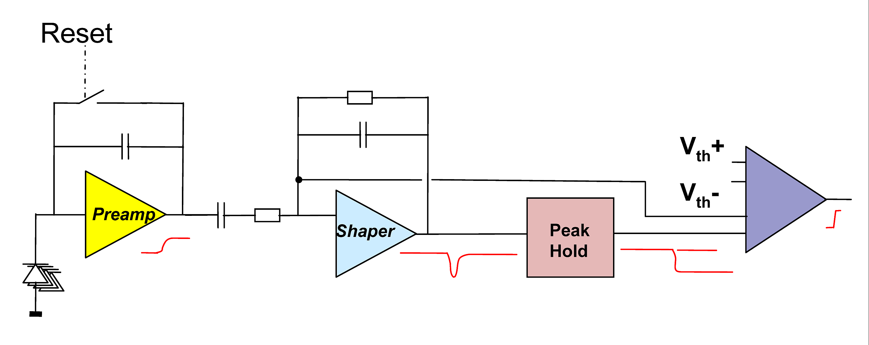
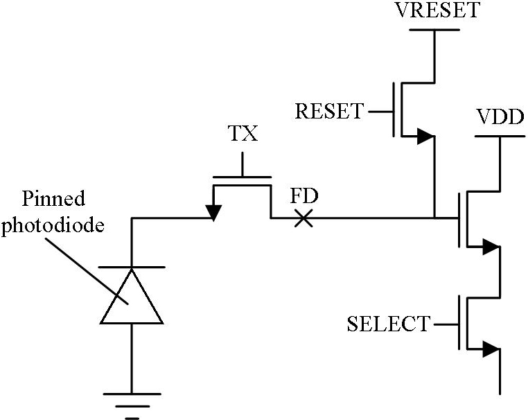
The original TPAC pixel contains a preamplifier, a shaper and a comparator [11]. The pixel only stores hit information in a 14-bit “Hit Flag”. The pixel itself runs without a clock and the timing information is provided by the logic querying the “Hit Flag”. For the Super application, a peak-hold latch was added as shown in Fig. 1 to store the analog information as well. The chip is organised in columns with a common ADC at the end of each column. The ADC is realised as a 5-bit Wilkinson ADC using a 4 clock. For the predicted time-stamping resolution of 500, there are on average 1.25 pixels hit in a column. The simulated power consumption for each individual pixel is less than and the power consumption per module is smaller than 12 W.
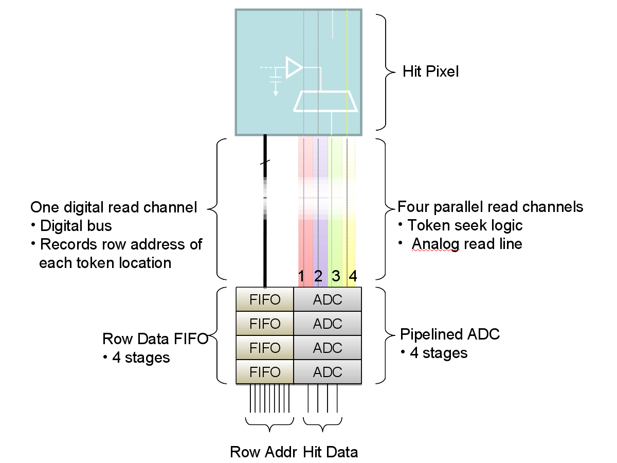
The column logic constantly queries the pixels for their “Hit Flag” (Token Seek logic) but only digitises the information for the pixels with a “Hit Flag” high. This saves both space and reduces the power usage. Since the speed of the chip is limited by the ADC, the Token Seek logic also increases the readout speed. Both the address of the pixel being hit and its ADC output are stored in a FIFO at the end of the column. This is shown in Fig 2.
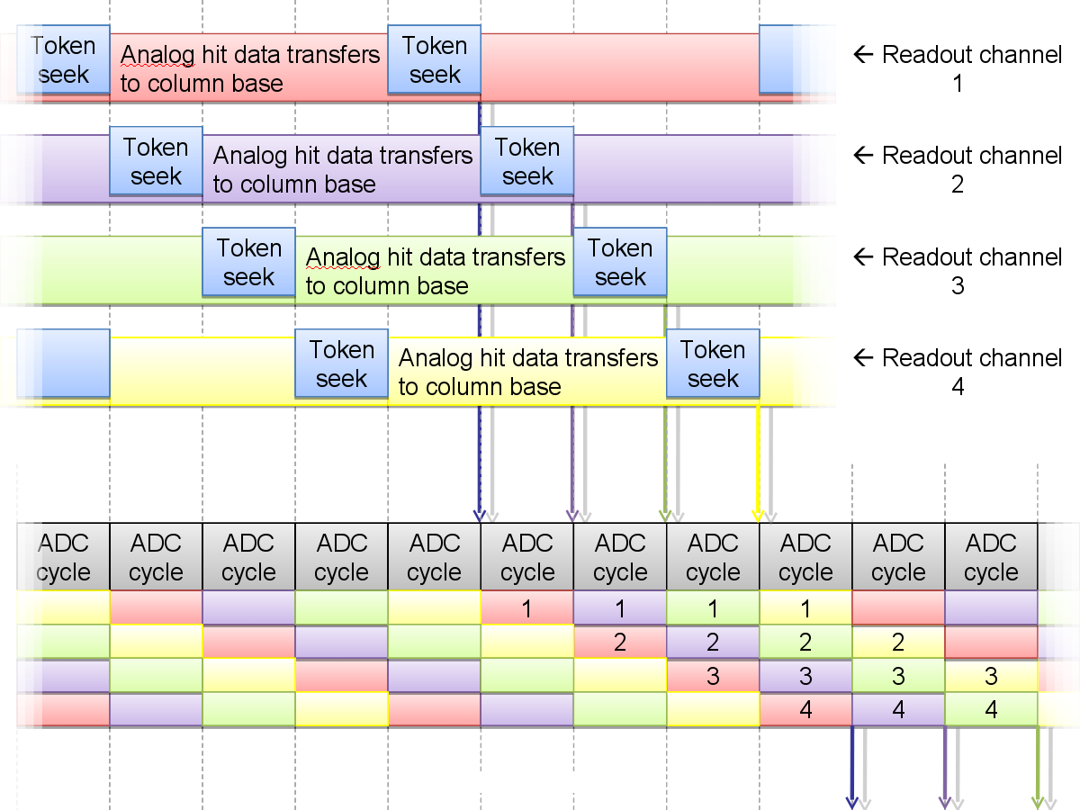
As the analog charge transfer from the individual pixels to the end of the column is slow, the ADC uses a pipelined architecture with 4 analog input lines to further increase throughput of the ADC. The pipeline design is illustrated in Fig. 3.
One of the main bottlenecks is reading the data from the module. The minimum irreducible event rate in the detector is expected to be 50 from Bhabha scattering and 20 from physics production [1]. A hardware-based Level 1 trigger will receive data at 4 , using information from the drift chamber and calorimeter, and will accept events for further processing at a design limit of 150 . Readout of the vertex detector will only happen on receipt of the Level-1 Accept signal and this will reduce the data rate by a factor of 10. This also minimises power and services required, as shown in Fig. 4.
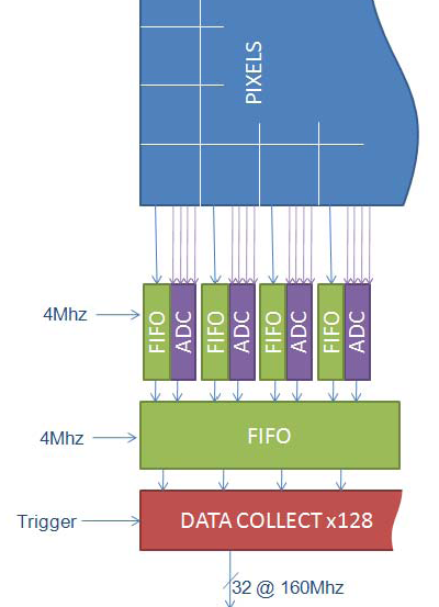
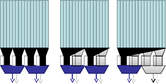
For the outer layers, the hit rate is much smaller and the timing requirements can be relaxed. To save power, the ADCs in these layers will be multiplexed to handle more than one column in the sensor. A multiplexing scheme for this device is also illustrated in Fig. 4.
An alternative to the TPAC chip is a four transistor (4T) structure as has already be demonstrated by the Fortis chip [14]. This would allow ultra-low noise performance on a level of less than eight electrons, a much smaller power consumption of about 2W per pixel and the possibility of pixel sizes less than . The limiting factor for this approach is the speed of the charge transfer in the 4T structure (see Fig. 5), which is currently limited to 1-2 s. If Correlated Double Sampling (CDS) is used to reduce the noise, a second readout is required and so the total readout time is 2-4 which is close to the trigger accept limit. Fast charge transfer structures would need to be added in order to satisfy the Super timing requirements.
The TPAC chip uses standard industry processes and this significantly reduces the production costs. Yields of at least 60 % are achievable for these sensors. Even when set-up costs are taken into account, it is still financially feasible to regularly replace the sensors in the inner layer, eliminating the need for extreme radiation hardness.
3 Mechanical Design
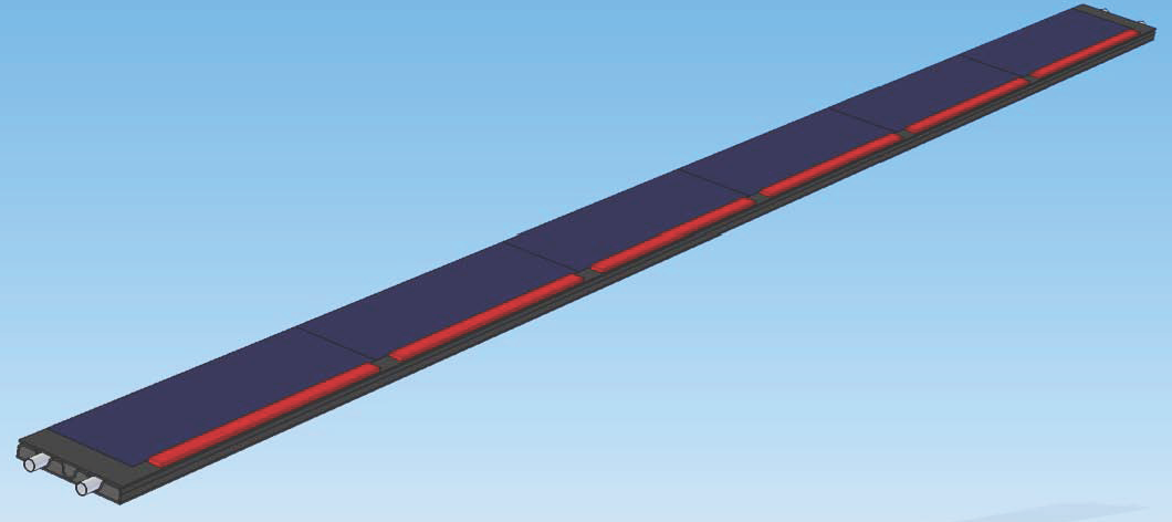
The mechanical concept outlined here is for a barrel detector geometry built from units of modules arranged on staves. Each sensor module consists of 4 chips and has a size of with a thickness of 50 . This forms the irreducible unit that the remainder of the detector is constructed from. Figure 6 shows the stave concept for the outermost layer. The cooling, power and readout is connected to the stave at one or both ends, to facilitate installation and replacement should modules fail for any reason. The coolant is assumed to be water, and in order to maintain suitable operational conditions we need to be able to extract about of power from each sensor module, which corresponds to . The cooling pipes are assumed to be made from thin walled Al tube, however it may be possible to try alternative pipe materials if there is a significant reduction in the material budget.
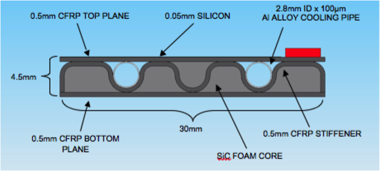
The material budget for this design is shown in Table 1. The sensor consists of INMAPS active material with a 50 thick layer of implanted silicon; a carbon fibre support structure (CFRP); an Aluminium cooling pipe; coolant (water); and a SiC Foam (4% density) modeled as an equivalent amount of Carbon Fibre. The majority of the material in the stave is Carbon Fibre. This design is rigid, with a 250 sag over a distance of 60, which is the maximum distance between support structures in the outer layer. The total material budget conservatively corresponds to a total radiation length of . This is adequate in the outer layers but has a detrimental effect in the inner layers. The inner most layer(s) could benefit from a significantly lower mass support structure. An ultra-low mass support for Layer 0 using a peek-carbon fibre support layer with has been proposed [15] and we are considering this design as an alternative.
| Substance | Thickness | Radiation | Radiation |
|---|---|---|---|
| (mm) | length (mm) | length (%) | |
| Silicon | 0.05 | 94 | 0.053 |
| CFRP | 1.752 | 240 | 0.730 |
| Al | 0.0623 | 89 | 0.069 |
| Water | 0.41 | 360 | 0.114 |
| SiC | 1.81 | 1000 | 0.181 |
| Total | 1.147 |
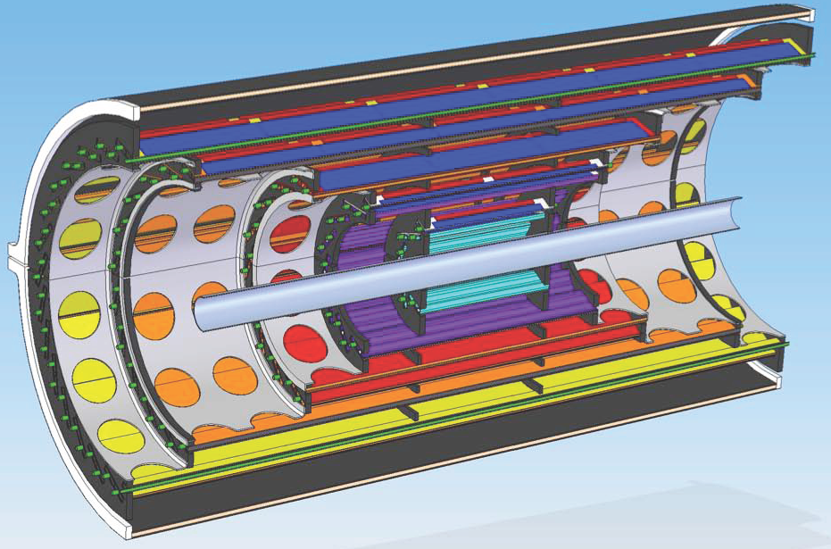
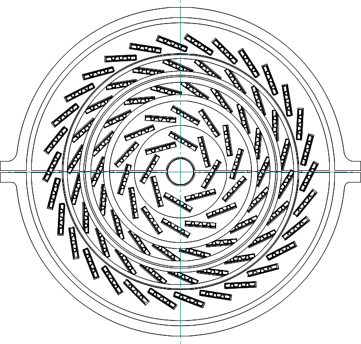
The baseline geometry for the Super vertex detector assumes a lamp-shade design similar like the Babar vertex detector design [7], where the ends of the outer layers are angled with respect to the beam line to reduce the multiple scattering for low angle tracks. Here we have considered a long barrel detector with many staves joined together in two detector halves. These two halves are brought together in the final detector. This has the advantage of uniform modules. However as low angle tracks will pass through more material in a long barrel detector, this design can suffer from higher multiple scattering for such tracks. However the depth of the charge collection in the sensor is sufficiently small that this is not the major error on the track measurements. Fig. 7 shows a cut-away view of one half of the detector for a five layer design. Also shown is a sectional view of the detector illustrating the overlapping layout of the individual staves.
4 Physics Studies
We have studied the performance of the Super detector with different geometries of a vertex detector, ranging from the Super baseline, through to a four or six layer all-pixel detector with a realistic material budget for the support structure for all layers. The decay channel chosen for these studies is , where one of the decays through the channel , as this tests the ability to reconstruct tracks and identify the positions of the two mesons when they decay. A critical aspect of the detector is the ability to compute the proper time difference between the decays of the two mesons in the event, as computed from the reconstructed spatial separation between the vertices and the known boost of the experiment. The signal reconstruction efficiency for these events and the resolution on are used to compare a number of different vertex detector geometries, with the rest of the detector assumed to be the baseline as outlined by the Super CDR [2]. A good resolution is vital for Super to measure accurately the asymmetry parameters and , which in turn can be used to search for new physics for a number of rare final states of a meson. The vertex detector must also be able to identify the flavour of the other in the event (the “tagged ”) in order to make time-dependent measurements, as well as a number of other new physics searches that will be performed at Super. This requires in particular efficient reconstruction of pions with low transverse momentum (). This benchmark decay is therefore a validation of both searches for new physics and Standard Model calibration measurements, and is a good indicator of performance across a wide-range of physics channels.
All studies documented here use the Super Fast Simulation V0.1.1 [1]. Events are selected using the same analysis criteria as the BABAR analysis [16]. The simulation assumes a boost , which is slightly larger than the boost currently foreseen.
We have considered the following geometries:
-
1.
The baseline Super geometry [Super Baseline].
-
2.
The BABAR geometry with the PEP-II beam conditions [BABAR Baseline].
-
3.
A 6-layer all Hybrid Pixel detector (layers: ) [Hybrid Pixels].
-
4.
A 4-layer all Hybrid Pixel detector (layers: ) [Hybrid Pixels-4A].
-
5.
The baseline Super geometry with an INMAPS detector for Layer 0 [INMAPS-L0].
-
6.
A 6-layer all-pixel INMAPS detector (layers: ) [INMAPS].
-
7.
A 4-layer all-pixel INMAPS detector (layers: ) [INMAPS-4A].
-
8.
A 4-layer all-pixel INMAPS detector with layers at 1.6, 5, 10.2 and 14.2 radii) [INMAPS-4B].
-
9.
A 6-layer all-pixel INMAPS detector with a low mass Layer 0 support (layers: ) [INMAPS-LL0].
The first two geometries serve as baselines in order to evaluate the performance expected from an all-pixel INMAPS based silicon detector. The two geometries using Hybrid Pixel technology require more material than INMAPS and are used only to provide a bound for any possible effects of underestimation of the material budget for the cooling and the support structure. Geometries five to eight cover various alternative layouts for the number and radii of an all-pixel INMAPS detector with each layer having the material budget shown in Table 1. The last geometry uses the INMAPS material budget for the outer layers and the ultra-low mass support for Layer 0 ().
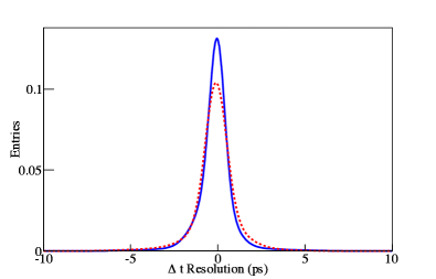
Table 2 summarises the resolution for the benchmark channel for the nine geometries considered. The distribution for events with both decays reconstructed is fitted with a function consisting of three Gaussians. The table shows the Root Mean Squared (RMS) and the Full-Width Half-Maximum (FWHM) of the distribution. represents the fraction of the fitted function that is assigned to the Gaussian with the smallest width . Smaller widths and larger indicate better performance. The all-pixel detector geometries are clearly compatible with the Super baseline in terms of their resolution (geometries five to eight) and such a detector with a low mass support structure for Layer 0 (geometry 9) is superior to this, and gives a similar resolution to as the existing BABAR detector (geometry 2). A comparison of the resolution function obtained for this sample, with respect to the Super baseline is shown in Figure 8. Overall, the all-pixel detector in its various configurations is between 12% and 20% better than the baseline in terms of the RMS or FWHM, while still maintaining the same signal reconstruction efficiencies and energy resolutions.
| Configuration | RMS () | FWHM () | () | ||
|---|---|---|---|---|---|
| 1 | Super Baseline | 1.44 | |||
| 2 | BABAR Baseline | 1.33 | |||
| 3 | Hybrid Pixels | 1.54 | |||
| 4 | Hybrid Pixels-4A | 1.49 | |||
| 5 | INMAPS-L0 | 1.40 | |||
| 6 | INMAPS | 1.42 | |||
| 7 | INMAPS-4A | 1.32 | |||
| 8 | INMAPS-4B | 1.29 | |||
| 9 | INMAPS-LL0 | 1.14 |
We have computed the efficiency for identifying the flavour of the decays ( or ) as a function of six pre-defined tagging categories that correspond to different types of events. Each category uses information from the reconstructed tag side to identify the flavour of the other . In order of increasing mis-tag probability they are: the “Lepton” category using fast leptons (); “Kaon 1” using tracks clearly identified as charged kaons through particle identification (PID) techniques; “Kaon 2” using tracks with a lower probability of being a kaon; “Pion” using tracks clearly identified as charged pions; the “Other” category using other information of a lower quality; and “Untagged” which represents all events which do not fall into the previous five.
The best single metric for comparing the geometries is the total tagging efficiency . However, this requires information on the dilution factor for each tagging category which is not available for the Super simulations. As an alternative we look at the efficiencies for the individual categories. The Lepton flavour tag is the most important category as it has the lowest mis-tag fraction but the other categories are also vital contributors to the overall efficiency.
Table 3 summarises the tagging efficiencies for the different detector configurations. The efficiencies for geometries two to nine are given relative to the Super baseline design. This accounts for differences between the tagging algorithm implemented in this simulation and numbers reported elsewhere by BABAR and Super. From this table we can see that the Super baseline lepton tag efficiency is consistent with the BABAR one but the Pion and Other tagged categories are lower in efficiency and the Super baseline will have more untagged events. The four layer detector geometries reduce the efficiency for lepton tagged events by from the baseline. The INMAPS detector has an efficiency comparable with the Super baseline for lepton tagged events. There is some small variation in the untagged category efficiency as a function of geometry, however this is typically at the 0.4% level.
| Configuration | Lepton | Kaon 1 | Kaon 2 | Pion | Other | Untagged | |
|---|---|---|---|---|---|---|---|
| 1 | Super Baseline | 0.0390.002 | 0.1080.002 | 0.1280.003 | 0.1760.003 | 0.1100.002 | 0.4400.004 |
| 2 | BABAR Baseline | 0.9490.054 | 1.0280.036 | 1.0550.030 | 1.1420.025 | 1.1640.031 | 0.8840.015 |
| 3 | Hybrid Pixels | 0.9230.056 | 0.9810.038 | 1.0470.030 | 1.0060.028 | 0.9820.037 | 1.0000.014 |
| 4 | Hybrid Pixels-4A | 0.7180.071 | 1.0000.037 | 0.9220.034 | 0.9150.031 | 0.9180.040 | 1.1030.012 |
| 5 | INMAPS-L0 | 0.8970.057 | 1.0090.037 | 1.0230.031 | 0.9830.029 | 0.9360.039 | 1.0230.013 |
| 6 | INMAPS | 0.9230.056 | 1.0090.037 | 1.0160.031 | 0.9890.029 | 0.9820.037 | 1.0090.014 |
| 7 | INMAPS-4A | 0.6920.074 | 1.0000.037 | 0.9450.033 | 0.9430.030 | 0.9450.038 | 1.0800.013 |
| 8 | INMAPS-4B | 0.7690.067 | 1.0000.019 | 1.0000.023 | 1.0000.017 | 1.0000.018 | 1.0210.009 |
| 9 | INMAPS-LL0 | 0.8720.059 | 1.0280.036 | 0.9690.032 | 1.0060.028 | 1.0000.036 | 1.0110.014 |
5 Conclusion
These initial studies suggest that a four layer all-pixel INMAPS vertex detector will be as performant as the current Super baseline geometry. A low mass support for Layer 0 would further offset any performance degradation obtained by halving the boost of the centre of mass system required by the power budget of the Super accelerator. A six layer all-pixel INMAPS vertex detector using this support structure for the inner layer would have a resolution comparable to BABAR. The energy resolution and event reconstruction efficiency for is independent of the amount of material in the detector but it will be important to study the effect of material on final states with neutral particles as a complementary input to the detector optimisation. In addition more studies are required for time-dependent CP analyses, charm mixing, and other channels that depend highly on slow pion efficiency.
The long barrel design can be improved by combining the support structure for the outer layers four and five and so reducing the amount of material required. A lamp-shade structure, to reduce multiple-scattering at low angles, can also be designed without the need to resort to non-standard industry chip dimensions. Both concepts are under study.
This R&D effort has produced a viable pixel vertex detector design for the Super detector that meets the challenging demands placed on the system in terms of rate and delivers superior physics performance when compared to other viable alternative technologies. This design concept has been developed with uniformity in mind. Further R&D is required to realise a prototype module and stave structure for further tests. Preliminary tests with X-rays have produced satisfactory results for the existing TPAC layout but the design would benefit from further radiation tests to confirm that the sensors will perform as expected in terms of bulk damage when exposed to Mrad radiation dose. However, the low production costs of the sensor offer the possibility of a design with a disposable inner-layer that is replaced each year.
6 Acknowledgements
This work has been supported by the Science and Technology Facilities Council (STFC).
References
- [1] E. Grauges, F. Forti, B. N. Ratcliff and D. Aston , “SuperB Progress Reports – Detector,” arXiv:1007.4241 [physics.ins-det].
- [2] M. Bona et al., Super Conceptual Design Report (2007), INFN/AE-07/2, SLAC-R-856, LAL 07-15, arXiv:0709.0451.
- [3] Joanne L. Hewett et al., “The Discovery Potential of a Super Factory”, SLAC-R-709 (2004).
- [4] P. Raimondi in “2nd LNF Workshop on Super”, Frascati, Italy, March 16-18 2006 http://www.lnf.infn.it/conference/superb06/; and in Proceedings of Particle Accelerator Conference (PAC 07), Albuquerque, New Mexico, USA, June 25-29, 32 (2007).
- [5] “Design Progress Report for the Super Accelerator”, (2010), in preparation.
- [6] B. O’Leary et al., “SuperB Progress Reports – Physics,” arXiv:1008:1541.
- [7] B. Aubert et al., Nucl. Instrum. Methods Phys. Res., Sect. A 479 1 (2002).
- [8] G. Aad et al., JINST 3 (2008) P07007; D. Kotlinski et al., JINST 4 (2009) P03019; K. Aamodt et al., JINST 3 (2008) S08002.
- [9] L Vitale et al., Nucl. Instrum. Methods Phys. Res., Sect. A 617, 601-604 (2010).
- [10] R. Turchetta et al., Nucl. Instrum. Methods Phys. Res., Sect. A 458, 677-689 (2001).
- [11] J. A. Ballin et al., “Monolithic Active Pixel Sensors (MAPS) in a quadruple well technology for nearly 100% fill factor and full CMOS pixels,” Sensor 2006,6.
- [12] N. K. Watson et al., “A MAPS-based readout of an electromagnetic calorimeter for the ILC,” J. Phys. Conf. Ser. 110 (2008) 092035.
- [13] J. P. Crooks et al., “A monolithic active pixel sensor for a tera-pixel ECAL at the ILC,” CERN-2008-008.
- [14] R. Coath et al., “Advanced Pixel Architectures for Scientific Image Sensors”, CERN-2009-006.
- [15] G. Balestri et al., Nucl. Instrum. Methods Phys. Res., Sect. A 617 526-529 (2010).
- [16] B. Aubert et al., Phys. Rev. D 75, 012008, 2007.