Superconducting RF Metamaterials Made with Magnetically Active Planar Spirals
Abstract
Superconducting metamaterials combine the advantages of low-loss, large inductance (with the addition of kinetic inductance), and extreme tunability compared to their normal metal counterparts. Therefore, they allow realization of compact designs operating at low frequencies. We have recently developed radio frequency (RF) metamaterials with a high loaded quality factor and an electrical size as small as , ( is the free space wavelength) by using Nb thin films. The RF metamaterial is composed of truly planar spirals patterned with lithographic techniques. Linear transmission characteristics of these metamaterials show robust Lorentzian resonant peaks in the sub- 100 MHz frequency range below the of Nb. Though Nb is a non-magnetic material, the circulating currents in the spirals generated by RF signals produce a strong magnetic response, which can be tuned sensitively either by temperature or magnetic field thanks to the superconducting nature of the design. We have also observed strong nonlinearity and meta-stable jumps in the transmission data with increasing RF input power until the Nb is driven into the normal state. We discuss the factors modifying the induced magnetic response from single and 1-D arrays of spirals in the light of numerical simulations.
Index Terms:
RF metamaterials, superconducting devices, artificial magnetic response.I Introduction
Metamaterials are engineered structures composed of sub-wavelength artificial unit cells that form a homogeneous effective medium for the electromagnetic waves propagating through them. This effective response can be described by a coarse-grained electric permittivity and the magnetic permeability [1]. By manipulating these two electromagnetic parameters, interesting properties unavailable in nature have been demonstrated, such as negative refractive index [2] and artificial magnetism [3, 4].
Most metamaterials are designed to give a magnetic response at microwave or higher frequency bands [2, 5]. They usually employ split ring resonators (SRRs), or their derivatives, and can be generally understood with a lumped-element inductor-capacitor circuit model [2].
As the wavelength, , of the electromagnetic waves increases towards the radio frequency (RF) band, miniaturizing the inclusions forming a metamaterial becomes more challenging [6]. The Swiss Roll metamaterial [6], a three dimensional (3-D) geometry which inspired the SRR design, has achieved a reasonable magnetic response in the sub-100 MHz band. Since the design is implemented with normal metals (thick Cu sheets separated by dielectrics), ohmic losses and bulkiness are the limiting factors.
II The Design
Our Nb RF metamaterials are constructed from micro-structured 2-D spirals. Earlier experiments [11, 12] utilized planar spirals made of thick Cu films (35 m thick in [11] and 0.25 mm thick in [12]) on dielectric substrates. Such thick coatings are required to minimize Ohmic losses, making the design intermediate between 2-D and 3-D. Further reduction of the resonant frequency of such spirals is not possible due to the scaling of Ohmic dissipation with spiral length.
Because the electrical size of the elemental spiral is significantly smaller than the operating wavelength, a quasi-static approach can be used, and the design can be based on a lumped element analogy as in SRRs [13]. The large number of turns gives a significant geometrical inductance, [14] and the spacing between them provides substantial capacitance, [15]. Therefore, the geometry can be kept compact enough to achieve a sub-100 MHz resonance frequency, (despite the large ). Since the design is realized with superconducting films, there is an additional term called kinetic inductance, [16] which is closely linked to the superfluid density. For example, when the transition temperature, , is approached, the superfluid density goes to zero, and can make the dominant contribution to the total inductance, resulting in a significant reduction in .
III Sample Preparation
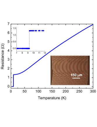
The fabrication starts with the deposition of 200 nm Nb thin films on 350 m thick quartz substrates, 3” in diameter, by the RF sputtering technique [17]. The transition temperature of the film is found to be K from resistance measurements taken by a Physical Property Measurement System (PPMS) [18]. The main panel of Fig. 1 shows the resistance of the Nb film for a wide range of temperature from 300 K down to 1.5 K, whereas the top-left inset focuses on the transition region. The Nb film is patterned into a spiral geometry by photolithography and reactive ion etching. The etching is performed by a chemically active mixture of \ceCF4/\ceO2 (10 \ceO2). The wafer is diced into chips having single spirals and into 1-D arrays composed of various numbers of spirals. An optical image of one of the single spirals giving sub-100 MHz resonant features with an outer diameter of 6 mm and N = 40 turns is shown in the bottom-right inset of Fig. 1. The width of the stripes and spacing between them are equal and each is 10 m.
IV Building Blocks of the RF Metamaterial: The Single Spiral
IV-A Transmission Data
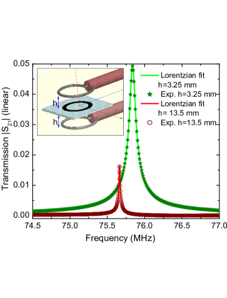
The RF transmission measurements are carried out on single elements of our RF metamaterials in an evacuated cryostat at temperatures ranging from 300 K down to 4.2 K. The sample is mounted between two RF magnetic loop probes, 6 mm in diameter, whose axes are parallel to each other and the Nb spiral, as shown in the inset of Fig. 3. The spiral resonator is excited by the top probe providing the RF signal and the transmission is picked up by the bottom probe. Both loop probes are connected to an Agilent E5062A RF network analyzer.
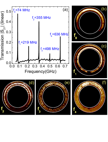
The full transmission spectrum on a single spiral with = 6 mm, N = 40, = = 10 m is shown in Fig. 2(a). The data are taken at = 4.3 K with an input power of 10 dBm and demonstrate a fundamental resonance at 74 MHz as well as harmonics located above 100 MHz. The RF current density in the spiral at those resonance modes are examined with laser scanning microscopy (LSM) [19, 20] in Fig. 2(b)-(f). These images can be interpreted as showing approximately the local current density squared flowing in the windings of the spiral (light is large, dark is small current). The inner and outer borders of the spiral are marked by dashed circles. In the fundamental mode, an intense current distribution flows through the middle windings, and gets weaker near the edges of the spiral (Fig. 2(b)). For the harmonic (Fig. 2(c)), there are two strong current distributions, presumably of opposite sign, resulting in a partial cancellation of the fields, and responsible for the smaller transmission amplitude seen in Fig. 2(a). Higher harmonics (Fig. 2(d)-(f)) show an increasing number of large-amplitude circles, suggesting that the spiral acts almost like a distributed circuit resonator carrying integer multiple half-wavelengths of current in each standing wave eigenmode.
The transmission data of the same spiral at the fundamental mode for two different loop-sample distances, , are shown in the main panel of Fig. 3. Both data sets are taken well below the of Nb; data with = 3.25 mm (filled stars) obtained at 4.8 K and with = 13.5 mm (empty circles) at 4.4 K. Since Nb is in the superconducting state, and the driving power is low ( = -10 dBm for the data shown in Fig. 3), the resonance peaks are independent of RF input power and are of Lorentzian shape (the solid curves are fits to the data).
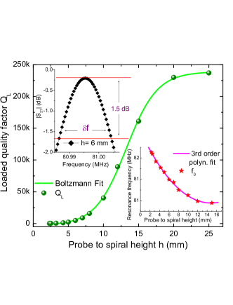
As seen from the figure, larger separation between magnetic loops leads to sharper transmission peaks, and consequently to a higher loaded quality factor, , which is calculated as [21] = /, where is the frequency at which the peak is located (i.e. resonance frequency) and is the bandwidth where is 1.5 dB below its peak value (see the top-left inset of Fig. 5). The loaded quality factor of the transmission data taken for = 3.25 mm is 1502 and for = 13.5 mm one finds 7800. These quality factor values are up to several orders of magnitude larger than their normal metal counterparts [17]. This brings up a discussion of the effect of coupling between the RF probes on the transmission data.
IV-B Coupling Between RF magnetic Loops
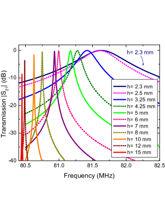
The measured is determined by external and internal loss factors and can be written as = / where is the stored energy in the spiral on resonance, is the resonant angular frequency and is the total dissipated power [23]. is the sum of power dissipated in the cavity (Ohmic losses), radiated power, and power leaking out of the spiral through the coupling loops. Since the measurements are done well below , ohmic and dielectric losses should be the smallest sources of dissipation. We find that the largest dissipation is due to the coupling losses from the RF loop probes. To confirm this, we have simulated the transmission curves numerically on a lossless single spiral of = 6 mm having the same dimensions as those used in the experiments shown in Fig. 3, utilizing the High Frequency Structure Simulator (HFSS) [22]. As seen in Fig. 4, shifts to lower frequencies with increasing , which is consistent with the data in Fig. 3, and the expectation from electromagnetic perturbation theory for a dominantly magnetic perturbation [24].
The loaded quality factor is observed to increase substantially as increases. This is consistent with an increase in the coupling quality factor, with weaker coupling, and = . A sigmoidal trend of is shown in Fig. 5 along with the polynomial decrease in with increasing .
V Towards Creation of an Artificial RF Medium: 1-D Arrays of the Spirals
V-A Linear Transmission Data below and above
So far, the discussion has been focused on a single element of the artificial medium, namely a single spiral showing a sub-100 MHz resonance. The metamaterial properties should be confirmed by examining an ordered collection of these elements.
The excitation of the linear array is as follows; the top loop is aligned with the first spiral of the array whereas the bottom loop is aligned with the last spiral. The distance between the edges of two spirals in the array is 1.5 mm, and is 3.25 mm. The measured transmission spectrum on a 1-D array of 7 spirals with = 6 mm, N = 40, = = 10 m is shown in the main panel of Fig. 6. The Nb spiral array is excited by an input power of 0 dBm at = 4.5 K, consequently multiple resonant peaks are observed which dissapear above the superconducting phase transition at . The inset of Fig. 6 shows the calculated transmission spectrum on the same spiral array, and gives resonant features at a slightly higher frequency (HFSS does not include or internal losses in the calculation).
V-B RF Power Evolution of Transmission Data and Nonlinearity
In the linear regime, the behavior of transmission data does not show any significant changes with respect to RF power put into the spiral cavity. The superconducting phase is strong and RF oscillations are maintained without significant Ohmic losses (the spiral can be modeled as an ideal inductor-capacitor (L-C) resonant circuit). As RF power is ramped up, the magnetic field starts to penetrate the spiral, particularly at weak spots in the superconducting film [19]. For higher RF input power, the dissipation caused by both vortex dynamics and Joule heating degrades superconductivity and introduces a resistance into the lumped element circuit analogue, and leads to nonlinear resonant features in the transmission data [25].
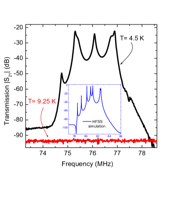
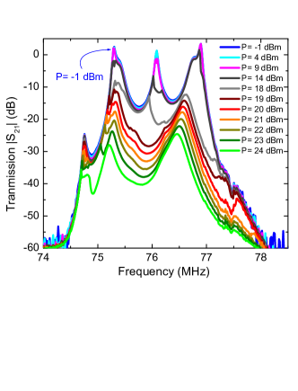
Fig. 7 shows the measured transmission data on the same 1-D array in Fig. 6 for a set of RF input powers, at a fixed ambient temperature of 4.2 K. At = -1 dBm, the resonance peaks are sharp and have high (linear case). With increasing input power dissipative processes nucleate at discrete sites in the spiral and increase the resistance of the circuit, which yields nonlinear resonant features in the transmission spectrum.
VI Conclusion
The linear and non-linear transmission characteristics of compact RF metamaterials employing Nb thin films are reported. In these RF metamaterials, the ohmic and dielectric losses are minimized by carrying out the experiments below the of Nb. The 2-D design simplifies the fabrication and maintains the uniformity of the artificial constituent elements. The robust magnetic response of the spirals can be sensitively tuned by manipulating the superconducting phase either with temperature or RF magnetic field. The resonant features in the spectra have an extremely high (compared to those of alternative normal metal metamaterials), making them promising for RF applications.
References
- [1] D. R. Smith, J. B. Pendry, and M. C. K. Wiltshire, “Metamaterials and Negative Refractive Index,” Science, vol. 305, pp. 788-792, Aug. 2004.
- [2] R. A. Shelby, D. R. Smith, and S. Schultz, “Experimental Verification of a Negative Index of Refraction,” Science, vol. 292, pp. 77-79, Apr. 2001.
- [3] M. C. K. Wiltshire, J. B. Pendry, W. Williams, J. V. Hajnal, “An effective medium description of Swiss Rolls a magnetic metamaterial,” J. Phys: Cond. Matt., vol. 19, p. 456216, Oct. 2007.
- [4] J. B. Pendry, A. J. Holden, D. J. Robbins, and W. J. Stewart, “Magnetism from Conductors and Enhanced Nonlinear Phenomena,” IEEE Trans. Microwave Theory Tech., vol. 47, no. 11, pp. 2075-2084, Nov. 1999.
- [5] Hou-Tong Chen, Willie J. Padilla, Joshua M. O. Zide, Arthur C. Gossard, Antoinette J. Taylor, Richard D. Averitt, “Active terahertz metamaterial devices,” Nature, vol. 344, pp. 597-600, Oct. 2006.
- [6] M. Wiltshire, “Radio frequency (RF) metamaterials,” Phys. Stat. Sol. B, vol. 244, no. 4, pp. 1227-1236, 2007.
- [7] M. C. K. Wiltshire, J. B. Pendry, I. R. Young, D. J. Larkman, D. J. Gilderdale, and J. V. Hajnal, “Microstructured Magnetic Materials for RF Flux Guides in Magnetic Resonance Imaging,” Science, vol. 291, p. 849, Feb. 2001.
- [8] M. J. Freire, R. Marques, “Planar magneto-inductive lens for three-dimensional subwavelength imaging,” Appl. Phys. Lett., vol. 86, p. 182505, 2005.
- [9] R. W. Ziolkowski and A. Erentok, “Metamaterial-Based Efficient Electrically Small Antennas,” IEEE Trans. Antennas Propag., vol. 54, pp. 2113-2130, July 2006.
- [10] N. Engheta, “An Idea for Thin Subwavelength Cavity Resonators Using Metamaterials With Negative Permittivity and Permeability,” IEEE Antennas Wirel. Propag. Lett., vol. 1, p. 10, 2002.
- [11] J. D. Baena, R. Marques, F. Medina, “Artificial magnetic metamaterial design by using spiral resonators,” Phys. Rev. B, vol. 69, p. 014402, Jan. 2004.
- [12] S. Massaoudi and I. Huynen, “Multiple Resonances in Arrays of Spiral Resonators Designed for Magnetic Resonance Imaging,” Microwave Opt. Technol. Lett., vol. 50, no. 7, pp. 1945-1950, Jul. 2008.
- [13] F. Bilotti, A. Toscano, L. Vegni, “Design of Spiral and Multiple Split-Ring Resonators for the Realization of Miniaturized Metamaterial Samples,” IEEE Trans. Antennas Propag., vol. 55, pp. 2258-2267, Aug. 2007.
- [14] S. S. Mohan, M. M. Hershenson, S. P. Boyd, and T. H. Lee, “Simple Accurate Expressions for Planar Spiral Inductances,” IEEE J. Solid-State Circuits, vol. 34, no. 10, pp. 1419-1424, Oct. 1999.
- [15] Z. Jiang, P. S. Excell, and Z. M. Hejazi, “Calculation of Distributed Capacitances of Spiral Resonators,” IEEE Trans. Microwave Theory Tech., vol. 45, pp. 139-142, Jan. 1997.
- [16] T. P. Orlando, K. A. Delin, Foundations of Applied Superconductivity, Burlington, MA: Addison-Wesley, 1991.
- [17] C. Kurter, J. Abrahams, S. M. Anlage, “Miniaturized superconducting metamaterials for radio frequencies,” Appl. Phys. Lett., vol. 96, p. 253504, Jun. 2010.
- [18] Quantum Design Physical Property Measurement System Resistivity Manual, Quantum Design Inc., San Diego, CA, 1999.
- [19] M. C. Ricci, H. Xu, R. Prozorov, A. P. Zhuravel, A. V. Ustinov, and S. M. Anlage, “Tunability of Superconducting Metamaterials,” IEEE Trans. Appl. Supercond., vol. 17, pp. 918-921, Jun. 2007.
- [20] A. P. Zhuravel, A. G. Sivakov, O. G. Turutanov, A. N. Omelyanchouk, S. M. Anlage, A. V. Ustinov,“Laser Scanning Microscope for HTS Films and Devices,” Low Temp. Phys., vol. 32, p. 592, Jun. 2006.
- [21] P. J. Petersan, S. M. Anlage, “Measurement of resonant frequency and quality factor of microwave resonators: Comparison of methods,” J. Appl. Phys., vol. 84, no. 6, pp. 3392-3402, Sep. 1998.
- [22] User’s Guide- High Frequency Structure Simulator, Ansoft Corporation, Pittsburgh, PA, 2005.
- [23] H. Padamsee, J. Knobloch, T. Hays, RF Superconductivity for Accelerators, 2nd ed. Weinheim: Wiley-VCH, 2008.
- [24] S. Ramo, J. R. Whinnery, T. Van Duzer, Fields and Waves in Communication Electronics, New York: Wiley-VCH, 1984, p. 512.
- [25] B. Abdo, E. Segev, O. Shtempluck, E. Buks, “Nonlinear dynamics in the resonance line shape of NbN superconducting resonators,” Phys. Rev. B, vol. 73, p. 134513, Apr. 2006.