Trapping-detrapping fluctuations in organic space-charge layers
Abstract
A trapping-detrapping model is proposed for explaining the current fluctuation behavior in organic semiconductors (polyacenes) operating under current-injection conditions. The fraction of ionized traps obtained from the current-voltage characteristics, is related to the relative current noise spectral density at the trap-filling transition. The agreement between theory and experiments validates the model and provides an estimate of the concentration and energy level of deep traps.
Polymeric as well as small molecular semiconductor electronic products have shown impressive improvements in their performance during recent years. Organic field-effect transistors (OFETs) and light-emitting diodes (OLEDs), solar cells and memories successfully compete with traditional electronic devices when flexibility, large area, low cost and weight are the main requirements Muccini ; Fleissner ; Chen . The injection of charge carriers at molecule-metal interfaces plays a decisive role in the performance of organic semiconductor devices. Defect states drastically alter the injection mechanism, hence their origin and effect on charge transfer across the interface is one of the main investigation issues. Charge carrier trapping-detrapping processes have been indeed recognized as source of current instability and degradation of organic FETs Lang ; Miyadera ; Koch ; Yang ; Knipp ; Dinelli ; Schwalb ; Deboer ; Kang ; Chandra ; Giulianini .
Current and voltage noise have been widely exploited as a spectroscopic tool for investigating the role of deep defect states in inorganic insulators and wide-bang gap semiconductors operating under current-injection conditions Kleinpenning ; Vanvliet ; Pennetta ; Verleg ; Mazzetti ; Tsormpatzoglou . A comparatively smaller number of works have been addressed to noise in organic devices Carbone05 ; Jurchescu ; SampietroNecliudovMartin . Relative current spectral densities obtained on polyacenes have evidenced a striking peaked behavior at voltages corresponding to the trap filling transition (TFT) between Ohmic () and Space Charge Limited Current (SCLC) regimes. This behavior has been interpreted as evidence for continuous percolation between the two regimes, considered as different electronic phases. Accordingly, at the TFT, the clustering of insulating regions should lead to a reduction of the ohmic paths. The overall effect was expected to give a substantial increase of noise in analogy with the increasing of fluctuations near a structural phase transition Carbone05 . However, a comprehensive quantitative investigation of noise behavior in organic materials is still lacking.
Here, we present a complementary interpretation based on trapping-detrapping processes of injected carriers at the TFT. Accordingly, we carry out a quantitative comparison between theory and experiments, for both transport and noise. The trap filling transition takes place in the range of voltages , with the threshold value for the onset of TFT and a constant whose value depends on the steepness of the transition. These voltage values correspond to the energy range where the quasi-Fermi level crosses the trap level. In Kleinpenning , the relative-noise crossover between Ohmic and SCLC regimes was investigated in the absence of TFT in silicon. Here, that model is generalized by accounting for the presence of the trap-filling region between the Ohmic and SCLC regimes. For a two terminal sample of length and cross-sectional area , the expressions of the current-voltage (-) characteristics and the spectral density of voltage fluctuations can be written as follows.
1. Ohmic regime:
| (1a) | |||||
| (1b) | |||||
where is the elementary charge, the density and the mobility of free thermal carriers, the frequency and the Ohmic Hooge parameter. The relative noise power spectral density is:
| (2) |
Eq. (2) implies that the relative noise is constant in the Ohmic regime as voltage increases.
2. SCLC regime:
| (3a) | |||||
| (3b) | |||||
where and are, respectively, the relative dielectric constant of the material and the vacuum permittivity, the SCLC Hooge parameter. The product appearing in Eq. (3a) is usually referred to as effective mobility with given by:
| (4) |
where and are respectively the free and trapped carrier density, is the trap degeneracy factor, the density of states in the valence band (for -type transport the density of states in the conduction band should be considered), the trap energy level, the thermal energy. The relative noise power spectral density is:
| (5) |
Equation (5) implies that the relative noise decreases as in the SCLC regime as voltage increases.
3. TFT regime:
To the purpose of describing the noise at the TFT region, we consider the trapping-detrapping processes as the main source of fluctuations.
Following the standard approach within a linear kinetics of trapping processes Vanvliet , the variance of the total number of ionized traps is where is total number of traps in the volume of the device. Hence, the relative noise power spectrum writes:
| (6) |
where is the carrier free time and the fraction of ionized traps. Accordingly, is a function of the applied voltage through the position of the quasi-Fermi level with respect to the trap energy level. It is worth noting that vanishes at the extremes of the TFT and reaches the maximum value at , corresponding to half the filling of the total number of traps. The total relative current noise as function of the applied voltage is then given by the sum of three independent contributions as follows:
| (7) |
where is given by the Mark-Helfrich law mark62 :
| (8) |
Equation (7) is the major assumption of the present model and is applied to the case of tetracene. To this purpose, the function is obtained by fitting the - characteristics and then introduced in Eq. (6) as described below. The total current is written as sum of an Ohmic and an SCLC current generator Giulianini . In correspondence of the TFT regime the relative weight of the two current generators depends on the applied bias through the fraction of filled traps :
| (9) |
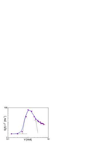
For the validation of the model, we refer to the set of experiments carried out on polyacenes purified by sublimation, evaporated on glass at Pa and room temperature. Sandwich structures with Au, Al and ITO electrodes (namely Au/Pc/ITO, Au/Tc/Al, Au/Pc/Al) with area , distant with , have been characterized. This large sample set ensures a reliable statistics over the wide variability of chemical and structural properties. Results of - and for a tetracene thin film of length and cross-sectional area are shown. From the values of the Ohmic and SCLC region of - characteristics, using Eq. (1a), Eq. (3a) and , we find and . From the SCLC region of the - characteristics, the effective mobility is obtained. From the Ohmic region of the - characteristics, is obtained. Since an independent determination of the Ohmic mobility is not available, we assume that ranges between , which are reasonable values for low and high quality crystalline materials. Accordingly, by keeping the same level of fit, the values of the parameters related to the mobility can take values in the range and . By using Eq. (4) with , , it is . The values of the function obtained from the fit of the - characteristics (see Fig. 1) are then introduced in Eq. (6) to reproduce the noise behavior at the trap-filling transition. Figure 2 shows the experimental relative current spectral density (circles) and its decomposition in terms of Eq. (7) (dashed lines). The quantity , fitting the total excess noise in the TFT regime, is given by s, where is the maximum value of the relative noise. The maximum value of trap concentration compatible with the model used for fitting is . For this value the carrier free time is . The range of parameter values obtained from the fit are summarized in Table 1. As illustrated by Figs. 1 and 2, the theory reproduces quite well both transport and noise behavior at the trap-filling transition. Furthermore, the values of the parameters are compatible with those reported in the literature Deboer . By taking the values of the power spectral density at , we find and . We remark that the Hooge parameter differs from to account for the difference in the tetracene medium when going from Ohmic (neutral traps) to SCLC (charged traps) conditions. These values are low when compared with the typical values of about in most crystalline semiconductors. These low values can be ascribed to the fact that transport takes place in insulators via a microscopic mechanism of hopping type.
In conclusion, by introducing a trapping-detrapping noise contribution associated with the presence of a TFT regime, we have developed a microscopic model which provides a quantitative interpretation of the current voltage and relative current noise in tetracene as function of the applied voltage. The noise mechanism in the TFT region is basically related to the fluctuating occupancy of a single level of traps, which modulates the cross-section of the conducting channels and, thus, produces noise. The consistent fit of transport and noise provides a set of parameters (see Table 1) of valuable interest for the characterization of the material. We remark that the measured current noise spectrum was found to be more likely to an -sloped rather than Lorentzian, thus, the lifetime estimate should be taken as rather indicative. The broadening of the trap level energy could account for such a spectral difference Vanvliet ; Pennetta . Finally, we note that the proposed model can be generalized to the case of several trap levels and hopping transport.
Acknowledgements.
The support of D. Kotowski, B. Kutrezba-Kotowska and M. Tizzoni is gratefully acknowledged.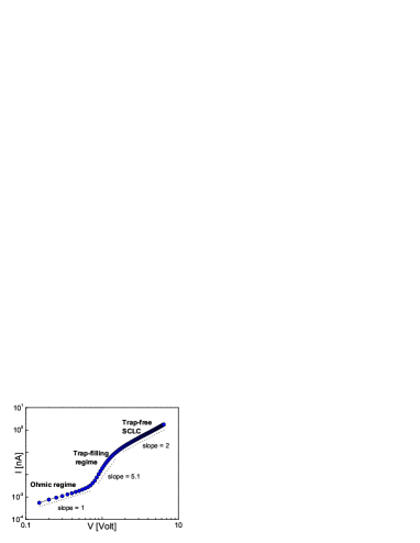
| Density of traps | ||
|---|---|---|
| Valence band state density | ||
| Carrier free time | ||
| Zero-field hole mobility | ||
| Deep trap energy level | ||
| Effective mobility parameter | ||
| Thermal free carrier concentration | ||
| Ohmic Hooge parameter | ) | |
| SCLC Hooge parameter |
References
- (1) M. Muccini, Nature Materials 5, 605 (2006).
- (2) A. Fleissner et al. Appl. Phys. Lett. 91, 242103 (2007).
- (3) C.Y. Chen et al. Appl. Phys. Lett. 93, 223301 (2008).
- (4) D.V. Lang et al. Phys. Rev. Lett. 93, 076601 (2004).
- (5) T. Miyadera et al. Appl. Phys. Lett. 93, 033304 (2008).
- (6) N. Koch et al. Appl. Surf. Sc. 244, 593, (2005).
- (7) Y.S. Yang et al. Appl. Phys. Lett. 80, 1595 (2002).
- (8) D. Knipp, R.A. Street, and A.R. Volkel, Appl. Phys. Lett. 82, 3907 (2003).
- (9) F. Dinelli et al. Phys. Rev. Lett. 92, 116802 (2004).
- (10) C.H. Schwalb et al. Phys. Rev. Lett. 101, 146801 (2008).
- (11) R.W.I. De Boer et al. J. Appl. Phys. 95, 1196 (2004).
- (12) J.H. Kang et al. Appl. Phys. Lett. 86, 152115 (2005).
- (13) W. Chandra et al. Appl. Phys. Lett. 90, 153505 (2007).
- (14) M. Giulianini et al. Appl. Phys. Lett. 94, 083302 (2009); I. Torres, D.M. Taylor, E. Itoh Appl. Phys. Lett. 85, 314-316 (2004).
- (15) T.G.M. Kleinpenning, Physica B,C 94, 141 (1978); F.N. Hooge, T.G.M. Kleinpenning, and L.K.J. Vandamme, Rep. Prog. Phys. 44, 479 (1981).
- (16) C.M. Van Vliet, J. Appl. Phys. 93, 6068 (2003).
- (17) C. Pennetta, E. Alfinito, L. Reggiani, J. Stat. Mech., P02053 (2009).
- (18) P. Verleg, J.I. Dijkhuis Phys. Rev. B 58, 3904 (1998).
- (19) A. Carbone, P. Mazzetti, J. Appl. Phys. 80 1559 (1996); Phys. Rev. B 49 7592 (1994).
- (20) A. Tsormpatzoglou et al. J. Appl. Phys. 100, 074313 (2006).
- (21) A. Carbone, B.K. Kotowska and D. Kotowski, Phys. Rev. Lett. 95, 236601 (2005); Eur. Phys. J. B50, 77 (2006).
- (22) O.D. Jurchescu et al. Appl. Phys. Lett. 92, 132103 (2008).
- (23) S. Martinet et al., J. Appl. Phys. 88, 5395 (2000); P. V. Necliudov, et al. J. Appl. Phys. 87, 3381 (2000); M. Sampietro et al. Appl. Phys. Lett. 78, 3262 (2001).
- (24) P. Mark and W. Helfrich. J. Appl. Phys. 33, 205, (1962).