Gate-controlled conductance through bilayer graphene ribbons
Abstract
We study the conductance of a biased bilayer graphene flake with monolayer nanoribbon contacts. We find that the transmission through the bilayer ribbon strongly depends on the applied bias between the two layers and on the relative position of the monolayer contacts. Besides the opening of an energy gap on the bilayer, the bias allows to tune the electronic density on the bilayer flake, making possible the control of the electronic transmission by an external parameter.
pacs:
61.46.-w, 73.22.-f, 73.63.-bThe prospective use of graphene in nanoelectronics requires the possibility to open gaps in its band structure in a controllable way. Due to the chiral nature of the carriers Castro-Neto et al. (2009), it is not easy to open gaps and confine carriers in a single graphene monolayer. Carbon-based structures as nanoribbons Nakada et al. (1996); Brey and Fertig (2006), nanotubes Chico et al. (1996, 1998); Santos et al. (2009), and graphene bilayers Nilsson et al. (2007); Castro et al. (2007); Snyman and Beenakker (2007); Oostinga et al. (2007); Fiori and Iannaccone (2009); Russo et al. (2009) are viable materials for nanoelectronics, since it is feasible to change their electronic characteristics from semiconducting to metallic as a function of geometric or external parameters. Bilayer graphene is a good candidate because a gap can be opened and controlled by an applied bias between its two layers. Monolayer graphene nanoribbons (MGNs) stand out as optimal electrodes for systems based on bilayer graphene, with the aim of achieving the best integration of nanoelectronic components. Thus, it is important to study the electronic transport of bilayer graphene nanoribbons (BGNs) with MGN contacts. Previous work has focused on the electronic transport through bilayer graphene flakes in absence of external gates González et al. (2010). In such a case the conductance shows strong oscillations as a function of the energy of the incident electron and the length of the bilayer region. In this work we show that the conductance of BGNs connected to MGNs strongly depends on the way the bilayer is contacted and on the applied gate voltage. This allows for an external control of the electronic properties of the system.
Geometry. We analyze electronic transport in the linear regime through a gated BGN connected to two metallic MGN contacts. The monolayer leads can be either armchair or zigzag graphene nanoribbons Nakada et al. (1996); Brey and Fertig (2006), serving as contacts to armchair or zigzag bilayer flakes respectively. In both cases two configurations are possible: the bottom-bottom (11) and the bottom-top (1), where the ribbon leads are connected to the same (11) or to a different monolayer (1) of the bilayer flake. We consider BGN of width and length , and restrict our study to narrow nanoribbons in the energy range for which only one incident electron channel is active. The bias is applied symmetrically with respect to the top () and the bottom () layers.
Electronic structure of constituents. The band structure of graphene has two inequivalent valleys. Within one valley, the low energy properties of graphene are well described by the two dimensional Dirac equation, , where m/s is the Fermi velocity, is the momentum operator relative to the Dirac point and are the Pauli matrices. The Dirac Hamiltonian acts on a two-component spinor, , representing the amplitude of the wavefunction on the two inequivalent triangular sublattices of graphene, labeled and . The band structure of armchair graphene nanoribbons is obtained from the Dirac equation with the appropriate boundary conditions Brey and Fertig (2006). In all nanoribbons the transverse momentum is quantized. For the armchair MGN case, when the number of carbon atoms across the width of the ribbon is equal to , being a positive integer, the smallest transverse momentum is zero. This yields the ribbon metallic with an energy dispersion , where is the momentum along the nanoribbon.
In addition to confined states, zigzag MGNs support zero energy surface states located at the edges of the ribbon Nakada et al. (1996). In reciprocal space, surface states occur between the two Dirac cones and their number cannot be described by the two dimensional Dirac equation, which is only valid for the low energy physics near the cones. Therefore, to describe zigzag graphene nanoribbons we use a nearest-neighbor tight-binding Hamiltonian . Here annihilates an electron on site of sublattice , and the hopping parameter is related to the Fermi velocity by , where is the graphene lattice constant, Å.
Bilayer graphene consists of two coupled graphene layers with inequivalent sites and on the bottom and top layers respectively. We consider the Bernal stacking in which the sublattice is exactly on top of the sublattice . Within one valley, the low energy properties of a biased bilayer graphene are well described McCann and Fal’ko (2006) by the Hamiltonian
| (1) |
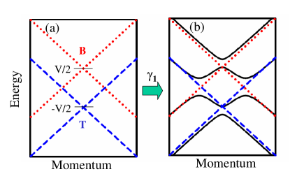
where is the hopping parameter between the closest carbon atoms belonging to different layers, are again the Pauli matrices for the sublattice degree of freedom and are the Pauli matrices for the layer index ( and are the unit matrices in both subspaces). This Hamiltonian acts on the four-component spinor representing the amplitude of the wavefunction on the two sublattices and of the two layers and . The energy bands are . The low energy band has a Mexican hat shape with a minimum gap , see Fig. 1. The minimum gap of the second subband is and occurs at . Fig. 1 illustrates how the Mexican hat shape and the split-off bands arise: without interlayer hopping, the applied bias shifts the linear band dispersions of the two layers; the interaction between layers opens gaps at the intersections of the bands.
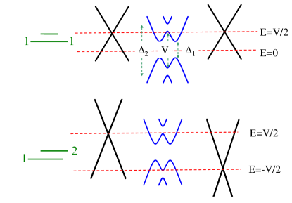
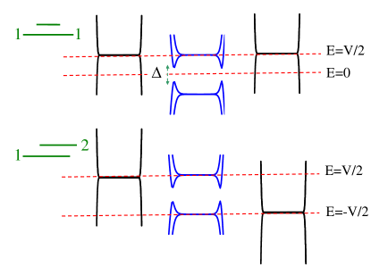
The electronic structure of an armchair BGN depends on the width of the ribbon. As in the monolayer case, when the number of carbon atoms along a BGN layer is equal to , the smallest transverse momentum is zero, and the dispersion of the armchair BGN is , being the momentum along the ribbon, see Fig. 2. In the case of zigzag biased BGNs the system supports two kinds of surface states Castro et al. (2008): (i) states with energies , similar to those occurring in zigzag MGNs, and (ii) valley-polarized states with energies in the gap. At each edge of the ribbon there are two surface states carrying current in opposite directions and belonging to different valleys. These states have a topological nature Martin et al. (2008) but the metallicity of the edge is not protected against intervalley scattering nor against interedge intravalley scattering. The latter occurs when the ribbon width is smaller than the penetration length of the surface states A.Morpurgo , , that for realistic values of the interlayer hopping is around 17. This large value produces an interedge scattering gap in the spectrum of narrow zigzag BGNs, see Fig. 3. Although the valley-polarized surface states can be modeled with the Dirac Hamiltonian, the coupling between states localized in opposite edges is better described using a tight-binding Hamiltonian, which takes into account the coupling between inequivalent Dirac points.
Electronic conductance. Armchair nanoribbons. As discussed above, the Dirac Hamiltonian describes appropriately the low energy band structure of armchair nanoribbons. Therefore, we calculate the conductance of the system by matching the eigenfunctions of the Dirac-like Hamiltonian. Given an incident electron coming from the left monolayer ribbon and with energy , we compute the transmission coefficient to the right monolayer lead. The boundary conditions on the wavefunctions determine the value of the transmission. In the bottom-bottom configuration (11) the wavefunctions of the bottom layer and should be continuous at the beginning () and at the end () of the bilayer region. For the top layer the wavefunction should vanish in one sublattice at and on the other sublattice at , e.g., . In the bottom-top configuration the bottom wavefunctions and the top wavefunctions should be continuous at and respectively. In addition, the hard-wall condition should be satisfied, . Zigzag nanoribbons. To describe adequately the low energy properties of zigzag nanoribbons in the full Brillouin zone it is necessary to use a tight-binding Hamiltonian. We use a Green’s function approach to obtain the transport properties Chico et al. (1996); Datta (1995); González et al. (2009). In this method the system is divided in three parts, namely, a finite-size bilayer section connected to the right and left monolayer semi-infinite leads. The Green’s function of the central region is
| (2) |
where is the bilayer Hamiltonian and and are the selfenergies at the ends of the bilayer region due to the presence of the leads. The selfenergies contain the information on the type of connection, i.e., 11 or 12, of the system. In the linear regime, the conductance is given by
| (3) |
where is the transmission at the Fermi energy and and are the couplings between the bilayer and the left and right monolayer leads respectively.
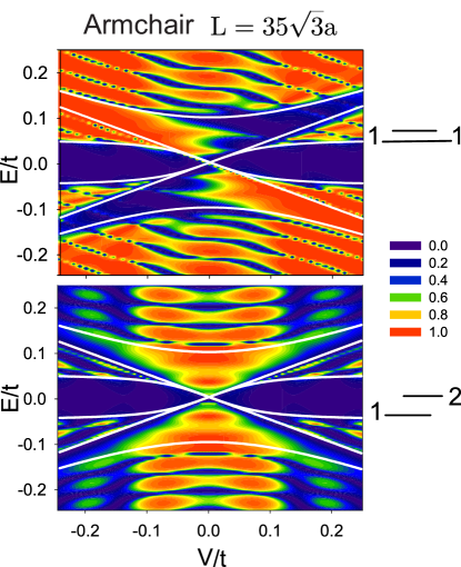
Results. Armchair nanoribbons. In Fig. 4 we plot the transmission as a function of the incident energy and the applied gate voltage for an armchair nanoribbon system in the 11 and 12 configurations. The length of the bilayer flake is and the value of the interlayer hopping is . The results are independent of the width of the ribbon, provided that the monolayer ribbons are metallic and that the energy of the incident electron is lower that the energy of the second subband. The transmission is obtained in the continuum approximation, but we have checked that the results coincide with those obtained within the tight-binding approach. Due to the symmetry of the contacts, the 12 configuration shows electron-hole and symmetry. This is not the case for the 11 configuration, for which the location of the contacts precludes those symmetries. In both cases the conductance is suppressed for energies in the gap , for which there are no available states for the conductance in the bilayer region. We first discuss the results for the bottom-bottom configuration. In the energy window there are two propagating states in the bilayer part and the conductance is finite. In the range of energies there is only one propagating mode in the central region; but in this configuration, when and have the same sign, this mode is mostly located in the opposite (top) layer to the leads (bottom), as can be seen in Fig. 1(b), and the conductance is near zero. Thus, by applying a gate voltage between the two layers we can tune the electronic density in the bilayer. Changing the distribution of carriers from one layer to the other allows to control the conductance of the system by means of an external parameter. For energies the transmission is finite with antiresonances associated with interferences in the bilayer region due to the existence of two propagating channels. González et al. (2010) These interferences are weaker for voltages , with and overall nonzero conductance, because in this case the incident current from the left electrode is transmitted efficiently to the upper branch of the bilayer dispersion relation, with bottom character, and from there to the right (bottom) lead, with an almost perfect wavevector matching Chico and Jaskólski (2004). The weak interferences are due to the bilayer-confined states arising from the coupling to the top layer flake. Note the linear dependence of the position of the antiresonances on the applied voltage: the energy of the confined states in the top layer are displaced by the applied bias , thus changing the occurence of the antiresonances correspondingly.
In the bottom-top configuration the conductance is not suppressed for because in this case the incoming and outgoing electrons belong to different layers: the propagating mode in the bilayer has a predominant top character (see Fig. 1), being easily transmitted to the right electrode. For this configuration, the transmission at energies is generally suppressed, even though there are two propagating modes in the bilayer. This can be understood by noticing the wavevector mismatch Chico and Jaskólski (2004) between left and right electrodes produced by the applied bias, as depicted in Fig. 1. Away from the gap the transmissions in the 11 and 12 configurations are rather complementary; the antiresonances that occur in the 11 configuration become resonances in the 12 case. This complementarity of the conductance can be understood by resorting to a simple non-chiral model. Consider an incident carrier, with energy larger than the gap, coming from the left and therefore in the bottom sheet. When arriving at the bilayer central region, the incident wavefunction decomposes into a combination of the two eigenstates of the biased bilayer. The conductance through the bilayer region is proportional to the probability of finding an electron at the top (bottom) end of the central region for the bottom-top (bottom-bottom) configuration. As the total probability of finding the electron at the end of the bilayer region is unity, the bottom-bottom and the bottom-top transmissions should be the opposite.
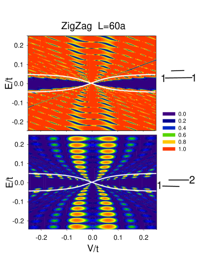
Zigzag nanoribbons. In Fig.5 we plot the transmission as function of the Fermi energy and the applied gate voltage for zigzag nanoribbons in the 11 and 12 configurations. These results have been obtained using a tight binding Hamiltonian and a recursive Green’s function technique Chico et al. (1996); Datta (1995); González et al. (2009). The conductance of zigzag graphene nanoribbons depends on the ribbon width. The results presented in Fig.5 correspond to a narrow ribbon, , for which there is only one channel coming from the left contact for all the plotted energies. As for the armchair-based systems, there is a strong complementarity between the 11 and the 12 configurations, yielding a very different conductance as a function of the energy and bias for the two configurations. Other features, as antiresonances (resonances) in the bottom-bottom (bottom-top) configuration are similar to those occurring in armchair nanoribbons and have the same origin. In the upper panel of Fig. 5, corresponding to the 11 configuration, the previous gapped region in the armchair case between and has shrunk to a line of slope . This is easy to understand by observing the zigzag bandstructure of Fig. 3. Another remarkable feature in Fig. 5 is the existence of a transport gap smaller than the bulk gap of the gated bilayer. As mentioned above, the gap appears because of the coupling between states with the same valley polarization localized in different edges and moving in opposite directions. The penetration length of these surface states is rather large; for nanoribbons narrower than this produces a noticeable transport gap smaller than the bulk gap.
In summary, we have calculated the conductance of bilayer graphene flakes with monolayer nanoribbon contacts with a bias voltage between layers. Depending on the position of the electrodes and on the applied bias, there is a strong variation of the conductance. Besides the energy gap opened by the bias, the conductance can be tuned by changing the spatial distribution of the carriers in the bilayer region, thus allowing for the external control of the transport through graphene bilayer flakes.
Acknowledgments. This work has been partially supported by MEC-Spain under grant FIS2009-08744. J.W.G. would like to gratefully acknowledge helpful discussions with Dr. L. Rosales, the ICMM-CSIC for their hospitality and the financial support of MESEUP research internship program, CONICYT (CENAVA, grant ACT27) and USM 110856 internal grant.
References
- Castro-Neto et al. (2009) A. H. Castro-Neto, F.Guinea, N.M.R.Peres, K.S.Novoselov, and A.K.Geim, Rev. Mod. Phys. 81, 109 (2009).
- Nakada et al. (1996) K. Nakada, M. Fujita, G. Dresselhaus, and M. S. Dresselhaus, Phys. Rev. B 54, 17954 (1996).
- Brey and Fertig (2006) L. Brey and H. Fertig, Phys. Rev. B 73, 195408 (2006).
- Chico et al. (1996) L. Chico, L. X. Benedict, S. G. Louie, and M. L. Cohen, Phys. Rev. B 54, 2600 (1996).
- Chico et al. (1998) L. Chico, M. P. López-Sancho, and M. Muñoz, Phys. Rev. Lett. 81, 1278 (1998).
- Santos et al. (2009) H. Santos, L. Chico, and L. Brey, Phys. Rev. Lett. 103, 086801 (2009).
- Nilsson et al. (2007) J. Nilsson, A. H. Castro Neto, F. Guinea, and N. M. R. Peres, Phys. Rev. B 76, 165416 (2007).
- Castro et al. (2007) E. V. Castro, K. S. Novoselov, S. V. Morozov, N. M. R. Peres, J. M. B. L. dos Santos, J. Nilsson, F. Guinea, A. K. Geim, and A. H. C. Neto, Phys. Rev. Lett. 99, 216802 (2007).
- Snyman and Beenakker (2007) I. Snyman and C. W. J. Beenakker, Phys. Rev. B 75, 045322 (2007).
- Oostinga et al. (2007) J. B. Oostinga, H. B. Heersche, X. Liu, A. F. Morpurgo, and L. M. K. Vandersypen, Nature Materials 7, 151 (2007).
- Fiori and Iannaccone (2009) G. Fiori and G. Iannaccone, Electron Device Letters, IEEE 30, 261 (2009).
- Russo et al. (2009) S. Russo, M. Craciun, M. Yamamoto, S. Tarucha, and A. Morpurgo, New J.Phys. 11, 095018 (2009).
- González et al. (2010) J. W. González, H. Santos, M. Pacheco, L. Chico, and L. Brey, Phys. Rev. B 81, 195406 (2010).
- McCann and Fal’ko (2006) E. McCann and V. I. Fal’ko, Phys. Rev. Lett. 96, 086805 (2006).
- Castro et al. (2008) E. V. Castro, N. M. R. Peres, J. M. B. Lopes dos Santos, A. H. C. Neto, and F. Guinea, Phys. Rev. Lett. 100, 026802 (2008).
- Martin et al. (2008) I. Martin, Y. M. Blanter, and A. F. Morpurgo, Phys. Rev. Lett. 100, 036804 (2008).
- (17) A.Morpurgo, talk given at the Graphene Week 2010. April 2010, College Park, MD.
- Datta (1995) S. Datta, Electronic Transport in Mesoscopic Systems (Cambridge University Press, Cambridge, 1995).
- González et al. (2009) J. González, L. Rosales, and M. Pacheco, Physica B: Condensed Matter 404, 2773 (2009).
- Chico and Jaskólski (2004) L. Chico and W. Jaskólski, Phys. Rev. B 69, 085406 (2004).