Quantum-interference-controlled three-terminal molecular transistors based on a single ring-shaped-molecule connected to graphene nanoribbon electrodes
Abstract
We study all-carbon-hydrogen molecular transistors where zigzag graphene nanoribbons play the role of three metallic electrodes connected to a ring-shaped 18-annulene molecule. Using the nonequilibrium Green function formalism combined with density functional theory, recently extended to multiterminal devices, we show that the proposed nanostructures exhibit exponentially small transmission when the source and drain electrodes are attached in a configuration that ensures destructive interference of electron paths around the ring. The third electrode, functioning either as an attached infinite-impedance voltage probe or as an “air-bridge” top gate covering half of molecular ring, introduces dephasing that brings the transistor into the ‘on’ state with its transmission in the latter case approaching the maximum limit for a single conducting channel device. The current through the latter device can also be controlled in the far-from-equilibrium regime by applying a gate voltage.
pacs:
85.35.Ds, 85.65.+h, 73.63.Rt, 72.80.VpIntroduction.—The recent fabrication Wang2008a ; Cai2010 of graphene nanoribbons (GNRs) with ultrasmooth edges has opened unforeseen avenues for nanoelectronics Schwierz2010 by providing a novel type of semiconducting channel (GNRs with armchair edges of sub-10-nm width and band gaps eV) for field-effect transistors (FETs) Wang2008a or low-dissipation interconnects Areshkin2007a (metallic GNRs with zigzag edges). Furthermore, metallic GNRs have the capability to resolve one of the key challenges Kiguchi2008 for molecular electronics Cuniberti2005 —a well-defined molecule-electrode contact with high transparency, strong directionality and reproducibility.
This is due to the fact that strong molecule-GNR - coupling makes possible formation of a continuous -bonded network across GNR and orbitals of conjugated organic molecules Ke2007 . In addition, unusual electronic structure Areshkin2007a of zigzag GNRs (ZGNRs) and the possibility to control it via edge doping Cervantes-Codi2008 offer prospect for device designs that are outside of the scope of traditional approaches in molecular electronics where single molecules are in contact with metals Kiguchi2008 ; Song2009 , such as gold or platinum which suffer from the lack of directional covalent bonding thereby leading to poor reproducibility of most metal-molecule-metal junctions Stokbro2003 , or carbon nanotubes Guo2006 where edges are not present and which do not have planar structure appropriate for aligning and patterning through lithographic methods suitable for high-volume production.
Unlike carbon nanotubes (CNTs), which were employed experimentally Guo2006 as electrodes of molecular devices and whose contact to conjugated molecules has been investigated via first-principles quantum transport methods Ke2007 , surprisingly little is known about linear response or far-from-equilibrium transport properties of multiterminal molecule-GNR heterojunctions. Although pristine ZGNRs have a band gap at low temperature due to edge magnetic ordering Yazyev2008 ; Areshkin2009 , this gap is easily destroyed at room temperature Yazyev2008 or by defects and impurities along the edge Areshkin2009 ; Jiang2008 .
To obtain transistor effect, current through the molecular junction has to be controlled by the third electrode acting either as an electrostatically coupled gate Schwierz2010 in traditional FET designs Song2009 or as being attached to the molecule in quantum-interference-controlled transistor (QICT) concepts Cardamone2006 . In the recently proposed QICT, source and drain electrodes are connected to a ring-shaped molecule in a configuration that ensures destructive interference Nazarov2009 of electron paths around the ring and, therefore, ‘off’ state of QICT with perfect zero leakage current. The third electrode, acting as the so-called Büttiker voltage probe which does not draw any current Nazarov2009 , is then attached to the molecule to introduce dephasing and thereby ‘on’ state of QICT.
The QICT also offers a playground for basic research on quantum interference effects Nazarov2009 in molecular electronics which, unlike in conventional two-dimensional electron gases or graphene, can manifest itself even at room temperature since molecular vibrations with dephasing effect (i.e., those that change the length difference between paths around the ring) can be suppressed Cardamone2006 below 500 K. Such interference effects in transport through aromatic molecules have attracted considerable attention in the very recent experimental and theoretical studies Rincon2009 . Furthermore, potential applications of QICT involve operation with greatly reduced heat dissipation because the current flow is not blocked by an energy barrier as in traditional FETs where it must be raised and lowered with each switching cycle in either silicon-based or carbon-based FETs Schwierz2010 .

Understanding of realistic junctions of ZGNR and molecules requires quantum transport methods combined with the first-principles input about atomistic and electronic structure to capture charge transfer in equilibrium (which is indispensable to obtain correct linear response conductance of, e.g., carbon-hydrogen systems Areshkin2010 ) or charge redistribution (whose knowledge ensures the gauge invariance of the current-voltage characteristics) in the far-from-equilibrium regime driven by finite bias voltage. The state-of-the-art approach that can capture all of these effects, as long as the coupling between the molecule and the electrodes is strong enough to diminish Coulomb blockade effects Cuniberti2005 , is the nonequilibrium Green function formalism combined with density functional theory (NEGF-DFT) Cuniberti2005 ; Areshkin2010 . However, due to the lack of NEGF-DFT algorithms for multiterminal devices, previous efforts to model QICT based on benzene-gold Cardamone2006 ; Ke2008 , annulene-gold Ke2008 , benzene-CNT Ke2008 and annulene-CNT Ke2008 junctions have employed either semi-empirical models Cardamone2006 (with truncated basis set and the connection between the leads and the molecule treated phenomenologically, thereby ignoring possible structural relaxation or hybridization between molecular states and contact states) or NEGF-DFT Ke2008 but in the absence of third attached electrode.
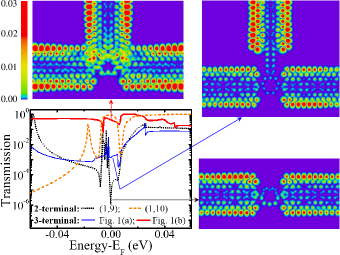
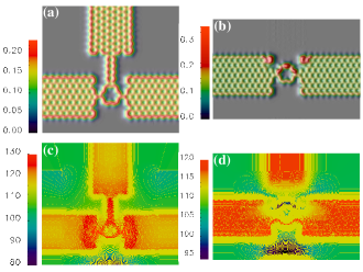
In this Letter, we analyze linear response and nonequilibrium transport properties of ZGNR18-annuleneZGNR junctions, whose third electrode is made of ZGNR as well, by employing the very recently developed NEGF-DFT formalism for multiterminal nanostructures (MT-NEGF-DFT) Saha2009a . The third electrode introduces dephasing by being attached to the molecule to act as an infinite-impedance voltage probe Nazarov2009 , as shown in Fig. 1(a). Moreover, we find an even larger disruption of destructive quantum interference in a setup proposed in Fig. 1(b) where the third electrode plays the role of a top gate covering the upper-half of annulene ring while being separated from the two terminal device underneath by an air gap. Our principal result is shown in Fig. 2 where exponentially small transmission between the source electrode 1 and the drain electrode 2 at the Fermi energy in the junction with destructive geometry for connecting the two ZGNR electrodes increases by three orders of magnitude with the attachment of an infinite-impedance voltage probe. Moreover, the junction becomes highly transparent due to induced states (Fig. 2) and charge transfer (Fig. 3) underneath the “air-bridge” top gate. We also analyze in Fig. 4 the gate voltage modulation of source-drain current in the far-from-equilibrium transport regime of device in Fig. 1(b).
Device setup and MT-NEGF-DFT formalism.—Although naïvely one would expect that formation of continuous -bonded network between carbon-based electrodes and conjugated molecules would ensure high contact transparency, early experiments Guo2006 on CNTmoleculeCNT heterojunctions have measured surprisingly small conductances for a variety of sandwiched molecules suggesting poor contact transparency. The first-principles analysis of different setups reveals that this is due to significant twisting forces when molecule is connected to CNT via, e.g., 6-membered rings Ke2007 . Therefore, to keep nearly parallel and in-plane configuration (hydrogen atoms of annulene slightly deviate from the molecular plane) of our ZGNR18-annuleneZGNR junction, we use a 5-membered ring Ke2007 in Fig. 1 to chemically bond ZGNR to annulene. The atomic structure of the heterojunctions in Fig. 1 is fully optimized by minimizing the atomic forces on individual atoms to be smaller than eV/Å. This preserves the overall conjugation and leads to strong coupling and high contact transparency, as confirmed by Fig. 2 where for ZGNR electrodes attached to annulene atoms (1,10) as an example of configuration with constructive quantum interference.
The high contact transparency also makes it possible to apply the NEGF-DFT framework, which would otherwise be rendered insufficient due to electronic correlations Darau2009 emerging in the weak coupling regime that are beyond the mean-field DFT treatment Cuniberti2005 . In the NEGF-DFT formalism, the Hamiltonian is not known in advance and has to be computed by finding converged charge redistribution via the self-consistent DFT loop for the density matrix whose trace gives the charge density Cuniberti2005 ; Areshkin2010 . The NEGF formalism for steady-state transport operates with two central quantities, retarded and lesser Green functions, which describe the density of available quantum states and how electrons occupy those states, respectively. The technical details of the construction of the nonequilibrium density matrix for multiterminal devices are discussed in Ref. Saha2009a . In Fig. 3, we show the equilibrium charge density and the Hartree potential (obtained by solving the Poisson equation in the scattering region with the boundary conditions that match the electrostatic potentials of all three electrodes) computed through self-consistent loop for two QICTs from Fig. 1.
In the coherent transport regime (i.e., in the absence of electron-phonon or electron-electron dephasing processes), the NEGF post-processing of the result of the DFT loop expresses the current flowing into terminal of the device as:
| (1) |
Here the transmission coefficients are integrated over the energy window defined by the difference of the Fermi functions of macroscopic reservoirs into which semi-infinite ideal leads terminate. The matrices account for the level broadening due to the coupling to the leads [ are the self-energies introduced by the leads whose electronic structure is assumed to be rigidly shifted by the applied voltage ], thereby determining escape rates for electrons to leave the device and enter reservoirs where they are thermalized while the memory of their phase is lost.
Our MT-NEGF-DFT code utilizes ultrasoft pseudopotentials and Perdew-Burke-Ernzerhof exchange-correlation functional. The localized basis set for DFT calculations is constructed from atom-centered orbitals (six per C atom and four per H atom) that are optimized variationally for the leads and the central molecule separately while their electronic structure is obtained concurrently.
Zero source-drain bias regime.—The interference effects on quantum transport in traditional metallic and semiconducting mesoscopic rings are typically studied by applying magnetic flux through the ring to change the quantum phase accumulated by an electron circulating around the ring Nazarov2009 . However, this method is not applicable to explore quantum interference effects in molecular-size devices, since magnetic field required to change the flux through the ring (e.g., from zero to ) far exceeds those available experimentally. Instead, one has to use particular geometry for attaching the electrodes to generate constructive or destructive quantum interference. For example, in the absence of the third electrode in device setups of Fig. 1, -electron entering the molecule at the Fermi level has the wavelength ( is the spacing between carbon atoms within the molecule), so that for two simplest Feynman paths of length (upper half of the ring) and (lower half of the ring), the phase difference is (the two Feynman paths are illustrated in the inset of Fig. 1). To get the full transmission between the source and drain electrodes requires a sum over all possible paths, including more complicated ones Nazarov2009 , but they all cancel leading to a node . We note that this single particle explanation is insufficient to understand interference effects in very small ring-shaped molecules, such as benzene weakly coupled to gold electrodes, which are often dominated by Coulomb blockade effect so that degeneracies between many-body states of the isolated molecule have to be taken into account Darau2009 .
The reference curve in Fig. 2 is the zero-bias for the two-terminal device, which is exponentially small at , but still a non-zero quantity. Although exact transmission node is predicted for annulene-gold junctions using a phenomenological description Cardamone2006 , the NEGF-DFT framework finds that tunneling of -electrons through hybridized -orbitals in the gold electrodes and -orbitals in the molecule can wash out such transmission nodes for not too large molecules Ke2008 . In devices presented here, the high contact transparency facilitates injection of evanescent states Ke2007 ; Areshkin2009 from ZGNRs into the HOMO-LUMO energy gap of the isolated molecule. The overlap of such states in the middle of the molecule generates a transmission resonance near , while destructive interference for (1,9) connection of ZGNR electrodes superimposes an antiresonance dip onto the two-terminal curve in Fig. 2.
When the infinite-impedance voltage probe 3 is attached to the upper half of 18-annulene, new incoherent Feynman paths emerge (such as illustrated in the inset of Fig. 1) along which electrons propagate into the macroscopic reservoir through electrode 3 where they are dephased before entering the drain electrode 2. Such paths are not canceled, but instead generate Nazarov2009 incoherent contribution to the effective zero-bias transmission :
| (2) |
Figure 2 shows that effective increases by three orders of magnitude due to the attached voltage probe. Furthermore, when the third electrode is not bonded, but instead covers half of the ring as shown in Fig. 1(b), approaches the limit of a unit transmission through a single conducting channel (opened at of ZGNR electrodes), which has been one of the key goals in molecular electronics pursuits of a perfect link Kiguchi2008 .
The role of the “air-bridge” gate electrode in increasing the transmission by five orders of magnitude can be understood by examining the spatial profile of the local density of states (LDOS) in Fig. 2 and charge density in Fig. 3(b). They show how the top gate strongly modifies LDOS to enable charge transfer in the region underneath. These effects are due to the fact that the top gate is positioned at the distance Å away from the planar device, so that hybridization due to overlap of gate orbitals with atomic orbitals underneath generates LDOS directly connecting leads 1 and 2.
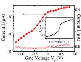
Finite source-drain bias regime.—Driving mesoscopic and nanoscopic devices out of equilibrium by applying a finite bias voltage typically corrupts their quantum coherence (e.g., electrons at different energies within a bias voltage window have different interference patterns), so that standard interference effects are observed in the linear response regime Nazarov2009 . Concurrently, at finite bias voltage between the source and drain electrodes, the attached third electrode as in the device in Fig. 1(a) would draw finite current Cardamone2006 , which is an example of leakage currents whose minimization is one of the major tasks in downscaling FETs in digital electronics Schwierz2010 . Here we use the setup in Fig. 1(b) to investigate the range of modulation of source-drain current at V via the top gate positioned at the distance 5.3 Å away from the device. Figure 4 shows that current can be modulated from very small to finite value by changing the gate voltage , while the selected distance ensures that tunneling leakage current into the top electrode is very small. Thus, this type of a device could act as either a molecular-scale FET Song2009 or as a bipolar junction transistor capable of amplifying current in the third lead.
Conclusions.—In conclusion, using NEGF-DFT formalism, recently extended to multiterminal devices Saha2009a , we analyzed quantum transport through ZGNR18-annuleneZGNR junction in the presence of the third ZGNR electrode attached either as the infinite-impendence voltage probe or serving as the “air-bridge” top gate covering half of the molecular ring. While both choices for the third electrode disrupt destructive quantum interferences (responsible for exponentially small transmission in the corresponding two-terminal device), transmission increases substantially further when using the “air-bridge” top gate which enhances the LDOS underneath to directly connect the source and the drain. Moreover, the latter device in its ‘on’ state even approaches the long-sought limit Kiguchi2008 in molecular electronics of a unit transmission through an organic-based device with a single conducting channel, because of high contact transparency brought by the proposed application of graphene-based electrodes.
Acknowledgements.
We thank M. Grifoni and K. Richter for illuminating discussions. Financial support through NSF Grant No. ECCS 0725566 (K. K. S. and B. K. N.), DFG SFB 689 (during stay of B. K. N. at the University of Regensburg) and DOE Grant No. DE-FG02-98ER45685 (W. L. and J. B.) is gratefully acknowledged. The supercomputing time for this research was provided in part by the NSF through TeraGrid resource TACC Ranger under Grant No. TG-DMR100002 (K. K. S. and B. K. N.).References
- (1) X. R. Wang et al., Phys. Rev. Lett. 100, 206803 (2008).
- (2) J. Cai et al., Nature 466, 470 (2010).
- (3) F. Schwierz, Nature Nanotech. 5, 487 (2010).
- (4) D. Areshkin and C. White, Nano Lett. 7, 3253 (2007).
- (5) M. Kiguchi et al., Phys. Rev. Lett. 101, 046801 (2008); L. Venkataraman, Physics 1, 5 (2008).
- (6) Introducing Molecular Electronics, edited by G. Cuniberti, G. Fagas, and K. Richter (Springer, Berlin, 2005).
- (7) S.-H. Ke, H. U. Baranger, and W. Yang, Phys. Rev. Lett. 99, 146802 (2007).
- (8) F. Cervantes-Sodi et al., Phys. Rev. B 77, 165427 (2008).
- (9) H. Song et al., Nature 462, 1039 (2009).
- (10) K. Stokbro et al., Comp. Mat. Science 27, 151 (2003).
- (11) X. Guo et al., Science 311, 356 (2006).
- (12) O. V. Yazyev and M. I. Katsnelson, Phys. Rev. Lett. 100, 047209 (2008).
- (13) D. A. Areshkin and B. K. Nikolić, Phys. Rev. B 79, 205430 (2009).
- (14) J. Jiang, W. Lu, and J. Bernholc, Phys. Rev. Lett. 101, 246803 (2008).
- (15) D. M. Cardamone, C. A. Stafford, and S. Mazumdar, Nano Lett. 6, 2422 (2006); C. A. Stafford, D. M. Cardamone, and S. Mazumdar, Nanotech. 18, 424014 (2007).
- (16) Y. V. Nazarov and Y. M. Blanter, Quantum Transport: Introduction to Nanoscience (Cambridge University Press, Cambridge, 2009).
- (17) J. Rincón et al., Phys. Rev. Lett. 103, 266807 (2009); T. Hansen et al., J. Chem. Phys. 131, 194704 (2009); T. Markussen, R. Stadler, and K. S. Thygesen, Nano Lett. 10, 4260 (2010).
- (18) D. A. Areshkin and B. K. Nikolić, Phys. Rev. B 81, 155450 (2010).
- (19) S.-H. Ke, W. Yang, and H. U. Baranger, Nano Lett. 8, 3257 (2008).
- (20) K. K. Saha et al., J. Chem. Phys. 131, 164105 (2009).
- (21) D. Darau et al., Phys. Rev. B 79, 235404 (2009).