Possibilities of application of elastic mid-IR light scattering for inspection of internal gettering operations
Abstract
A method of low-angle mid-IR light scattering is shown to be applicable for the contactless and non-destructive inspection of the internal gettering process in CZ Si crystals. A classification of scattering inhomogeneities in initial crystals and crystals subjected to the getting process is presented.
1 Introduction
Recently, the internal gettering process became one of the main operations for manufacturing of semiconductor devices of CZ Si. However, methods for the direct inspection of the internal gettering efficiency and stability have been practically absent thus far. The purpose of this paper is to present such a method developed on the basis of law-angle IR-light scattering technique (LALS) [1], which has been successfully applied thus far for the investigation of large-scale electrically active defect accumulations (LSDAs) in semiconductor crystals (see e.g. [2] and references therein).
A method of LALS was applied at the first time to the investigation of the influence of both the internal and external gettering processes on large-scale impurity accumulations (LSIAs 111LSIAs are a type of LSDAs which contain mainly impurities rather than intrinsic defects.) in crystals of the industrial CZ Si:B in Ref. [3]. The conclusions were made in Ref. [3] that (i) the external gettering process resulted in a considerable decrease of the impurity concentration in LSIAs and (ii) new defects arose in the crystal bulk as a result of the internal gettering process which became a predominating type of defects.
The current work presents an application of LALS with the non-equilibrium carrier photoexcitation [1, 4] to the studies of the internal gettering process in addition to the conventional LALS measurements.
The LALS temperature dependences are also presented and the activation energies of the centers constituting the LSIAs are estimated in this work.
2 Experimental
A continuous 10.6-m emission of a CO2-laser was used as the source of the probe radiation in LALS. All the details of this technique are described in Refs. [1, 2]. We would like to remind only that such parameters of LSDAs as their effective sizes and the product of the LSDA concentration by the square of the deviation of the free carrier concentration (or the square of the dielectric constant variation) in LSDAs (or ) can be calculated from the light-scattering diagrams.
The investigation of the influence of a sample temperature on its light scattering enables the estimation of the thermal activation energies () of impurities and defects composing the LSDAs — [5]. During the low-temperature measurements, the sample temperature varied from 80 to 300K.
The influence of non-equilibrium carrier photoexcitation on light scattering was studied as well. The essence of the experiments consist in the following. If a crystal contains large-scale centers of recombination (e.g. precipitates and their colonies, stacking faults, swirls, etc.), regions with decreased concentration of non-equilibrium carriers are formed around these centers during the process of the non-equilibrium carrier generation. These regions scatter the light like usual nonuniformities and when pulse generation of carrier is used, the scattered light pulses are observed in LALS. Selecting this pulsed component, it is possible to register the light scattering by recombination defects (RDs). Then the usual procedure of the light-scattering diagram measurement and treatment is applied to estimate the dimensions of the depleted regions around RDs [1, 4]. In this work, the non-equilibrium carrier was generated by 40-ns pulses of YAG:Nd3+-laser at the wavelength of 1.06 m, frequency of 1 kHz and mean power of 1 W. The photoexcitation at this wavelength pumps whole the crystal bulk practically uniformly, as the absorption for this wavelength is not too high but sufficient to produce the efficient enough electron-hole pair generation. The scheme of the used instrument is described in detail in Refs. [1, 4].
Electron beam induced current (EBIC) and selective etching (SE) were used to reveal the defects as well. During the sample preparation for EBIC, a special technique was used which included the plasma etching of the sample surface in special regime before the Schottky barrier was created. This technique considerably increases EBIC sensitivity to RDs in bulk Si [6].
About 40 wafers of dislocation-free Si were studied. The crystals were produced by Czochralski method and doped with boron (CZ Si:B) up to the specific resistivity from 1 to 40 cm. The crystals were produced at three different establishments and subjected to the internal gettering process at five different establishments. In this paper, the effect of different gettering regimes on defects is summarized. In the experiments on LALS, the two following schemes of experiment were used. In one scheme, a preliminary study of the as-grown substrates, which then were subjected to the internal gettering process and examined by LALS, was carried out. In the other scheme the substrates were cut into several parts. Some of these parts were subjected to the gettering process and the other parts were used as the reference samples.
Experiments on EBIC and SE were carried out only in accordance with the second scheme.
3 Results
3.1 As-grown samples
The studied here initial wafers contained a standard for CZ Si:B set of LSIAs [7]. In these samples, so-called cylindrical defects (CDs) with the lengths from 15 to 40 m and diameters from 5 to 10 m were observed in the EBIC microphotographs (Fig. 1 ). The concentration of CDs was estimated as 106–107 cm-3.
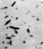
In the scattering diagram (Fig. 3, curve 1) these defects correspond to the sections at . So-called spherical defects (SDs), the concentration of which in initial samples did not exceed 105 cm-3, were also observed (Fig. 1 ). The dimensions of these defects were from 5 to 15 m. These defects correspond to the sections at in the scattering diagram (Fig. 3, curve 1).
3.2 After internal gettering
The main result for the crystals subjected to the internal gettering process are as follows:
1. As a result of the internal gettering, SDs with the dimensions from 10 to 30 m (Fig. 1; Fig. 3, curve 2), became the predominating type of defects, and for these defects became by two orders of magnitude greater in comparison with that for the initial material. for CDs changed rather weakly and this led to prevalence of scattering by SDs in the scattering diagrams of the substrates subjected to the internal gettering. We can conclude that the concentration of SDs considerably increased as a consequence of the internal gettering (Fig. 1 ). The increase of and the SD concentration after the internal gettering was the common


phenomenon for all the studied samples. This phenomenon did not depend on the gettering regime. The increase of SD-related correlated with the appearance of the gettering defects revealed by SE. We did not obtain a proportional dependance of SD-related on epd, however .
2. It was found that significantly increased after the internal gettering and a good correlation of with epd was observed (Fig. 3, curve 2).
3. The values of the activation energies () of the centers predominating in SDs, perhaps, are defined by the growth conditions and the thermal prehistory of a sample. For example in Fig. 4, SD-related temperature dependences are shown for two samples grown at different establishments and subjected to the internal gettering. It is seen that these dependences and the values of are absolutely different for these samples — 130–170 meV for sample 1 and 60–90 meV for sample 2. So, different point centers constituted SDs in these samples after the internal gettering. Nowadays we have not got enough data to be sure what of the following factors defines the SD composition: the initial material parameters or the gettering process peculiarities. We think that the first factor is more important.
4 Discussion
On the basis of the above we assume that RDs in the substrates subjected to the internal gettering are defects of structure (most likely, they are precipitates and their colonies) which are formed in the wafer bulk during the gettering process, and are the gettering defects. As for SDs, they are the impurity atmospheres around these defects. These atmospheres are formed when impurities flow to the gettering defects 222It is important to note that impurity atmospheres consist at least of two components: the dissolved impurities and the impurity precipitates. In the conventional LALS experiments — without photoexcitation — only the first component is observed.. These conclusions are confirmed by the correlation of RD-related with epd and the increase of SD-related after the appearance of a great number of defects revealed by SE.
For any inhomogeneity, where is the defect concentration and is the deviation of the dielectric constant inside them. In the case of RDs, is determined first of all by the generated excess carrier concentration. At equal levels of photoexcitation RD-related for the crystals with different . So in this case is a straightforward measure of the RD concentration in crystals. In the case of impurity atmospheres, the situation is much more complicated. in them is controlled by many parameters: the average concentration of impurities in SDs,

the ratio of the dissolved and precipitated impurity concentrations, the compensation degree, etc. The gettering process may change both and any of these parameters which will result in the violation of the proportionality to in experiments. Hence in the case of SDs, we are forced to rely only upon a qualitative correlation which is observed in the experiment 333Now new techniques of scanning LALS (SLALS and OLALS) have been developed which enable the direct visualization of defects and accurate estimation of their parameters [8]. These techniques are very promising for the internal gettering investigation [9]..
On the basis of the above, we suggest the following method for the examination of the gettering process in silicon substrates.
The RD-related light scattering measurements (LALS with photoexcitation) enable the inspection for the presence and stability of the gettering defects in the substrate bulk.
The investigation of SD-related light scattering (conventional LALS measurements) enables the inspection the presence and dimensions of the impurity atmospheres around the gettering defects, i.e. the efficiency of the gettering operations.
Note that the main advantage of this technique is its applicability for the input and technological step inspection of substrates during the whole technological cycle. It enables the examination of stability and efficiency of the gettering process after any high-temperature operations. The equipment may be easily adapted for the technological process; it allows one to carry out the express (for 1 or 2 minutes) testing and mapping of substrates of any diameter.
The studies of temperature dependences enable the analysis of the impurity atmospheres composition, i.e. they allows one to determine what impurities are gathered by the gettering defects from a free zone. In this case it is reasonable to speak of a random inspection or laboratory research.
5 Conclusion
In conclusion, we would like to pay your attention upon a very promising potentiality.
It is possible to carry out the nondestructive input and technological step
inspection for the presence of RDs not only in a wafer bulk but
directly in the boundary zone. The proposed technique is
analogous to the method of RD revealing in a substrate bulk, but
instead of the “bulk” excitation of the electron-hole pairs it is proposed
to use
the “surface” photoexcitation (e.g. using short pulses of
the second harmonic of
YAG:Nd3+-laser, m). In this case,
the non-equilibrium carriers will penetrate
into the depth
of 10–20-m subsurface layer, and just this layer will be analyzed
for the
content of recombination-active defects of structure and
precipitates. The main difficulty here is the small but
the preliminary experiments demonstrated the possibility of
registration of light scattering from layers with the RD
concentration down to 104–105 cm-3.
This technique is undoubtedly very
promising since it will allow one to directly determine a degree of
purification of the free zone rather than processes developing
in the wafer bulk. For instance, it would enable the inspection of the
effect of precipitates “germinating” in the free zone during
the technological cycle. Note also that this technique is
suitable not only for solving the problem of gettering but
also for the examination of any epitaxial and boundary layers.
References
- [1] Kalinushkin V P 1988 Proc. Inst. Gen. Phys Acad Sci USSR vol 4 Laser Methods of Defect Investigations in Semiconductors and Dielectrics (New York: Nova) pp 1–79
-
[2]
Kalinushkin V P, Yuryev V A and Astafiev O V 1994 1st Int. Conf.
on Materials for Microelectronics, Barcelona, 17–19 October 1994
Kalinushkin V P, Buzynin A N, Astafiev O V et al1996 Inst. Phys. Conf. Ser. 149 219–24 Kalinushkin V P, Yuryev V A and Astafiev O V 1999 Rev. Sci. Instrum. 70 4331–43 - [3] Gulidov E N, Kalinushkin V P, Murin D I et al1985 Sov. Phys.– Microelectronics 14 (2) 130–3
- [4] Kalinushkin V P, Murin D I, Murina T M et al1986 Sov. Phys.– Microelectronics 15 (6) 523–7
-
[5]
Kalinushkin V P, Yuryev V A, Murin D I and Ploppa M G 1992 Semicond.
Sci. Technol. 7 A255–62
Kalinushkin V P, Yuryev V A 1995 Mater. Sci. Eng. B 33 103–14
Kalinushkin V P, Yuryev V A and Murin D I 1991 Sov. Phys.– Semicond. 25 (5) 798–806
Voronkov V V, Voronkova G I, Kalinushkin V P et al1984 Sov. Phys.– Semicond. 18 (5) 938–40
Zabolotskiy S E, Kalinushkin V P, Murin D I et al1987 Sov. Phys.– Semicond. 21 (8) 1364–8 - [6] Buzynin A N, Butylkina N A, Lukyanov A E et al1988 Bul. Acad. Sci. USSR. Phys. Ser. 52 (7) 1387–90
-
[7]
Buzynin A N, Zabolotskiy S E, Kalinushkin V P et al1990
Sov. Phys.– Semicond. 24 (2) 264–70
Astafiev O V, Buzunin A N, Buvaltsev A I et al1994 Sov. Phys.– Semicond. 28 (3) 407–15 -
[8]
Astafiev O V, Kalinushkin V P and Yuryev V A 1994 Proc. SPIE 2332 138–45
Astafiev O V, Kalinushkin V P and Yuryev V A 1995 Mater. Sci. Eng. B 34 124–31
Astafiev O V, Kalinushkin V P and Yuryev V A 1996 Inst. Phys. Conf. Ser. 149 361–6 -
[9]
Astafiev O V, Kalinushkin V P and Yuryev V A et al1994 Proc. SPIE 2332 146–53
Astafiev O V, Kalinushkin V P and Yuryev V A et al1995 Proc. 1995 MRS Spring Meeting vol 378 ed S Ashok, J Chevallier et al(Pittsburgh: Material Research Society) 615–20
Astafiev O V, Kalinushkin V P and Yuryev V A 1995 Inst. Phys. Conf. Ser. 146 775–80