Band engineering in graphene with superlattices of substitutional defects
Abstract
We investigate graphene superlattices of nitrogen and boron substitutional defects and by using symmetry arguments and electronic structure calculations we show how such superlattices can be used to modify graphene band structure. Specifically, depending on the superlattice symmetry, the structures considered here can either preserve the Dirac cones ( superlattices) or open a band gap (). Relevant band parameters (carriers effective masses, group velocities and gaps, when present) are found to depend on the superlattice constant as where is in the range , depending on the case considered. Overall, the results presented here show how one can tune the graphene band structure to a great extent by modifying few superlattice parameters.
I Introduction
Single layer graphene is a very promising material for a future
silicon-free nanoelectronics. The peculiar character of its charge
carriers comes from the intersection of the electronic bands occurring at the corners
of its hexagonal Brillouin zone. This gives rise to the so-called Dirac cones at the Fermi level
and makes graphene a zero-gap semiconductor Slonczewski and Weiss (1958) in which
low energy excitations behave as massless,
chiral Dirac particlesCastro Neto et al. (2009); Abergel et al. (2010).
In turn, this implies a series of interesting physical effects that open new
perspectives for fabricating novel electronic devicesSchwierz (2010),
e.g. high-performance transistors for radiofrequency
applicationsLin et al. (2009); Avouris (2010).
In this perspective the possibility of engineering
graphene’s band structure by introducing defects, strains or
external potentials
has gained importance in the recent past, in particular for opening a
gap in the band structure
which is essential to design logic devices.
Indeed the non-vanishing residual conductance of intrinsic graphene
avoids the complete current pinch-off in the pristine
materialPeres (2010); Avouris et al. (2007),
thereby limiting the on-off ratio to .
A number of controlled techniques for energy band engineering have been
proposed other than the actively pursued goal to obtain nanoribbons
of controlled size and edge geometry.
Most of them are based on the use of superlattices of external potentials
Tiwari and Stroud (2009); Park et al. (2008) or defects such as
holesPedersen et al. (2008); Liu et al. (2009)
and adsorbates Chernozatonskii and Sorokin (2010).
Controlled vacancies on graphene Fischbein and Drnić (2008),
as well as large holes symmetrically arranged to form
graphene anti-dots Bai et al. (2010)
have actually been realized with modern lithographic and
self-assembling techniques.
Preferential sticking of atoms induced by Moiré patterns
Balog et al. (2010) or by other electronic effects
Cheianov et al. (2009, 2010) could also induce a superlattice ordering that
modifies graphene energy bands. Likewise, there is a great hope that
novel bottom-up techniques Bieri et al. (2009)
may be applied
to fabricate atomically precise graphenic structures
as already shown for nanoribbonsCai et al. (2010).
These approaches might allow to realize in the near future graphene-related
two-dimensional materials with modified characteristics,
e.g. linearly-dispersing bands with variable Fermi velocities or
semiconducting structures.
In this paper we focus on atomically precise superlattices
of substitutional atoms.
The present work connects to and extend a recent workMartinazzo et al. (2010)
where we have shown that
in properly designed superlattices of holes or adatoms one can open a gap
without breaking graphene point symmetry, i.e. preserving
the pseudo-relativistic behaviour of charge carriers which makes graphene so
attractive. The structures suggested in Ref.(Martinazzo et al., 2010) have
vacancies (hence missing orbitals) at the sites of a honeycomb
superlattice, as a consequence of the
introduction of C vacancies (holes) or chemisorption of simple atomic species.
Here we consider similar, highly symmetric structures, but with
vacancies replaced by boron and nitrogen.
Similar defects have been recently considered for tuning the electronic
properties
of graphene nanoribbons and other carbon based structures suggesting that,
when arranged to form particular structures, they can turn the material into
a semiconductor or a half-metalDutta et al. (2009); Dutta and Pati (2008); Zheng et al. (2010).
Half-metallicity and the other many-body effects in such a
structures open new perspectives in the field of carbon-based materials
for spintronic
applications: for a recent review see Ref.Yu and Zheng (2010); Dutta and Pati (2010)
and references therein.
In this paper we show that, depending on the superlattice symmetry, one can
obtain either electron (hole) doped substrates with pseudo-relativistic
massless
carriers or semiconducting structures with a quasi-conical dispersion, and
with the help of electronic structure calculations (tight-binding and density-functional theory)
we determine carriers velocities, effective masses and band gaps (when present) as functions of the superlattice .
The focus is on boron and nitrogen, mainly because of the fast progresses
in methods for the controlled synthesis of B and N doped graphenes.
For instance, Panchakarla et al.Panchakarla et al. (2009) have
recently shown how it is possible to insert B or N dopants in graphene by
adding the correct precursors in the arc discharge chamber, while Ci et al.Ci et al. (2010)
have reported the synthesis of large islands of boron
nitride embedded in graphene by atomic layer deposition techniques. Methods
to selectively replace C atoms in the graphene lattice have also been
proposed Pontes et al. (2009), thereby suggesting that the superlattice structures
considered in this paper might soon become feasible.
The paper is organized as follows. In the next section we summarize the
computational details of the calculations.
Then, we show how -(-) doped graphene-like structures result
when substitutional defects are arranged in honeycomb superlattices,
whereas semiconducting structures with quasi-conical dispersion (massive
Dirac carriers) result either from a hexagonal superlattice of from
a honeycomb co-doped superlattice. Finally, we summarize and conclude.
Throughout this paper we define the superlattice periodicity using Wood’s notation, i.e.
by multiplying graphene’s two-dimensional lattice vectors by the integer
(superlattice) constant .
II Computational Methods
The results shown in the next sections have been obtained
from both tight-binding (TB)
and density functional theory (DFT) electronic structure calculations.
In the first case we diagonalized the usual tight-binding Hamiltonian
for graphene system, applying periodic boundary conditions
and including hopping terms up to the third nearest-neighbors.
The on-site energies and hopping terms , and
(for nearest, next-to-nearest and next-to-next-nearest neighbors,
respectively)
are those proposed by Nanda et al.Nanda and Satpathy (2009).
They were fitted to accurate all-electron calculations to correctly reproduce
the Fermi velocity of single layer graphene.
For the dopant atoms we only considered hoppings to nearest neighbor sites.
Their values (), as well as those of the on-site energies (),
are those introduced by Peres et al.Peres et al. (2007), who have
already successfully used them to study electronic effects in doped graphene.
A summary of the TB parameters is listed in 1.
| Atom | ||||
|---|---|---|---|---|
| C | 0.000 | -2.900 | +0.175 | -0.155 |
| B | -1.5225 | +1.450 | - | - |
| N | +1.5225 | -1.450 | - | - |
First principles DFT calculations were
preformed with the help of the VASP suite Kresse and Hafner (1994, 1993), using a
supercell approach. Core electrons were taken into account
by projector augmented wave (PAW) pseudo-potentials while for valence a
500 eV plane wave cutoff was used. To correctly represent the defect
induced charge inhomogeneities we used the Perdew-Burke-Ernzerhof
(PBE) gradient-dependent exchange and correlation functional Perdew et al. (1996).
Band structures were sampled by a centered -points grid,
never sparser than 6x6x1 in order to include every special point in the Brillouin zone (BZ).
The TB parametrization was tested by comparing the band structure of few
superlattices along the -K-M-K’- path with accurate
DFT results.
In every case the adopted parametrization was found to be accurate enough
to reproduce the bands close to the Fermi energy.
Therefore, we computed DFT band structures
for x graphene superlattices up to =14, and for larger structures
we relied on TB calculations only.
III Results and Discussion
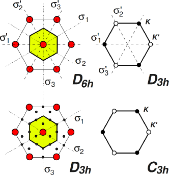
Graphene’s peculiar electronic structure is strictly related to the point symmetry of its lattice, in the Shönflies notation. In the Brillouin zone, for each Bloch electronic state with vector , the relevant symmetry elements are those which either leaves invariant or transforms it into one of its equivalent images, i.e. being a reciprocal lattice vector. These elements form a subgroup of , known as little co-group or simply -group at Mirman (1999), which determines the possible symmetries of the electronic states at . At the high symmetry point (or ) of graphene’s Brillouin zone the -group is , and Bloch functions built as linear combinations of orbitals span a two-dimensional irreducible representation (irrep) of such a symmetry group (). This is enough for the degeneracy and the unusual linear dispersion at (). That this occurs exactly at the Fermi level is a consequence of the electron-hole () symmetry which approximately holds in graphene. Indeed, thanks to this extra symmetry, energy levels are always symmetrically arranged and, at half-filling, the Fermi level lies exactly at the center of the spectrum, where any doubly degenerate level is forced to lay 111 Notice that even though symmetry only holds in the nearest neighbors approximation and in absence of diagonal disorder, the Fermi level always matches the doubly degenerate state at () as long as the symmetry breaking does not cause the maximum (minimum) of the valence (conduction) band to exceed the energy at . . In general, the number of doubly degenerate irreps in the BZ determines alone the presence of states (absence of a gap) at the Fermi level. We have recently shownMartinazzo et al. (2010) how one can turn such number to be even at every special point -thus opening a gap in the band structure- by symmetrically removing “ orbitals” in forming certain x superlattices. Substitutional defects behave similarly to vacancies (to which they reduce when the hoppings become zero) but introduce impurity bands which partially hybridize with those of the substrate. In addition, the diagonal disorder they introduce breaks symmetry giving rise to a Fermi level shift, to and doping for group IIIA and VA elements, respectively, as recently shown for both graphene Lherbier et al. (2008) and nanotubes Zheng et al. (2010) . In the weakly defective superstructures considered in the following the defect-induced perturbation affects the electronic structure close to the Fermi level. With homogeneous doping the latter shifts at most proportionally to , i.e. as the square root of the defect concentration, as a consequence of the linear-energy dispersion which implies , where is the Fermi velocity of pristine graphene and is the electron (hole) excess density, . Hence, analogously to the superlattices of vacanciesMartinazzo et al. (2010), we make use of symmetry arguments to establish whether degeneracy occurs at the BZ special points in the important low-energy region.
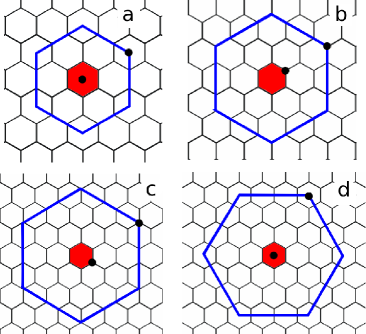
It is worth noticing at this point that, however small the defect perturbation is, the folding of graphene band structure occurs differently according whether the superlattice constant belongs to the sequence or ( integer). As shown in 1 for the superlattices considered in this work (a-c), for () and fold separately into () and (), whereas for they both fold to the BZ center . This means that superlattices are expected to have rather unique properties related to the highly degenerate nature of the unperturbed spectrum. In the following we mainly focus on superlattices and only occasionally look at the properties of ones. A further six-fold superlattice symmetry, the x case reported in 1(d), will not be considered here since in that case band folding occurs analogously to the x case discussed above.
III.1 Honeycomb superlattices
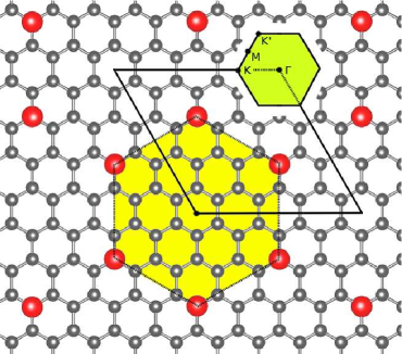
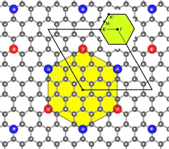
A honeycomb-shaped superlattice is a natural choice for x
superlattices (x-honeycombs thereafter),
since it preserves the point group symmetry of pristine graphene.
The superlattice unit cell contains two substitutional atoms and is shown in 2.
If the atomic radii of the dopants are small enough that lattice distortions are minimal,
the system overall symmetry is preserved and Dirac cones at and are expected.
This is the case of boron and nitrogen substitutional defects, whose DFT-optimized structures
show no appreciable lattice distortion. Both TB and DFT calculations confirm that and
honeycomb superlattices made of B or N substitutional defects only show a low-energy band structure very
similar to that of perfect graphene, but with the Fermi level lying respectively below (-doped)
and above (-doped) their Dirac point. In principle, with properly designed or back-doping,
e.g. electric-field induced but also via molecular adsorptionColetti et al. (2010); Pinto et al. (2010),
such shift can be offset and the analogy with pristine graphene can be fully exploited.
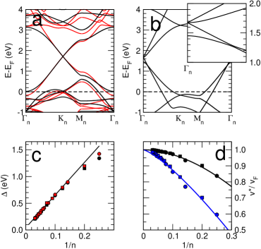
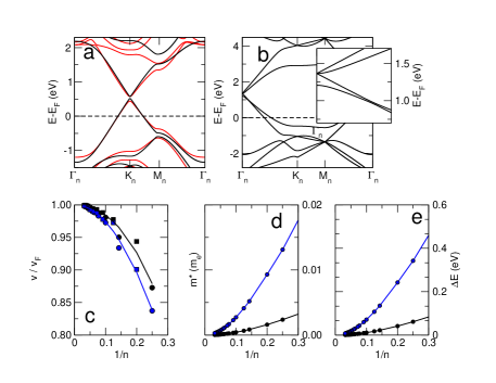
3(a) shows the TB and first principles band structures of one x-honeycomb together with the position of the Fermi level (3(c)) in such - and -doped superlattices at different impurity concentrations. As expected, the shift () of the Dirac cones with respect to the Fermi level (see 3(c)) is, to a good approximation, inversely proportional to the dopant concentration for both B and N doping, though with opposite sign. The difference between TB and DFT band structure is minimal, and this confirms that the tight binding parameters adopted are good enough for accurately describing the low-energy features of the x-honeycomb superlattices investigated in this paper. In 3(b) we also report the unique band structure resulting from the special folding in the sequence; as it is evident from the inset of 3(b), the four-fold degeneracy occurring at is partially lifted, and a gap is introduced in one of the two cone replica.
The group velocity for electrons and holes taken close to the cone apex (but rather adequate for a wider energy range) is shown in 3(d) for - and -doped superlattices. The two curves approach the limit of clean graphene with different trends. Upon non-linear curve fitting the group velocity (relative to the one in pristine graphene) for -doped honeycombs is found to behave as , while for -doped honeycombs as . The difference between the two cases is due to the value of the on-site energies and hopping of the dopants which determine the degree of hybridization of their impurity levels with that of bulk graphene. With the parameters used (see 1), which are symmetric with respect to the on-site energy of C atoms, this can only happen because of the asymmetry in graphene electronic structure introduced by the next-to-nearest neighbor interactions. Other superlattices made of group IIIA (Al, Ga, In) and VA (P, As, Sb) dopants have been tested by first principles calculations. In any case we found that, after geometric optimization of the lattice structure, the impurities stand out from the graphene layer plane and considerably distort the neighboring lattice positions. The resulting band structures are metallic but lack of Dirac cones due to the reduced symmetry.
III.2 Hexagonal superlattices
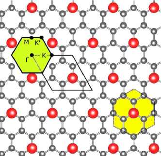
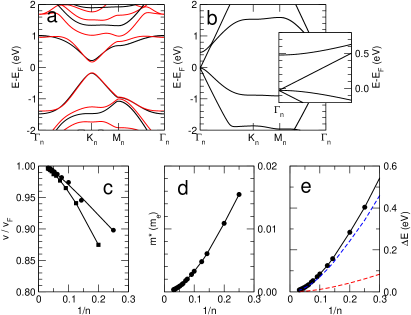
When one defect per supercell only is introduced a x hexagonal superlattice (a “x-hexagon”) results, as shown in 4. This kind of structures is closely related to the honeycomb ones, having one extra substitutional atom at the center of a hexagon of defects. A closer inspection, however, reveals that, due to the presence of the underlying C network, the point symmetry is reduced to , with planes missing with respect to the honeycomb counterparts. It follows that the -group at () is , with no irreducible two-dimensional (complex) representations (see 5). Hence, degeneracy is removed at the special points and a (small) gap opens in the band structures, close to the (shifted) Fermi energy. This is shown in 6(a) where the TB and DFT band-structures of the x hexagon are reported. The energy spectrum of such gapped graphene is compatible with charge carriers behaving as massive Dirac particles
| (1) |
where are the effective ‘speed of light’ and ‘rest mass’, respectively, and determine the gap size
| (2) |
According to the semiclassical theory of conduction is also the effective mass governing charge carrier mobility for ; for carriers behave pseudorelativistically with and limiting speed . The values , and have been obtained by non-linear curve fitting of the numerical results to 1 and are reported in panels (b)-(d) of 6.
For x-hexagons the band gap is very dependent on the type of dopant (6.(e)): the maximum gaps, occurring in x hexagons, are 0.93 eV for nitrogen and only 0.17 eV for boron. The effective masses of electrons and holes (6.(d)) roughly scale as the gaps: and for - and -doped structures respectively, and their maximum is 3.7x and 6.7x . This is similar to the case of graphene nanoribbonBarone et al. (2006), whose band gap scales as the inverse of their width even though here the gap is due to symmetry breaking rather than quantum confinement. The shift of the Fermi level (not shown) is again proportional to the square root of the defects concentration, that is now only half of the value for honeycombs with the same superlattice periodicity. Charge carriers velocities scale similarly for the two dopant species as shown in 6.(c) with a best-fit exponent close to -2 (, ). In 6, panel (b), we also report the particular band structure arising in hexagon superlattices. At the relevant special point , the massive, pseudo-relativistic energy dispersion is superimposed with a massless one, thereby giving rise to a two-valley system with very different charge carriers. As shown in the next subsection, all the features discussed in this Section can be brought at the Fermi level by co-doping the substrate in forming a honeycomb structure with the same symmetry discussed here.
III.3 Co-doped superlattices
One further possible superlattice arrangement is obtained by using two different dopants in the x-honeycomb unit cell, i.e. co-doping the structures with boron and nitrogen (see 7). In this way B and N atoms form a boron nitride-like honeycomb superlattice in which sublattices equivalence (and symmetry) is broken.
This is analogous to place graphene in the modulating field of a proper substrate, e.g a hexagonal BN (0001) surface, which has been shown to lift the degeneracy of the bands Giovannetti et al. (2007); similarly for deposition, or growth, on silicon carbide surfaces Mattausch and Pankratov (2007); Varchon et al. (2007). The superlattice structures considered here offer the possibility to modify the periodicity of the perturbation, and thus to tune the gap. Indeed, this kind of superlattices present point symmetry, hence a -group in , and, analogously to the hexagonal case discussed above, open a band gap typical of massive Dirac particles. Differently from before, however, the structures considered here are iso-electronic with graphene and therefore the gap lies exactly at the Fermi energy.
8 shows the computed band structure (panel (a)), together with the values of the effective speed of light (c), effective mass (d) and band gaps (e), obtained as in previous section by fitting of the numerical results, for different BN x-honeycombs. The results confirm the expectations, and show that such structures present a band-gap at the Fermi energy, compatible with pseudo-relativistic massive carriers. Their effective rest mass is rather small, scales as and it is never larger than 0.016 for . This value compares favorably with the effective masses in Bi1-xSbx topological insulators (=0.009 ) Hsieh et al. (2008), and is generally lower than in bilayer graphene (=0.03 )Castro et al. (2008) or in any other traditional bulk semiconductors, such as InSb (=0.016 ). Since is the main factor affecting carrier mobility, the suggested structures turn out to be a good compromise between the need of opening a gap for logic applications and the desire of preserving the high mobility of charge carriers. In 8, panel (b) we also report the band structure of the case. The structure is that of a zero-gap semiconductor, with two distinct charge carriers: one of them behave as electron (hole) in graphene, showing typical effects expected for massless carriers; the other is a more conventional one, with a finite excitation energy across a gap.
IV Summary and Conclusions
To summarize, we have studied the effects substitutional defects such B and N species
have on graphene electronic structure when they are periodically arranged to form some superlattices.
Using group theoretical arguments and both TB and DFT calculations we have shown
that defects can either preserve the Dirac cones or open a band gap,
depending on the superlattice symmetry ( and , respectively).
Specifically, honeycomb-shaped superlattices of B or N atoms give rise to - and -doped graphene,
respectively, preserving the Dirac cones.
On the other hand, when a hexagonal superlattice is formed,
or the honeycomb one is symmetrically co-doped, the Dirac cones detach from each other to form
a gapped, quasi-conical structure whose excitations correspond to massive Dirac particles.
Note that this situation clearly differs form the case of randomly arranged
B or N impurities, in which the density of states shows no band gap Lherbier et al. (2008).
For zero-gap structures the use of this superlattices offers the possibility
to control the Fermi velocity by changing the structure periodicity,
thereby offering the opportunity to investigate
its role in the charge transport properties.
Differently from our recent proposalMartinazzo et al. (2010),
the gapped band structures arise because of symmetry breaking,
as in the case of graphene interacting with a substrate such as
SiC or BN. In the same fashion the band gap size depends
on the superlattice periodicity.
In our calculations we have found that gaps and charge carriers velocities
effective masses
depends on , where is in the range , hence on some small power
of the dopant concentration, and on the dopant type (B or N).
Overall the structures proposed here show a band gap larger than at
room temperature, with an effective mass generally lower that 0.01
for reasonably dense meshes (=4-10).
Thus, the new class of graphene structures proposed might be promising candidates for the fabrication of
high performance interconnects, valley-based devicesXiao et al. (2007),
but also for logic transistors, where a band gap is needed, but the extraordinary properties
of pristine graphene need to be preserved.
The electronic properties of these impurities superlattices rely on symmetry,
hence are necessarily sensitive to the dopant positions.
As a consequence, an accurate control of the system geometry is
necessary to exploit their properties. This might be possible in the near future
with precise bottom-up techniques, such as the ones recently used by Ruffieux and co-workers
Cai et al. (2010); Bieri et al. (2009) to fabricate nanoribbons of well-defined widths and edges.
An indication of the possible synthetic routes together with
formation energies for such defects superlattices can be found in the Supporting Information.
This information is available free of charge via the Internet at http://pubs.acs.org.
V Supporting information
In order to compare relative structural stabilities, formation energies for superlattice structures have been computed as follows:
| (3) |
where is the total energy of the structure, is the superlattice constant,
is the number of dopants per cell (1 for hexagons and 2 for honeycombs),
and are the number of atoms and the chemical potentials
for each species. The chemical potentials were computed with respect to single layer graphene,
gaseous N2 and -Boron (in the so-called R12 structure). Density functional theory results
are shown in 2 and in figure 9.
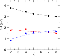
| Hexagon | Honeycomb | ||||
|---|---|---|---|---|---|
| B | N | B | N | BN | |
| 2 | 1.840 | 1.078 | 3.780 | 1.754 | 0.841 |
| 4 | 1.513 | 0.878 | 3.455 | 1.871 | 1.500 |
| 5 | 1.499 | 0.933 | 3.224 | 1.622 | 1.593 |
| 7 | 1.380 | 0.676 | 3.063 | 1.596 | 1.626 |
| 8 | 1.394 | 0.695 | 3.005 | 1.490 | 2.023 |
For all the cases considered the formation energy of the superlattice structures is endothermic
with respect to the pure elements with opposite trends for - (-)doped and co-doped structures.
While two impurities of the same kind gain energy when lying further apart to each other, B and
N tend instead to cluster together, in accordance with recent experimental observations Ci et al. (2010).
However, in order to cluster the impurities have to diffuse through the graphene lattice by exchanging
its position with a carbon atom. Such a process has a large energetic barrier being the two atoms
covalently bound, hence the kinetics of this process is expected to be extremely slow.
We therefore suggest that these structures are expected to be stable at room temperature as well as other known structures
(e.g. graphene itself with respect to diamond).
About the practical feasibility of substitutional defects superlattices we expect they can be produced by the same
bottom-up approach recently used to fabricate graphene structures
with atomic-scale controlBieri et al. (2009); Cai et al. (2010).
According to this method an appropriate polyphenylene precursor, e.g. produced by Ullmann coupling,
undergo cyclodehydrogenation on a Cu surface to form a polycyclic aromatic hydrocarbon (PAH)Weiss et al. (1999); Beernink et al. (2001); Lipton-Duffin et al. (2009); Treier et al. (2010),
that in our case should include the dopant atom. When appropriately functionalized the PAHs can then polymerize
on the metal surface to form graphene domains up to a nanometer scale as recently shown for the synthesis of the
atomically precise nanoribbonsCai et al. (2010).
Such a technique has been also adopted to produce nitrogen doped fullerenesOtero et al. (2008) and
two-dimensional polymersTreier et al. (2008), hence it
might indeed lead to graphene-based superlattices of
substitutional defects starting from chemically doped polycyclic aromatic hydrocarbons.
References
- Slonczewski and Weiss (1958) Slonczewski, J. C.; Weiss, P. R. Phys. Rev. 1958, 109, 272.
- Castro Neto et al. (2009) Castro Neto, A. H.; Guinea, F.; Peres, N. M. R.; Novoselov, K. S.; Geim, A. K. Rev. Mod. Phys. 2009, 81, 109.
- Abergel et al. (2010) Abergel, D. S. L.; Apalkov, V.; Berashevich, J.; Ziegler, K.; Chakraborty, T. Adv. Phys. 2010, 59, 261.
- Schwierz (2010) Schwierz, F. Nature Nanothech. 2010, 5, 487.
- Lin et al. (2009) Lin, Y.-M.; Jenkins, K. A.; A. Valdes-Garcia, J. P. S.; Farmer, D. B.; Avouris, P. Nano. Lett. 2009, 9, 422.
- Avouris (2010) Avouris, P. Nano. Lett. 2010, 10, 4285.
- Peres (2010) Peres, N. M. R. Rev. Mod. Phys. 2010, 82, 2673.
- Avouris et al. (2007) Avouris, P.; Chen, Z.; Perebeinos, V. Nat. Nanotech. 2007, 2, 605.
- Tiwari and Stroud (2009) Tiwari, R. P.; Stroud, D. Phys. Rev. B 2009, 79, 205435.
- Park et al. (2008) Park, C.; Yang, L.; Son, Y.; Cohen, M. L.; Louie, S. G. Phys. Rev. Lett. 2008, 101, 126804.
- Pedersen et al. (2008) Pedersen, T. G.; Flindt, C.; Pedersen, J.; Mortensen, N. A.; Jauho, A.; Pedersen, K. Phys. Rev. Lett. 2008, 100, 136804.
- Liu et al. (2009) Liu, W.; Zhang, Z. F.; Shi, Q. W.; Yang, J.; Liu, F. Phys. Rev. B 2009, 80, 233405.
- Chernozatonskii and Sorokin (2010) Chernozatonskii, L. A.; Sorokin, P. B. J. Phys. Chem. C 2010, 114, 3225.
- Fischbein and Drnić (2008) Fischbein, M.; Drnić, M. Appl. Phys. Lett. 2008, 93, 113107.
- Bai et al. (2010) Bai, J. W.; Zhong, X.; Jiang, S.; Y, Y. H.; Duan, X. F. Nature Nanotech. 2010, 5, 190.
- Balog et al. (2010) Balog, R. et al. Nat. Mater. 2010, 4, 315.
- Cheianov et al. (2009) Cheianov, V. V.; Syljuåsen, O.; Altshuler, B. L.; Fal’ko, V. Phys. Rev. B 2009, 80, 233409.
- Cheianov et al. (2010) Cheianov, V. V.; Syljuåsen, O.; Altshuler, B. L.; Fal’ko, V. Europhys. Lett. 2010, 89, 56003.
- Bieri et al. (2009) Bieri, M.; Treier, M.; Cai, J.; Aït-Mansour, K.; Ruffieux, P.; Gröning, O.; Gröning, P.; Kastler, M.; Rieger, R.; Feng, X.; Müllen, K.; Fasel, R. Chem. Comm. 2009, 45, 470.
- Cai et al. (2010) Cai, J.; Ruffieux, P.; Jaafar, R.; Bieri, M.; Braun, T.; Blankenburg, S.; Muoth, M.; Seitsonen, A.; Saleh, M.; Feng, X.; Müllen, K.; Fasel, R. Nature 2010, 466, 470.
- Martinazzo et al. (2010) Martinazzo, R.; Casolo, S.; Tantardini, G. F. Phys. Rev. B 2010, 81, 245420.
- Dutta et al. (2009) Dutta, S.; Manna, A. K.; Pati, S. K. Phys. Rev. Lett. 2009, 102, 0966011.
- Dutta and Pati (2008) Dutta, S.; Pati, S. K. J. Phys. Chem. B 2008, 112, 1333.
- Zheng et al. (2010) Zheng, X. H.; Wang, X. L.; Abtew, T. A.; Zeng, Z. J. Phys. Chem. C 2010, 114, 4190.
- Yu and Zheng (2010) Yu, S. S.; Zheng, W. T. Nanoscale 2010, 2, 1069.
- Dutta and Pati (2010) Dutta, S.; Pati, S. K. J. Mater. Chem. 2010, 20, 8207.
- Panchakarla et al. (2009) Panchakarla, L. S.; Subrahmanyam, K. S.; Saha, S.; Govindaraj, A.; Krishnamurthy, H. R.; Wagmre, U. V.; Rao, C. N. R. Adv. Mater. 2009, 21, 4726.
- Ci et al. (2010) Ci, L.; Song, L.; Jin, C.; Jariwala, D.; Wu, D.; Li, Y.; Srivastava, A.; Wang, Z. F.; Storr, K.; Balicas, L.; Liu, F.; Ajayan, P. M. Nature Mater. 2010, 9, 430.
- Pontes et al. (2009) Pontes, R. B.; Fazzio, A.; Dalpian, G. M. Phys. Rev. B 2009, 79, 033412.
- Nanda and Satpathy (2009) Nanda, B. R. K.; Satpathy, S. Phys. Rev. B 2009, 80, 165430.
- Peres et al. (2007) Peres, N. M. R.; Klironomos, F. D.; Tsai, S. W.; Santos, J. R.; Lopes dos Santos, J. M. B.; Castro Neto, A. H. Europhys. Lett. 2007, 80, 67007.
- Kresse and Hafner (1994) Kresse, G.; Hafner, J. Phys. Rev. B 1994, 49, 14251.
- Kresse and Hafner (1993) Kresse, G.; Hafner, J. Phys. Rev. B 1993, 47, 558.
- Perdew et al. (1996) Perdew, J. P.; Burke, K.; Ernzerhof, M. Phys. Rev. Lett. 1996, 77, 3865.
- Mirman (1999) Mirman, R. Point groups, space groups, crystals and molecules; World Scientific, 1999.
- Lherbier et al. (2008) Lherbier, A.; Blase, X.; Niquet, Y.; Triozon, F.; Roche, S. Phys. Rev. Lett. 2008, 101, 036808.
- Zheng et al. (2010) Zheng, B.; Hermet, P.; Hernard, L. ACS Nano 2010, 4, 4165.
- Coletti et al. (2010) Coletti, C.; Riedl, C.; Lee, D. S.; Krauss, B.; Patthey, L.; von Klitzing, K.; Smet, J. H.; Starke, U. Phys. Rev. B 2010, 81, 235401.
- Pinto et al. (2010) Pinto, H.; Jones, R.; Goss, J. P.; Briddon, P. R. Phys. Stat. Sol. A 2010, 207, 2131.
- Barone et al. (2006) Barone, V.; Hod, O.; Scuseria, G. Nano. Lett. 2006, 6, 2748.
- Giovannetti et al. (2007) Giovannetti, G.; Khomyakov, P. A.; Brocks, G.; Kelly, P. J.; van der Brink, J. Phys. Rev. B 2007, 76, 073103.
- Mattausch and Pankratov (2007) Mattausch, A.; Pankratov, O. Phys. Rev. Lett. 2007, 99, 076802.
- Varchon et al. (2007) Varchon, F.; Feng, R.; Li, X.; Ngoc Nguyen, B.; Naud, C.; Veullien, J. Y.; Berger, C. Phys. Rev. Lett. 2007, 99, 126805.
- Hsieh et al. (2008) Hsieh, D.; Qian, D.; Wray, L.; Xia, Y.; Hor, Y.; Cava, R.; Hasan, M. Nature 2008, 452, 970.
- Castro et al. (2008) Castro, E. V.; Peres, N.; Lopes do Santos, J.; Guinea, F.; Castro Neto, A. J. Phys.: Conf. Ser. 2008, 129, 012002.
- Xiao et al. (2007) Xiao, D.; Yao, W.; Niu, Q. Phys. Rev. Lett. 2007, 99, 236809.
- Weiss et al. (1999) Weiss, K.; Beernink, G.; Dötz, F.; Birkner, A.; Müllen, K.; Wöll, C. Angew. Chem. Int. Ed. 1999, 38, 3748.
- Beernink et al. (2001) Beernink, G.; Gunia, M.; Dötz, F.; Öström, H.; Weiss, K.; Müllen, K.; Wöll, C. ChemPhysChem 2001, 2, 317.
- Lipton-Duffin et al. (2009) Lipton-Duffin, J. A.; Ivashenko, O.; Perepichka, D. F.; Rosei, F. Small 2009, 5, 592.
- Treier et al. (2010) Treier, M.; Pignedoli, C. A.; Laino, T.; Rieger, R.; Müllen, K.; Passerone, D.; Fasel, R. Nat. Chem. 2010, in press, doi:10.1038/nchem.891.
- Otero et al. (2008) Otero, G.; Biddau, G.; S nchez-S nchez, C.; Caillard, R.; L pez, M. F.; Rogero, C.; Palomares, F. J.; Cabello, N.; Basanta, M. A.; Ortega, J.; M ndez, J.; Echavarren, A. M.; P rez, R.; G mez-Lor, B.; Mart n-Gago, J. A. Nature 2008, 454, 865.
- Treier et al. (2008) Treier, M.; Richardson, N. V.; Fasel, R. J. Am. Chem. Soc. 2008, 130, 14054.