Extrinsic point defects in aluminum antimonide
Abstract
We investigate thermodynamic and electronic properties of group IV (C, Si, Ge, Sn) and group VI (O, S, Se, Te) impurities as well as P and H in aluminum antimonide (AlSb) using first-principles calculations. To this end, we compute the formation energies of a broad range of possible defect configurations including defect complexes with the most important intrinsic defects. We also obtain relative scattering cross strengths for these defects to determine their impact on charge carrier mobility. Furthermore, we employ a self-consistent charge equilibration scheme to determine the net charge carrier concentrations for different temperatures and impurity concentrations. Thereby, we are able to study the effect of impurities incorporated during growth and identify optimal processing conditions for achieving compensated material. The key findings are summarized as follows. Among the group IV elements, C, Si, and Ge substitute for Sb and act as shallow acceptors, while Sn can substitute for either Sb or Al and displays amphoteric character. Among the group VI elements, S, Se, and Te substitute for Sb and act as deep donors. In contrast, O is most likely to be incorporated as an interstitial and predominantly acts as an acceptor. As a group V element, P substitutes for Sb and is electrically inactive. C and O are the most detrimental impurities to carrier transport, while Sn, Se, and Te have a modest to low impact. Therefore, Te can be used to compensate C and O impurities, which are unintentionally incorporated during the growth process, with minimal effect on the carrier mobilities.
pacs:
61.72.J–, 72.10.Fk, 71.55.Eq, 61.72.U–, 71.15.MbI Introduction
Applications in nuclear and medical imaging as well as homeland security have recently led to a resurgence of research in the field of radiation detection. Specifically, this has motivated the search for new materials to improve the performance of room-temperature semiconductor radiation detectors.Owens (2006); Luke and Amman (2007); Mayer (1967) Aluminum antimonide, which is a III-V semiconductor with an indirect band gap of 1.69 eV, is a promising candidates but its potential for radiation detection has not been conclusively established yet.Armantrout et al. (1977); Kutny et al. (2001)
The basic mechanism underlying radiation detection in a semiconductor can be summarized as follows: (1) an incoming quantum of radiation transfers energy to the electrons in the material creating electron-hole pairs, (2) the charge carriers are separated in an externally applied electric field, (3) the magnitude of the resulting electric current is measured. To achieve maximum energy resolution, the “loss” of charge carriers due to scattering and recombination events must be minimized. This requires high carrier mobilities and very low concentrations of intrinsic defects and impurities. In addition, a very high resistivity is desirable to maintain a low concentration of background free carriers and thereby to minimize noise events. For instance, in germanium detectors that are used at cryogenic temperatures, defect and impurity concentrations have to be reduced to less than and free carrier densities to less than to reach optimal performance.Knoll (2000) To meet such stringent bounds a highly optimized manufacturing process is needed, which typically implies years of research and development. This situation renders the screening of candidate materials extremely challenging. Predictive computations, however, offer a possibility to circumvent this difficulty, since they allow studying the fundamental limits of materials in a much more time effective and systematic fashion. Specifically, quantum mechanical methods based on density-functional theory can be used to compute the formation energies of intrinsic and extrinsic defects and their equilibrium concentrations. They also allow one to obtain the defect-limited scattering rates, which determine the mobility and life time of free charge carriers. Since these calculations can be done for idealized systems, it is possible to separate the effects of different intrinsic and extrinsic defects and determine the ultimate performance limits.
The objective of the present paper is to elucidate the role of extrinsic defects in aluminum antimonide on the basis of first-principles calculations. Specifically, we seek to establish which elements are the most detrimental for the electronic properties of AlSb and which elements can be introduced intentionally to compensate for intrinsic defects and impurities. In short, it will be shown that (i) C, Si, and Ge substitute on Sb sites and act as acceptors with shallow transition levels, (ii) Sn can substitute on both Al and Sb sites and displays amphoteric characteristics, (iii) S, Se, and Te substitute on Sb and act as donors with deep equilibrium transition levels, (iv) O is most likely to be incorporated as an interstitial and predominantly acts as an acceptor, (v) P substitutes for Sb and is electrically inactive, (vi) C and O have the most detrimental effect on carrier transport, while (vii) Te is a weak scatterer and can therefore be used to manipulate the net concentration of charge carriers with a modest effect on their mobilities. The present study represents a continuation of our earlier work on intrinsic defects in AlSb Åberg et al. (2008) and is connected to our recent fully quantum-mechanical calculations of defect-limited carrier mobilities.Lordi et al. (2010)
|
|
|
This paper is organized as follows. In Sec. II we give an overview of the methods and computational parameters. The formation energies of extrinsic defects and their binding energies in complexes with intrinsic defects are summarized in Sec. III. Then we discuss the effect of extrinsic defects on charge carrier mobility using a measure that is based on their associated lattice distortions in Sec. IV. Finally, we analyze the impact of selected extrinsic defects on the net charge carrier and defect concentrations in the material and discuss optimal doping schemes in Sec. V.
II Methodology
II.1 Defect thermodynamics
The equilibrium concentration, , of a point defect depends on its free energy of formation, , via
| (1) |
where is the concentration of possible defect sites. The formation free energy is usually approximated by the formation energy which is legitimate if the vibrational entropy and the pressure-volume term are small.Åberg et al. (2008) In the present context we are interested in impurity-related defects in a binary stoichiometric compound. In this case the formation energy of a defect in charge state can be written as Zhang and Northrup (1991)
| (2) |
where is the total energy of the system containing the defect, denotes the number of atoms of type , and is the chemical potential of component in its reference state. Neglecting entropic contributions the chemical potentials of the reference phases can be replaced by the cohesive energies at zero Kelvin. The formation energy depends on the chemical environment via which describes the variation of the chemical potentials under different conditions. The range is constrained by the formation energy of AlSb, , where for the present convention and correspond to Al and Sb-rich conditions, respectively. The formation energy also depends on the electron chemical potential, , which is measured with respect to the valence band maximum, . The last sum in Eq. (2) runs over all the impurities in the system, where denotes the difference in the number of atoms of impurity between the ideal and the defective system, and is the change in chemical potential of this component with respect to the bulk chemical potential. For the latter we used the cohesive energy of the respective most stable phase (e.g., O2 molecule, Si in the diamond structure, etc.) as computed within the present computational framework.
The formation energies that are shown in Figs. 2, 5, 6, and 7 have been obtained in the impurity-rich limit, i.e., . We have chosen this limit because it provides a good indication for how easy a certain impurity is incorporated during the growth process. In some cases, e.g., silicon and oxygen, this leads to negative formation energies. If one is interested in formation energies under different chemical conditions, the relevant formation energies can be easily obtained by shifting all formation upwards by the value of chosen. In this way, one can e.g., determine the formation energies that are applicable if the AlSb sample is in contact with say a block of Al2O3.Du (2009)
Given the formation energies for two different charge states, and , at the valence band maximum [ in Eq. (2)], we can also obtain the corresponding equilibrium (thermal) transition level,
| (3) |
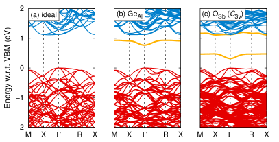
Note that equilibrium transition levels are distinct from electronic transition levels . While the former determine the equilibrium electron chemical potential at which a change in the charge state occurs, the latter are related to optical transitions. In the present work, we obtained electronic transition levels from band structure calculations of defect cells. Examples are shown in Fig. 4.
Binding energies for defect complexes are calculated according to
| (4) |
where the sum runs over the individual defects from which the complex is constructed. Note that changes with the electron chemical potential, since for both the complex and the individual defects depends on . According to Eq. (4) negative binding energies indicate a driving force for complex formation.
II.2 Defect structures
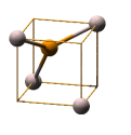
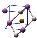
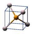
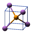
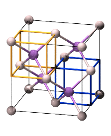
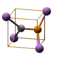
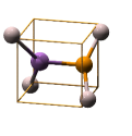
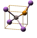
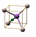
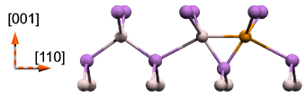
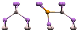
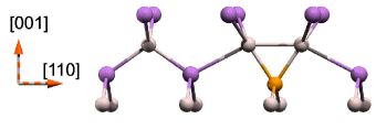
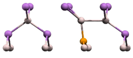
We consider C, Si, O, S, P, and H as potential impurities incorporated during the growth and include Ge, Sn, Se, and Te as possible compensating dopants. Figure 1 provides an overview of the defect configurations included in this work. To be specific, we took into account substitutional configurations with both tetrahedral () and trigonal () symmetry as well as four variations of cation-cation bonded (CCBDX) configurations that have been discussed in connection with DX-centers in III-V and II-VI semiconductors.Park and Chadi (1996); Du and Zhang (2005) (Additional tests were carried out for several distorted substitutional configurations, including molecular dynamics simulations in order to check for the existence of other relevant local minima, but did not reveal any further configurations of importance). With regard to interstitial configurations, we included tetrahedral (, ) and hexagonal sites () as well as several split-interstitial configurations oriented along and . The latter configurations were always observed to relax into a structure in which the bond between the impurity atom and its nearest neighbor is oriented slightly away from the direction [compare Fig. 1(h)]. In the literature, this distorted structure has been previously referred to as “bridge” interstitial, and for simplicity in the following we adopt this convention. We typically calculated formation energies for charge states between and , and where necessary also included charge states and .
We also investigated the formation of defect complexes of group IV and VI elements with aluminum vacancies and antimony antisites which are the two most important intrinsic defects.Åberg et al. (2008)
II.3 Computational details
Calculations were performed within density-functional theory (DFT) using the local density approximation (LDA) and the projector augmented wave method Blöchl (1994); Kresse and Joubert (1999) as implemented in the Vienna ab-initio simulation package. Kresse and Hafner (1993, 1994); Kresse and Furthmüller (1996a, b)
In our earlier study Åberg et al. (2008) of intrinsic defects in AlSb we employed a variety of supercell sizes in combination with a finite-size scaling procedure in order to mitigate the limitations of the supercell method. Given the large number of different elements, defect structures, and charge states considered in the present work, such a comprehensive approach is, however, beyond our present computational capabilities. We therefore carried out the majority of the calculations for 64-atom supercells, which based on the results of Ref. Åberg et al., 2008 implies that the error in our calculated formation energies due to the supercell approximation is still only on the order of 0.1 eV. For Brillouin-zone integrations we used a Monkhorst-Pack mesh. Monkhorst and Pack (1976) For a small set of configurations, we performed additional calculations using 216-atom cells (see Fig. 4) and a Monkhorst-Pack -point mesh to verify the viability of our 64-atom cell calculations. We used a plane-wave cutoff energy of 500 eV, which is imposed by the pseudo-potential for oxygen, but for the sake of consistency was used for all calculations. A Gaussian smearing with a width of was used to determine the occupation numbers. The ionic positions were optimized until the maximum force was below . For the charged defect calculations a homogeneous background charge was added to ensure charge neutrality of the entire cell.
For bulk AlSb we obtain a lattice constant of 6.12 Å in good agreement with the experimental room temperature value of 6.13 Å. The band gap is 1.12 eV, which is lower than the experimental room temperature value of 1.69 eV as expected for a LDA calculation. A more detailed overview of the bulk properties of Al, Sb, and AlSb that are obtained using the present computational parameters can be found in Ref. Åberg et al., 2008.
The underestimation of the band gap is a well-known deficiency of DFT within the LDA. In order to overcome this deficiency in Ref. Åberg et al., 2008 we have employed a post-mortem correction scheme which relies on a separation of valence and conduction band states. Analysis of the electronic structure of the defects in this work reveals that in many cases the defect induces electronic levels in the band gap, which renders the separation into valence, conduction or localized states highly unreliable. Since as a result the application of the correction scheme employed in Ref. Åberg et al., 2008 becomes ambiguous, we have decided to abstain from any band gap corrections in the present work. Instead all results are presented and discussed with respect to the calculated band gap, as done previously by Du. Du (2009) For reference we have, however, included the experimental band gap in Figs. 2, 5, and 6.
To compute the binding energies of defect complexes involving aluminum vacancies and antimony antisites, we used the defect formation energies obtained in Ref. Åberg et al., 2008 with for 64-atom cells and without band gap corrections
II.4 Lattice distortion and effect on charge carrier mobilities
Defects break the translational symmetry of an ideal crystal and therefore act as scattering centers for electrons and holes traveling through the crystal. The two most important contributions to the scattering cross section of a defect are related to the amount of charge localized at the defect (Coulomb scattering) and the lattice distortions that accompany defect relaxation. Since we are primarily interested in comparing defects that have identical absolute charge states (e.g., vs ), in the following we focus on the second contribution only. There are many different ways in which one can quantify lattice distortions. We have empirically found that a particularly useful measure is given by
| (5) |
where denotes the potential difference between the defective and ideal cells. This quantity includes not only ionic relaxations but also changes in the electronic charge distribution.
In Eq. (5) we use the potential and not —for example— the charge density difference. This choice is motivated by a full fledged computation of the scattering rates Lordi et al. (2010) based on Fermi’s golden rule for which one needs to evaluate matrix elements of the form .Chattopadhyay and Queisser (1981); Evans et al. (2005) In that study, Lordi et al. (2010) we find that reproduces very well the trends obtained from the scattering rate calculations based on Fermi’s golden rule across a wide range of extrinsic defects. Since the computation of is, however, orders of magnitude more efficient, in the following we use the relative scattering strength to assess the impact of defects on carrier transport. We note that this analysis does not differentiate between electron and hole scattering. It is, however, unusual that a given defect has a significantly different impact on electron and hole scattering. Lordi et al. (2010)
II.5 Self-consistent charge equilibration
In Refs. Åberg et al., 2008 and Erhart and Albe, 2008 we have described in detail a self-consistent scheme to determine the concentrations of defects and charge carriers as a function of temperature and chemical environment. Here, we only provide a brief summary of the most important equations. The concentrations of electrons, holes, and charged defects in a material are coupled to each other via the charge neutrality condition
| (6) |
where and are the electron and hole concentrations, respectively. They are given by
| (7) | ||||
| (8) |
where denotes the density of states, is the Fermi-Dirac distribution, is the electron chemical potential, VBM and CBM indicate the valence band maximum and the conduction band minimum, respectively. The concentrations of acceptors and donors, and , can be split into contributions due to intrinsic and extrinsic defects
| (9) |
The concentration of intrinsic acceptors (donors) is obtained by summing over all intrinsic defects with charge states (),
| (10) |
where is the unit of charge and the defect concentration is given by Eq. (1).
The concentrations of extrinsic acceptors and donors are given by expressions that are analogous to Eq. (10) but subject to the constraint that the total concentration of a given impurity or dopant is constant. A condition that can be easily achieved by proper normalization of the defect concentrations. The set of Eqs. (6–10) can be solved self-consistently using an iterative algorithm.
III Formation energies and defect structures
III.1 Group IV elements: C, Si, Ge, and Sn
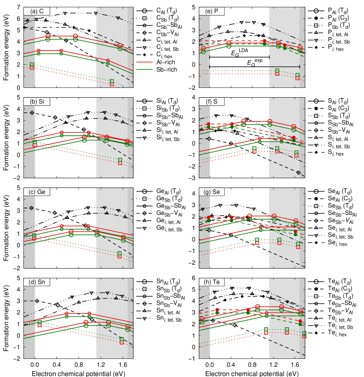
The formation energies of defects involving the first four group IV elements (C, Si, Ge, and Sn) are shown in Fig. 2(a–d). In all cases the most important configuration is the substitutional defect on an Sb-site, (=C, Si, Ge, or Sn). Regardless of the initial condition, we find the defects to relax into a configuration with symmetry. The defects occur predominantly in charge state and thus act as single acceptors. This observation is in agreement with Hall and resistivity measurements. Shaw (1962); Bennett et al. (2000); McCluskey et al. (2001)
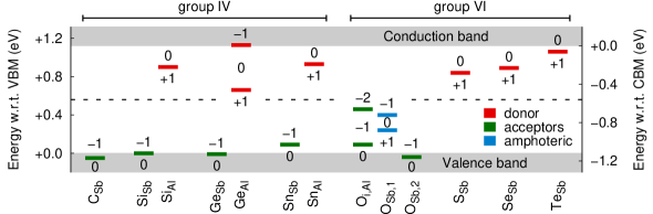
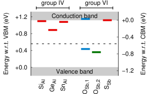
Within the error bars of our calculations the equilibrium transition levels for C, Si, and Ge coincide with the VBM whereas for Sn the equilibrium transition level is located 0.1 eV above the VBM (compare Fig. 3). In agreement with our calculations, shallow acceptor levels have been observed for Si by Bennett et al. Bennett et al. (2000) while C has been found to act an acceptor by McCluskey et al.. McCluskey et al. (2001) For defects, our calculations do not reveal any electronic states inside the band gap that could give rise to strong optical signatures.
For C the substitutional defect on an Al-site , which always adopts a local symmetry, is very high in energy and therefore should not occur in thermodynamic equilibrium. For Si, Ge, and Sn, however, this defect becomes increasingly more important. In fact in the case of Sn, the formation energies for substitutional defects on Al and Sb-sites are very similar. These results are consistent with the experiments by Shaw Shaw (1962) who observed that Sn can occupy both Al and Sb sites. For Si, Ge, and Sn the calculations predict to be a donor with a deep equilibrium transition level (compare Fig. 3). For Si, Ge, and Sn we also find electronic levels located inside the band gap. This is explicitly demonstrated for the case of in Fig. 4(b), which reveals a localized defect state approximately 0.24 eV below the CBM.
The similar formation energies of donors and acceptors gives rise to an interesting type of amphoteric behavior for Sn-doped AlSb. Usually this property is associated with a single defect type, which undergoes electronic (and usually also structural) changes as a function of charge state. In the case of AlSb:Sn, however, the amphoteric behavior is due to two different defects occupying two different lattice sites that possess opposite electronic characteristics. This leads to an intriguing opportunity for compensation doping that will be explored in Sec. V.4.
Regarding interstitial defects, both tetrahedral configurations and [Figs. 1(c) and 1(d)] are found to be local minima on the energy landscape with being slightly more stable. The hexagonal interstitial is a local minimum for C only, whereas it relaxes to the configuration for Si, Ge, and Sn. All interstitials are, however, significantly higher in energy than the most stable substitutional defects whence in thermodynamic equilibrium their concentrations should be negligible. Since the migration barriers for substitutional defects are, however, typically very large, it is possible that interstitial configurations play a role with respect to the diffusion of group IV elements.
We also considered defect complexes of group IV impurities with the intrinsic defects and . The formation energies for defects which act as acceptors are rather high due to the like charges of the two isolated defects. The complexes on the other hand display rather small formation energies that are typically less than 1 eV higher than the formation energy of the most stable configuration. These defects exhibit amphoteric behavior with the donor state dominating over the wider range of the band gap [also see Fig. 7(a)].
III.2 Group V elements: phosphorus
Phosphorus is included in the present work as a prototypical example for group V elements which are isoelectronic to Sb. The calculated formation energies are shown in Fig. 2(e) which shows that P prefers substitution on a Sb-site maintaining symmetry. is neutral throughout the band gap and thus does not introduce any transition levels inside the gap. All other possible configurations are much higher in energy.
III.3 Group VI elements: S, Se, and Te
Since oxygen behaves very different from the other group VI elements we first consider the less complex cases of S, Se, and Te. A detailed discussion of oxygen is given in the next section.
For S, Se, and Te the most stable defect configuration for electron chemical potentials over the widest range of the band gap is which possesses symmetry and acts as a donor [Figs. 2(f-h)]. The equilibrium transition levels for these defect are deep for all three elements (Fig. 3). While all interstitial configurations considered are local minima, they are always much higher in energy than the respective defect. Although there is supporting experimental evidence of the existence of shallow donor levels, Stirn and Becker (1966); Ahlburn and Ramdas (1968) it is firmly established that the ground-state of these donors for electron chemical potentials near the conduction band minimum is actually a DX-center Chadi and Chang (1988, 1989) associated with a deep level.Jost et al. (1994); Becla et al. (1995); Stallinga et al. (1995) As indicated in Sec. II.2, we have investigated a variety of possible DX-center structures. While we find several of these configurations to be local energy minima for charge state , their formation energies are always higher than the respective configurations in charge state as long as the electron chemical potential remains within the band gap. This behavior can be attributed to the LDA which in this instance fails to properly capture the energetics of localized vs delocalized defect states. A detailed discussion is, however, beyond the scope of this article and will be published elsewhere.
Defect complexes of with antisites for the group VI impurities show similar trends as in the case of the group IV impurities being about 1 eV higher than the isolated defects [see Fig. 7(c)]. In all cases, these complexes display donor character. In contrast to the group IV elements, however, the complexes have much lower formation energies resulting from the Coulombic interaction of the oppositely charged isolated defects. In fact, for electron chemical potentials in the upper half of the band gap, this mutual attraction renders the acceptor complex the most stable defect. The donor character of combined with the acceptor character of could allow for an interesting self-compensation effect. Since this would require that aluminum vacancies remain mobile down to very low temperatures () in order to achieve full equilibrium, such a scenario is, however, unlikely to occur in reality.
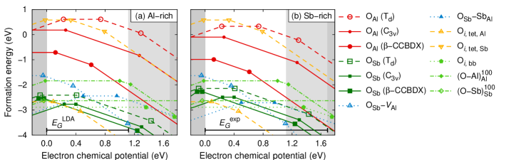
III.4 Group VI elements: oxygen
Oxygen behaves distinctly different from all the other elements considered so far , in that its interstitial configurations have very low formation energies and there is a multitude of different defect configurations which are all very close in energy (Fig. 5).
Over the widest range of the electron chemical potential, the most stable defect is the tetrahedral interstitial surrounded by Al atoms in charge state [Fig. 1(c)]. This acceptor defect displays transition levels () and () above the VBM (see Fig. 3).
For Al-rich conditions and electron chemical potentials in the lower half of the band gap, the lowest energy defect is an interstitial which assumes a bridgelike structure [Fig. 1(h)] and is indicated as in Fig. 5. It maintains the neutral charge state throughout the band gap. Very close to the VBM the defect emerges as the ground-state configuration. This defect adopts a configuration with symmetry and is associated with a pronounced lattice distortion [Fig. 1(a)]. It displays amphoteric characteristics with equilibrium transition levels () and () above the VBM. As shown in Figs. 3 and 4(c), it also introduces two electronic levels into the band gap that are located 0.45 eV above the VBM and right at the CBM, respectively.
For Sb-rich conditions and electron chemical potentials in the lower half of the band gap the defect complex which exhibits donor character prevail.
Finally, there are several other configurations with formation energies within about of the respective ground-state configurations. These include the split-interstitial [Fig. 1(g)], which is neutral throughout the band gap and electrically inactive, as well as the defect [Fig. 1(m)].
We observe a large number of oxygen configurations with very similar formation energies, and most of these defects lead to one or more deep equilibrium transition levels. Deep states induce defect-mediated recombination and/or trapping and thereby limit the lifetime of charge carriers. Oxygen incorporation is therefore very detrimental to the operation and energy resolution of a detector device.
III.5 Hydrogen
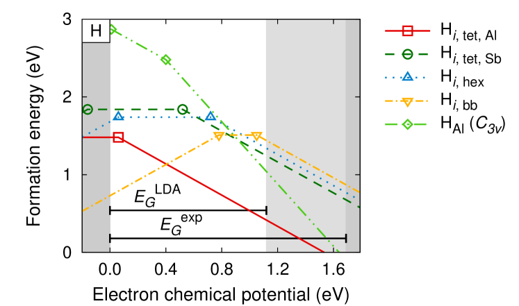
For hydrogen, we focused on interstitial configurations and considered both tetrahedral sites and the bridge bond configuration [Fig. 1(i)]. The results are shown in Fig. 6. For electron chemical potentials in the lower half of the band gap, the bridge bond configuration is the energetically most favorable one. It acts as a deep donor with an equilibrium transition level below the CBM. For electron chemical potentials in the upper half of the band gap, the defect prevails which behaves as an acceptor with an equilibrium transition level above the VBM. We also note that although the formation energies for and in the neutral charge state are virtually identical, the structures are nonetheless distinct.
III.6 Defect complexes

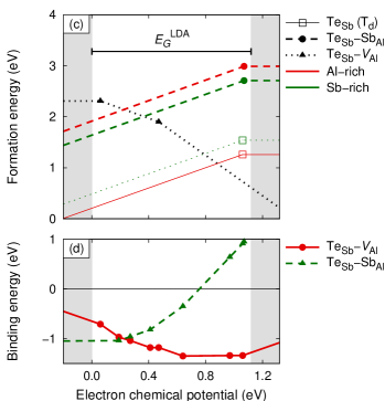
In this section, we consider the interaction of the two most important intrinsic defects Åberg et al. (2008) and with group IV and VI impurities. In the preceding sections, we have already seen that these defect complexes can have very low formation energies, in particular in the case of group VI elements, where for certain electron chemical potentials they are the most stable defect configuration.
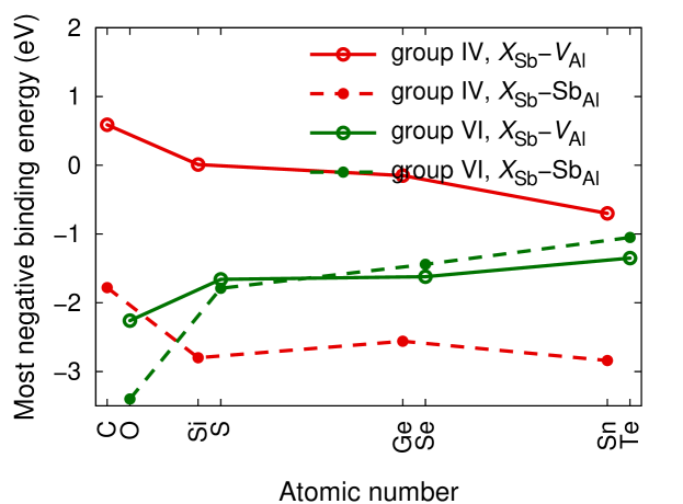
In Fig. 7, we show the binding energies and the respective formation energies of Sn and Te-complexes that are prototypical for group IV and VI elements, respectively. To illustrate the trends we show in Fig. 8 the most negative binding energies (indicating the strongest driving force for defect complex formation) for all group IV and VI impurities considered.
In the case of Sn, both types of complexes display strong binding for electron chemical potentials in the lower two-thirds of the band gap with binding energies as negative as for at the valence band maximum. On the other hand, for electron chemical potentials in the upper third of the band gap, the interaction is strongly repulsive. These trends hold for the other group IV elements as well with the exception of the complex which is never bound. In general, the vacancy complexes have high formation energies and act as acceptors, while the antisite complexes have rather low formation energies near the valence band edge and display mostly donor characteristics.
As exemplified by Te, the trends described above for prevails also for group VI elements. With respect to complexes with group VI impurities, we obtain binding energies which are consistently negative throughout the band gap. As discussed in Sec. III.3, the vacancy complexes act as acceptors, have relatively low formation energies, and are actually the most stable defect for electron chemical potentials near the CBM.
IV Relative scattering strengths
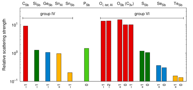
The relative carrier scattering strengths calculated using Eq. (5) for the most important intrinsic and extrinsic defects vary over several orders of magnitude as shown in Fig. 9. While the absolute values of the relative scattering strength bear no meaning, they still allow us to compare different extrinsic and intrinsic defects with respect to their impact on charge carrier mobility.Lordi et al. (2010)
Figure 9 clearly shows that oxygen induces by far the strongest carrier scattering and thus has the most detrimental impact on charge carrier mobilities, with carbon also showing a very high scattering strength. The relative scattering strengths for these impurities are about one order of magnitude larger than for the aluminum vacancy, which is the most detrimental intrinsic defect.
For the elements within the same group of the periodic table, the scattering strength generally decreases with increasing atomic number. This effect is owed to the diminishing size mismatch between the impurity atom and Sb, for which most impurities substitute, leading to decreased lattice distortion upon substitution. As a result, the elements that have the least negative effect on carrier mobility, are Sn, Se, and particularly Te. In fact, many of the substitutional impurities scatter carriers less strongly than the intrinsic defects. These elements are therefore excellent candidates for doping the material in order to achieve carrier compensation with minimal impact on mobility, an opportunity that is explored in the following section.
V Charge carrier concentrations
In the previous sections we have determined the formation energies of a wide range of extrinsic defects and discussed which of them act as donors or acceptors. Furthermore, we have obtained their relative scattering rates, which enabled us to identify the defects which are, respectively, the least and most detrimental to the electron and hole mobilities in the material. Now, we are in a position to combine these data to predict net charge carrier concentrations and to determine conditions for obtaining optimal material. For radiation detection, the objective is to obtain a material which features maximal charge carrier mobilities, which requires small scattering rates, and very high resistivity, which requires low net charge carrier concentrations.
In the analysis that follows, we consider four important cases. First, we analyze the pure material (containing only intrinsic defects). Then, we include in our model unintentional impurities from the growth process, followed by analysis of carrier compensation with intentional Te doping. Finally, we consider the case of Sn doping, which exhibits unique behavior due to its amphoteric character.
V.1 Pure material
In Ref. Åberg et al., 2008, we employed the self-consistent charge equilibration scheme described in Sec. II.5 to determine the concentrations of intrinsic defects and charge carriers in pure AlSb (no impurities) using defect formation energies calculated from DFT, which had been corrected for the band gap error. As discussed in Sec. II.3, in the present work we did not employ any such corrections. Before we can apply the self-consistent charge equilibration scheme to study the behavior of extrinsically doped AlSb, we therefore have to discuss to which extent the band gap error influences the results. According to Eq. (7) the intrinsic electron and hole concentrations depend exponentially on the band gap. To be consistent with the calculations discussed above, we now have to use the LDA band gap and the corresponding formation energies for the intrinsic defects. The absolute carrier concentrations are therefore no longer comparable to our calculations in Ref. Åberg et al., 2008. For the present purpose, we are, however, interested not in absolute carrier concentrations but in net charge carrier concentrations, i.e. the difference between the concentrations of electron and holes,
| (11) |
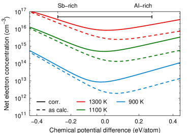
The impact of the band gap error on is not immediately obvious. In Fig. 10, we therefore compare the net electron concentrations for pure AlSb using as-calculated formation energies as well as formation energies, which have been corrected for the band gap error. We find that while the actual values deviate somewhat, the conduction type ( vs ), chemical potential dependence, and the order of magnitude of are very similar. This finding enables us to use the as-calculated formation energies to compute net charge carrier concentrations for AlSb with extrinsic defects. Figure 10 also shows that pure AlSb exhibits -type behavior over the entire range of the chemical potential difference. In contrast, as-grown AlSb has been found to exhibit -type conductivity. In the following section, we show that this apparent discrepancy is caused by the accidental incorporation of impurities during growth.
V.2 Unintentional background doping
In the experimental growth process, certain impurities are impossible to avoid. In particular this includes oxygen and carbon.McCluskey et al. (2001); Erhart et al. (a) Oxygen can be incorporated from the gas phase or the components of the growth chamber and is also present in the raw starting materials. Carbon enters because graphite susceptors are used to heat the melt.111Additional impurities have been measured in high-purity samples using secondary ion mass spectroscopy including S, Si, and P. These impurities can, however, be fairly well controlled experimentally and according to our calculations in Sec. IV are also not as detrimental for carrier mobility as C and O. Using a highly optimized growth process, it is possible to reduce the concentration of oxygen to about and the concentration of carbon to about .Erhart et al. (a)
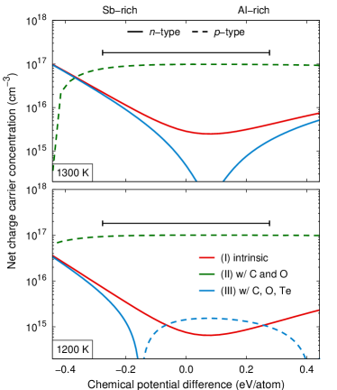
In Fig. 11, we show the net charge carrier concentrations for AlSb with and . In fact, these concentrations cause the conductivity to switch from -type to -type, which resolves the apparent discrepancy between theory and experiment mentioned above. The inversion of the conductivity-type is indeed expected since in Sec. III both of these impurities have been identified as acceptors.
V.3 Compensation with Te
Since the background doping by C and O renders the material -type, compensation requires addition of donor ions. To simultaneously achieve high carrier mobilities and low net carrier concentrations, the dopant should possess a scattering potential which is as small as possible. According to Figs. 2 and 9 Te is an ideal candidate based on these criteria. In Fig. 11 we show the effect of adding Te at a concentration of to AlSb containing C and O impurities. We find that by using Te doping in this concentration range the net charge carrier concentration can be tuned very efficiently. The net carrier concentration changes as a function of the chemical potential difference between Al and Sb, with a minimum close to the Sb-rich limit (typical annealing condition). Intentional doping with Te therefore enables us to compensate the background doping due to C and O impurities while minimizing the detrimental impact on the carrier mobilities. In fact, using these data as a guidance for the experimental growth process led to a dramatic improvement of the material for radiation detection, which is reported elsewhere. Erhart et al. (a)
V.4 Ambipolar doping with Sn
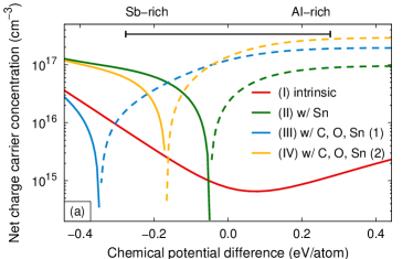
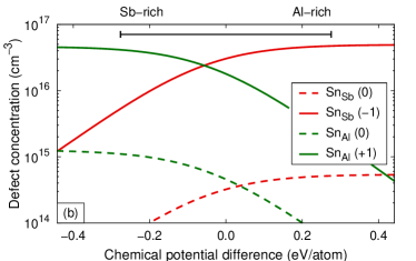
According to Fig. 2, Sn can be incorporated both on the Sb and the Al sublattice, which gives rise to acceptor and donor-type defects, respectively. Also, Fig. 9 shows that both of these defects are weak scatterers compared to the aluminum vacancy. Figure 12(a) illustrates the effect of Sn on the net charge carrier concentration. In thermodynamic equilibrium and for a Sn concentration of about , the material is -type if grown under Sb-rich conditions and -type if grown under Al-rich conditions [case II in Fig. 12(a)]. In the presence of C and O impurities this behavior is retained although the transition point is shifted toward Sb-rich conditions [case C in Fig. 12(a)]. By increasing the Sn concentration the minimum in can be shifted back toward the impurity-free case [case IV in Fig. 12(a)]. Figure 12(b) reveals that the origin of this behavior is the subtle equilibrium between and defects, which act as acceptors and donors, respectively.
We suggest that this intriguing property of Sn-doped AlSb can be exploited to achieve self-compensation. In a typical experiment, an AlSb single crystal is grown under Al-rich conditions close to the melting point of 1330 K. The growth process is sufficiently slow to assume that we are near thermodynamic equilibrium, which implies that the vast majority of Sn occupies Sb-sites. The growth step is usually followed by a high-temperature anneal at about 1200 K under Sb-rich conditions. This inversion of chemical conditions leads to a strong driving force for redistributing Sn from the Sb to the Al sublattice. This conversion can be mediated by aluminum vacancies which at this temperature are both very mobile Erhart et al. (b) and exist in high concentrations.Åberg et al. (2008) By carefully controlling the annealing time it should thus be possible to achieve a ratio close to one. At this point the material would be perfectly compensated due to the opposing effects of and defects. Due to the moderate scattering strength of Sn-related defects such a material would exhibit high carrier mobilities in conjunction with high resistivity, as needed for the radiation detection applications.
VI Conclusions
In this work we have investigated the thermodynamic and electronic properties of group IV and group VI impurities as well as P and H in AlSb using density-functional theory calculations. First, we computed the formation energies for a wide range of possible defect configurations and charge states to identify the most important defect configurations, their electronic characteristics, and their equilibrium and electronic transition levels. We found that C, Si, and Ge preferentially substitute for Sb, act as acceptors and exhibit shallow transition levels. Sn, however, can substitute for Sb and Al and displays amphoteric behavior.
With regard to group VI elements, S, Se, and Te substitute for Sb and have deep donor levels. Oxygen in contrast can be incorporated in several different configurations that display a variety of electronic characteristics and transition levels, predominantly of the acceptor type. For the widest range of electron chemical potentials a tetrahedral interstitial configuration is the lowest in energy.
Phosphorus substitutes for Sb and is electrically inactive while H is incorporated on interstitial sites and can act as acceptor or donor depending on conditions.
With respect to defect complexes, our calculations show that group IV elements bind to both aluminum vacancies () and Sb antisites () for electron chemical potentials in the lower two-thirds of the band gap. (The complex is an exception and is never bound). The vacancy complexes have high formation energies and act as acceptors while the antisite complexes have rather low formation energies near the valence band edge and display mostly donor characteristics. Similar trends hold for group VI elements but in this case the vacancy complexes show negative binding energies over the entire range of the band gap. In addition, the formation energies of antisite complexes are very low near the conduction band edge, which for S, Se, and Te renders them even more stable than the individual defects in a small range of electron chemical potentials in the upper third of the band gap.
To characterize the effect of different impurities on the charge carrier mobilities, we calculated relative scattering strengths. This analysis revealed that C and O have by far the most detrimental impact on carrier transport. The scattering strengths for Sn, Se, and Te, however, are similar or even smaller than for the most important intrinsic defects. Tellurium, in particular, is therefore an excellent candidate for compensation doping the material.
The interplay of electronic characteristics and impurity concentrations was investigated using a self-consistent charge equilibration scheme that allowed us to compute net charge carrier concentrations. While pure material was found to exhibit -type conductivity, the incorporation of C and O leads to -type material. This observation is consistent with experimental measurements which show -type conductivity in as-grown samples which contain an unintentional background concentration of C and O impurities. Our calculations furthermore revealed how Te can be used to compensate these impurities in order to achieve minimal net charge carrier concentrations. Finally, we discussed how the amphoteric character of Sn could be used to achieve self-compensated material via controlled annealing.
Acknowledgements.
This work performed under the auspices of the U.S. Department of Energy by Lawrence Livermore National Laboratory under Contract No. DE-AC52-07NA27344 with support from the Laboratory Directed Research and Development Program and from the National Nuclear Security Administration Office of Nonproliferation Research and Development (NA-22).References
- Owens (2006) A. Owens, J. Synchrotron Radiat. 13, 143 (2006).
- Luke and Amman (2007) P. N. Luke and M. Amman, IEEE Trans. Nucl. Sci. 54, 834 (2007).
- Mayer (1967) J. W. Mayer, in Semiconductor Detectors, edited by A. Coche and G. Bertolini (North Holland Publishing Co., Amsterdam, 1967), Chap. 5.
- Armantrout et al. (1977) G. A. Armantrout, S. P. Swierkowski, J. W. Sherohman, and J. H. Lee, IEEE Trans. Nucl. Sci. 24, 121 (1977).
- Kutny et al. (2001) V. E. Kutny, A. V. Rybka, A. S. Abyzov, L. N. Davydov, V. K. Komar, M. S. Rowland, and C. F. Smith, Nucl. Instrum. Methods Phys. Res. A 458, 448 (2001).
- Knoll (2000) G. F. Knoll, Radiation Detection and Measurement (Wiley, 2000), Chap. 12.
- Åberg et al. (2008) D. Åberg, P. Erhart, A. J. Williamson, and V. Lordi, Phys. Rev. B 77, 165206 (2008).
- Lordi et al. (2010) V. Lordi, P. Erhart, and D. Åberg Phys. Rev. B 81, 235204 (2010).
- Zhang and Northrup (1991) S. B. Zhang and J. E. Northrup, Phys. Rev. Lett. 67, 2339 (1991).
- Du (2009) M.-H. Du, Phys. Rev. B 79, 045207 (2009).
- Du and Zhang (2005) M. H. Du and S. B. Zhang, Phys. Rev. B 72, 075210 (2005).
- Park and Chadi (1996) C. H. Park and D. J. Chadi, Phys. Rev. B 54, R14246 (1996).
- Blöchl (1994) P. E. Blöchl, Phys. Rev. B 50, 17953 (1994).
- Kresse and Joubert (1999) G. Kresse and D. Joubert, Phys. Rev. B 59, 1758 (1999).
- Kresse and Hafner (1993) G. Kresse and J. Hafner, Phys. Rev. B 47, 558 (1993).
- Kresse and Hafner (1994) G. Kresse and J. Hafner, Phys. Rev. B 49, 14251 (1994).
- Kresse and Furthmüller (1996a) G. Kresse and J. Furthmüller, Phys. Rev. B 54, 11169 (1996a).
- Kresse and Furthmüller (1996b) G. Kresse and J. Furthmüller, Comput. Mater. Sci. 6, 15 (1996b).
- Monkhorst and Pack (1976) H. J. Monkhorst and J. D. Pack, Phys. Rev. B 13, 5188 (1976).
- Chattopadhyay and Queisser (1981) D. Chattopadhyay and H. J. Queisser, Rev. Mod. Phys. 53, 745 (1981).
- Evans et al. (2005) M. H. Evans, X.-G. Zhang, J. D. Joannopoulos, and S. T. Pantelides, Phys. Rev. Lett. 95, 106802 (2005).
- Erhart and Albe (2008) P. Erhart and K. Albe, J. Appl. Phys. 104, 044315 (2008).
- Shaw (1962) D. Shaw, Proc. Phys. Soc. 80, 161 (1962).
- Bennett et al. (2000) B. R. Bennet, W. J. Moore, M. J. Yang, and B. V. Shanabrook, J. Appl. Phys. 87, 7876 (2000).
- McCluskey et al. (2001) M. D. McCluskey, E. E. Haller, and P. Becla, Phys. Rev. B 65, 045201 (2001).
- Stirn and Becker (1966) R. J. Stirn and R. M. Becker, Phys. Rev. 141, 621 (1966).
- Ahlburn and Ramdas (1968) B. T. Ahlburn and A. K. Ramdas, Phys. Rev. 167, 717 (1968).
- Chadi and Chang (1988) D. J. Chadi and K. J. Chang, Phys. Rev. Lett. 61, 873 (1988).
- Chadi and Chang (1989) D. J. Chadi and K. J. Chang, Appl. Phys. Lett. 55, 575 (1989).
- Jost et al. (1994) W. Jost, M. Kunzer, U. Kaufmann, and H. Bender, Phys. Rev. B 50, 4341 (1994).
- Becla et al. (1995) P. Becla, A. Witt, J. Lagowski, and W. Walukiewicz, Appl. Phys. Lett. 67, 395 (1995).
- Stallinga et al. (1995) P. Stallinga, W. Walukiewicz, E. R. Weber, P. Becla, and J. Lagowski, Phys. Rev. B 52, R8609 (1995).
- Erhart et al. (a) P. Erhart, D. Åberg, B. W. Sturm, K.-J. Wu, and V. Lordi, submitted.
- Erhart et al. (b) P. Erhart, D. Åberg, and V. Lordi, unpublished.