Intrinsic point defects in aluminum antimonide
Abstract
Calculations within density functional theory on the basis of the local density approximation are carried out to study the properties of intrinsic point defects in aluminum antimonide. Special care is taken to address finite-size effects, band gap error, and symmetry reduction in the defect structures. The correction of the band gap is based on a set of GW calculations. The most important defects are identified to be the aluminum interstitial , the antimony antisites and , and the aluminum vacancy . The intrinsic defect and charge carrier concentrations in the impurity-free material are calculated by self-consistently solving the charge neutrality equation. The impurity-free material is found to be n-type conducting at finite temperatures.
pacs:
61.72.J-, 61.72.Bb, 61.82.Fk, 71.15.MbI Introduction
Aluminum antimonide is receiving much renewed interest for applications ranging from ionizing radiation detection to microelectronics to optoelectronics. For gamma radiation detection, AlSb is particularly promising as a novel material enabling high energy-resolution detection at room temperature due to its indirect band gap of 1.6 eV, the high atomic number of Sb, and the potentially high electron and hole mobilities of up to several hundred cm2 V-1 s-1 at room temperature.Armantrout et al. (1977); Owens (2006) Improved materials for high resolution, room temperature gamma radiation detectors are critically needed for applications in nuclear nonproliferation and monitoring, homeland security, and also medical and space imaging applications. Such detectors operate by counting the number of electron-hole pairs created in the semiconductor upon interaction with a gamma ray. Thus, a small band gap is generally desired to maximize the number of generated carriers, increasing the signal and reducing the shot noise. However, if the band gap is too small, excess thermal noise is generated from carriers thermally excited across the gap. At room temperature, a gap of 1.6 eV is nearly optimal. In a similar vein, low intrinsic carrier concentrations in the material may be desired to reduce the background signal, another noise source. Furthermore, high energy resolution (counting statistics) is achieved by maximizing the efficiency of charge collection, which requires high carrier mobilities and long carrier lifetimes. An indirect band gap can be advantageous for maximizing carrier lifetimes by quenching radiative recombination. Finally, high atomic number in the material is desired to increase the stopping power for high energy radiation, reducing the required size of the device. Presently, the purity of large single-crystal growths of AlSb limits its performance for radiation detection application.
In microelectronics, AlSb and related alloys containing In, are finding use in advanced field-effect transistor designs that promise higher switching speeds and lower power consumption compared to silicon devices.Tuttle and Kroemer (1987); Ashley et al. (2007) The material has also found use in high current density, high speed resonant tunnel diodes.Soderstrom et al. (1991) In optoelectronics, thin films of AlSb are being used in active regions and superlattice structures for claddings in novel type-II infrared cascade lasers.Canedy et al. (2006, 2007); Devenson et al. (2007) Such lasers, emitting wavelengths around 3–4.3 m, find application, for example, in remote atmospheric chemical sensing. Aluminum antimonide is particularly interesting in these applications because it has a large 2.1 eV conduction band offset with InAs, which often comprises the other key component in the active layers of these devices.
In the present work, we present a careful analysis of the thermodynamic and electronic properties of intrinsic point defects in AlSb, since the electronic and transport properties of the material can be degraded by detrimental defects. The main goals of this study are to identify the most important intrinsic point defects and to establish the concentrations of defects and charge carriers in thermal equilibrium. This work is part of a larger effort to understand the fundamental microscopic limits of performance of this and other semiconductor materials. Future work will focus on extrinsic impurities in the material, as well as the implications on carrier transport properties.
Our major findings in this work are that the dominant native defects in AlSb are aluminum interstitials, antimony antisites, and aluminum vacancies, dependent on chemical environment and doping. The equilibrium concentration of total native defects near the melting temperature is found to be in the to cm-3 range, while at lower temperatures, concentrations down to cm-3 or lower are expected. The electron chemical potential in pure material is near the middle of the band gap, however the material tends naturally to be slightly n-type doped by charged aluminum interstitials.
The paper is organized as follows. In Sec. II we review the thermodynamic formalism we use to derive defect formation energies and concentrations from first principles calculations, and describe the computational details which underlie the present work. In Sec. III we report the relaxed defect geometries, defect formation energies, and the charge carrier and defect concentrations, which are obtained by self-consistently solving the charge neutrality condition. Finally, in Sec. IV we discuss the intrinsic limitations of AlSb on the basis of our results and the relation to experimental data. The Appendix contains a brief derivation of the band gap correction scheme utilized in the present work.
II Methodology
II.1 Point defect thermodynamics
A material in thermodynamic equilibrium must contain a certain number of point defects at finite temperature, due to entropy. The temperature dependence of the equilibrium defect concentration can be shown to obey the following relation Allnatt and Lidiard (2003)
| (1) |
where denotes the concentration of possible defect sites, is Boltzmann’s constant, and is absolute temperature. The Gibbs energy of defect formation, , can be split into three distinct terms
| (2) |
The formation entropy, , is typically on the order of , so the entropy term hardly exceeds 0.1 eV even at elevated temperatures. In some cases, entropic effects could play a role in stabilizing a defect at high temperatures when the enthalpy differences are small. We do not explicitly treat this effect here, but point out cases in our results where it may be important. The formation volume, , describes the pressure dependence of the Gibbs energy of formation and is typically some small fraction of the atomic volume, so it can be neglected at ordinary pressures. The most important contribution is the defect formation energy, . In the following, we therefore focus on the formation energy and for simplicity ignore both the entropy and volume terms.
For a binary compound the formation energy for a defect in charge state is given byQian et al. (1988); Zhang and Northrup (1991)
| (3) |
where is the total energy of the system containing the defect, denotes the number of atoms of type , is the chemical potential of component in its reference state, and we have written the terms using explicit labels for AlSb. Neglecting entropic contributions, the chemical potentials of the reference phases can be replaced by their cohesive energies at 0 K. The formation energy depends on the chemical environment via the parameter , which describes the variation of the chemical potentials under different conditions. The range of is constrained by the formation energy of AlSb by , where for the present convention and correspond to Al and Sb-rich conditions, respectively. Finally, the formation energy also depends on the electron chemical potential, , which is measured with respect to the valence band maximum, .
II.2 Computational details
The energy terms in Eq. (3) were calculated using density functional theory (DFT) carried out in the local density approximation (LDA) using the Vienna Ab-initio Simulation Package (vasp) Kresse and Hafner (1993, 1994); Kresse and Furthmüller (1996a, b) and the projector augmented-wave (PAW) method.Blöchl (1994); Kresse and Joubert (1999) Defect formation energies were obtained using supercells of various size containing 32, 64, 128, and 216 atoms. Extrapolation was used to account for finite-size effects as described in detail in Sec. II.3. Brillouin zone integrations were performed with -point grids generated using the Monkhorst-Pack scheme.Monkhorst and Pack (1976) For the 32 and 64-atom cells, a non-shifted mesh was used, while for the 128-atom cell, a shifted grid was used. For the 216-atom cell, a non-shifted mesh was constructed. The plane wave cutoff energy was set to 300 eV and Gaussian smearing with a width of 0.1 eV was used to determine the occupation numbers. For charged defect calculations, a homogeneous background charge was employed (by omitting the term in the potential) to ensure charge neutrality of the entire cell.
Atomic relaxations were performed to determine the equilibrium structures of the defects, with ionic forces converged to 20 meV/Å and all calculations performed at the theoretical equilibrium volume. Relaxations from various randomized initial configurations were performed to avoid high-symmetry local energy minima in the structures.
II.3 Finite-size corrections
In the supercell approximation there are spurious interactions between defects and their periodic images which lead to systematic errors.Zhao et al. (2004); Erhart et al. (2006) For neutral defects the leading error is due to elastic interactions, which cause an overestimation of the formation energy. The strain energy of a point-like inclusion can be derived from linear elasticity theory and can be shown to fall off roughly with , where is the distance between periodic images. Grecu and Dederichs (1971); Dederichs and Pollmann (1972) Therefore, the formation energy in the dilute limit () can be obtained by finite-size scaling with , which removes the elastic strain component.
Makov and Payne considered the convergence of the energy of charged systems in periodic systems and proposed a correction on the basis of a multipole expansion.Makov and Payne (1995) The leading term corresponds to the monopole-monopole interaction and scales with . This term can be analytically determined if the static dielectric constant of the medium, , and the Madelung constant of the Bravais lattice of the supercell, , are known:Makov and Payne (1995); Lento et al. (2002)
| (4) |
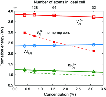
The next higher order term in the expansion is the monopole-quadrupole interaction which scales as . Even higher order terms (, ) are usually small and therefore neglected. In the present work, we have applied the monopole-monopole correction term using the experimental value for the static dielectric constant (). Then, since both the elastic and the monopole-quadrupole interactions scale with , we employed finite-size scaling with to correct for these terms. This extrapolation scheme gave very small extrapolation errors as shown in Tables 2 and 3. The results of the finite-size scaling procedure are illustrated in Fig. 1 for the most important defects. Figure 1 clearly illustrates the effect of the monopole-monopole correction term which tremendously reduces the variation between the supercells. The remaining higher-order variations are very well captured by the finite-size scaling. In addition, the potential alignment correction described in Ref. Zhao et al., 2004 is implicitly taken into account by our extrapolation scheme.Erhart and Albe (2007)
II.4 Band gap corrections
The underestimation of the band gap (by the LDA) affects the formation energies, as discussed in detail in the Appendix. A simple correction scheme based on the band energy has been proposed by Persson et al. Persson et al. (2005) and is further motivated in the Appendix. The correction amounts to the following term which is added to the as-calculated formation energies:
| (5) |
where and are shifts of the valence and conduction band edges, respectively, to correct the band gap, while and are the number of unoccupied valence and occupied conduction band states, respectively.
|
|
|
| Charge state | |||||
|---|---|---|---|---|---|
| † | stable | † | † | † | |
| † | † | stable | stable | stable | |
| stable | stable | stable | stable | ||
| † | † | ||||
| stable | stable | stable | stable | stable | |
| stable∗ | stable∗ | stable∗ | |||
| stable | stable | stable | stable | stable |
†Relaxations starting from the idealized positions maintained the initial symmetry, but when started from
randomized positions, relaxed to the indicated structure
∗Split interstitial displaced along from ideal position
In the present work the energy offsets and were obtained from G0W0 calculations Hedin (1965) within the single plasmon-pole model as implemented in abinit. Gonze et al. (2002); Goedecker (1997); abi Non-selfconsistent G0W0 calculations were employed to properly refer the quasiparticle energies to the same potential zero as the LDA eigenvalues. Fritz-Haber-Institute norm-conserving pseudopotentials Fuchs and Scheffler (1999) in the Troullier-Martins scheme Troullier and Martins (1991) were used with a cutoff energy of 15 Hartree (Ha). The other relevant cutoff energies used in the calculation were 5 Ha for the self-energy wave functions, 6 Ha for the exchange part of the self-energy, and 6 Ha for the screening matrix. The number of bands in the self-energy and screening matrix calculations were 100 and 150, respectively.
In Table 2 we report both the as-calculated formation energies (including finite-size scaling) and the band gap-corrected formation energies. The correction terms can be reproduced using the values for and included in the table. Note that we extracted and values only for the most important defects for which an unambiguous distinction between valence and conduction band states was possible. A direct comparison of the as-calculated and band gap-corrected values is shown in Fig. 3, and discussed later in Sec. III.3.
The defect concentrations calculated in Sec. III.4 were obtained using the band gap-corrected formation energies and the GW band gap.
III Results
III.1 Bulk properties
As described in Sec. II.1 and evident in Eq. (3), the determination of defect formation energies requires that we also calculate bulk properties of the solid and its constituents in reference states. The reference states for Al and Sb are face-centered cubic (fcc) and rhombohedral solids, respectively.
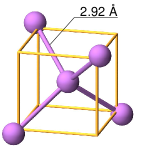
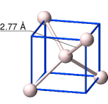
For fcc aluminum, we obtain a lattice constant of and a cohesive energy of which compare reasonably well with the experimental values of (room temperature)Massalski (1986) and .James and Lord (1992) The underestimation of the lattice constant and the overestimation of the cohesive energy are typical for LDA calculations. Antimony has a rhombohedral groundstate structure (Rmh, space group no. 166, Strukturbericht symbol A7) for which the DFT calculations yield a lattice constant of and a rhombohedral angle of (experimental values: and , Ref. [Massalski, 1986]) and a cohesive energy of (experimental value: , Ref. [James and Lord, 1992]).
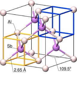
At ambient conditions bulk aluminum antimonide adopts the zinc-blende structure (F3m, space group no. 216, Strukturbericht symbol B3). The DFT calculated lattice constant is 6.12 Å in good agreement with the experimental value of 6.13 Å (300 K). The DFT calculations furthermore yield a formation enthalpy of (experimental value: ). The direct and indirect band gaps are calculated as 1.53 and 1.12 eV, respectively, while the experimental values are 2.30 and 1.62 eV at 300 K.Madelung (2004)
From the GW calculations, we obtain direct and indirect band gaps of 2.31 and 1.64 eV, respectively, in excellent agreement with the experimental values cited above. The shifts of the valence and conduction band edges showed small variations with -vector, so we calculated and which appear in Eq. (5) as weighted averages over all -points included in the calculations. The shifts thus obtained are and .
III.2 Defect structures
We considered all possible native defects in AlSb up to split interstitials. In total, this amounts to 18 different defects (two vacancies, two antisite defects, four tetrahedral interstitials, two hexagonal interstitials, and eight split interstitials), not all of which are stable. For each defect, we investigated a series of charge states, generally from to , as appropriate. Defect complexes were not considered.
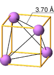
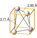
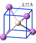
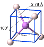
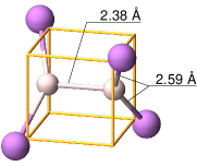
Vacancies. In the ideal zinc-blende structure, both Al and Sb sites possess tetrahedral symmetry with nearest neighbor distance of 2.65 Å. If one removes a single atom and allows the system to relax from randomized positions, the aluminum vacancy maintains the symmetry for all relevant charge states and the surrounding antimony ions relax inward by 0.36 Å (for ) to 0.38 Å (for ) [see for example Fig. 2(a)]. This behavior is typical of cation vacancies in III-V and II-VI zinc-blende semiconductors, where a dimerization transformation of the atoms surrounding the vacancy is generally not energetically favorable.Chadi (2003) In contrast, the antimony vacancy exhibits a Jahn-Teller distortion to a local tetragonal symmetry for all but the positive charge states. The relaxed configuration for is shown in Fig. 2(b) representatively, also indicating the pairing of Al atoms in the first neighbor shell of the vacancy.
Antisites. Both the and antisite defects maintain the symmetry for all relevant charge states. In the case of , the surrounding aluminum ions relax inwards, while for the nearest neighbor antimony ions relax outwards [compare Figures 2(c) and (d)]. These relaxations occur as expected based on the atomic radii.
Tetrahedral interstitials. In the zinc-blende structure there are two distinct tetrahedral sites: one centered on an Al tetrahedron (4d site) and one centered on an Sb tetrahedron (4b site). Thus, there are four possible types of tetrahedral interstitials: and on the 4d site; and on the 4b site.
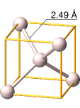
Both kinds of tetrahedral aluminum interstitials (, ) maintain the symmetry after relaxation, with the neighboring ions relaxing outwards as shown in Figs. 2(f) and (g). The configuration is unstable in all but the charge state; in all other charge states, the interstitial atom relaxes either onto a hexagonal site or forms a split interstitial. Conversely, is stable in all of its charge states, but does exhibit Jahn-Teller distortions as illustrated in Fig. 2(h).
Hexagonal interstitials. The hexagonal interstitial is located at Wyckoff position 16e. The aluminum hexagonal interstitial was found to be unstable for all charge states, with the Al atom observed to relax into the configuration even when starting from ideal positions. For the antimony hexagonal interstitial , the charge state was found to relax directly into the position, whereas for charge states and the interstitial atom remained in the hexagonal site. The other charge states when perturbed from the ideal position relax into the split interstitial, described below.
Split interstitials. Split interstitial configurations, in which two atoms share one atom site, have been extensively discussed in the literature for the zinc-blende structure. Baraff and Schlüter (1985); Zhang and Northrup (1991); Chadi (1992); Laasonen et al. (1992); Schick et al. (2002); Zollo and Nieminen (2003); El-Mellouhi and Mousseau (2005) We have carried out an exhaustive exploration of the structures of these defects in AlSb. The following cases were considered: two Al atoms oriented along sharing one Al site [], the same atoms but oriented along [], one Al atom and one Sb atom oriented along sharing one Al site [], and the same combination of atoms oriented along []. Four more configurations are obtained corresponding to the same combinations above, but sharing an Sb site.
Most of these configurations actually are found to be unstable with respect to other interstitial configurations. The results of these calculations are summarized in Table 1, which shows which configurations were found to be stable and which ones were unstable or only conditionally stable with respect to alternative interstitial configurations. In certain cases, a structure relaxed starting from the ideal atomic coordinates maintained the starting symmetry after relaxation, but when started from randomized coordinates, the structure relaxed to a different configuration; these cases are indicated in Table 1 by listing both final configurations. The cases simply marked stable (single entry ‘stable’) in Table 1 relaxed to the ideal symmetry configuration for all starting configurations.
For completeness, we note that the split interstitial in charge states , , and is displaced along from the ideal position, such that the Sb interstitial is located in between two regular Sb atoms along the direction.
III.3 Formation energies
| Defect | as-calc. | corr. | |||||
|---|---|---|---|---|---|---|---|
| Al-rich | Sb-rich | Al-rich | Sb-rich | ||||
| Defect | Al-rich | Sb-rich | ||
|---|---|---|---|---|
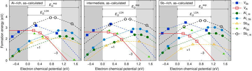
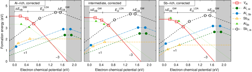
The defect formation energies calculated using Eq. (3) for Al-rich and Sb-rich conditions and an electron chemical potential at the valence band maximum are given in Tables 2 and 3. The formation energies for the dominant defects (lowest ) are shown as a function of the electron chemical potential in Fig. 3.
Figure 3 also illustrates the effect of the band gap correction described in Sec. II.4. In the top row we show the formation energies after the finite-size scaling procedure was applied but without the band gap correction. The bottom row shows the results including the band gap corrections. It is apparent that as the band gap correction is applied donor and acceptor levels track the conduction and valence band edges, respectively. This feature is independent of the relative values of and in Eq. (5).
It is interesting to compare the band gap-corrected formation energies in the bottom panel of Fig. 3 with those in the top panel if the band gap is simply extended to the experimental value by shifting the conduction band upwards. Considerable differences are observed between the two cases, with the values corrected using the scheme presented here being more consistent. In fact, we observe that, qualitatively, the results obtained by applying no correction at all are more similar to the corrected results than what is obtained by assigning the band gap error fully to the conduction band.Foster et al. (2001); Kohan et al. (2000) Furthermore, a correction procedure often suggested in the literatureSchick et al. (2002) to simply shift the ionization energies of donor-like defects to track the conduction band minimum (implicitly leaving the ionization energies of acceptor-like defects tracking the valence band maximum), without accounting for the occupation of states, does not properly correct the errors in the formation energies. The scheme employed here results in an identical shift of the ionization energies, but also corrects the errors in the formation energies.However, we note that this scheme still neglects both level relaxations and changes in the double counting term.
We believe the method presented here is the most consistent way to address the LDA band gap problem, with the use of GW calculations providing a first principles approach to calculating the correction terms. We find that neglecting to include the band gap correction terms in the formation energies leads to significant errors in the prediction of defect concentrations and which defects are dominant.
III.4 Defect and charge carrier concentrations
With the formation energies known, the equilibrium defect concentrations for a given chemical potential difference can be calculated using Eq. (1). The defect concentrations depend on the electron chemical potential via Eq. (3). In the absence of extrinsic defects, the electron chemical potential is constrained by the charge neutrality condition
| (6) |
since the intrinsic concentrations of electrons and holes, and , respectively, are given by
| (7a) | ||||
| (7b) | ||||
Here, is the electronic density of states and is the Fermi-Dirac distribution. The implicit dependence of the charge neutrality condition on the electron chemical potential is apparent from Eqs. (7). To obtain the charge carrier and defect concentrations, then, we must iteratively solve Eq. (6) to self-consistently determine the intrinsic electron chemical potential.
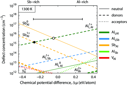
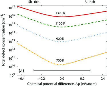
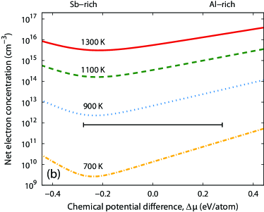
The defect concentrations calculated using the band gap corrected formation energies are shown in Fig. 4 for a representative temperature of 1300 K ( = 1327 K), with the line thicknesses indicating the charge state . Figure 5 shows the dependence of the total defect and net electron concentrations on the chemical environment (chemical potential difference ) for a variety of temperatures. For all cases shown here, the intrinsic (self-consistent) electron chemical potential is located near the middle of the gap, although there are slightly more electrons than holes in the material (intrinsically n-type material).
IV Discussion
An inspection of the -corrected results in the lower panels of Fig. 3 shows that four different defects have the lowest formation energy and are thus the most abundant, depending on the values of the electron chemical potential, , and the chemical potential difference, . The aluminum tetrahedral interstitial is the dominant defect for in the lower half of the band gap (-type material), while the aluminum vacancy is dominant for in the upper half of the band gap (-type material). For Al-rich conditions (left panel in Fig. 3), the AlSb antisite defect can also be important when the material is lightly doped -type (near the crossing with ), particularly considering the uncertainty in the range of vs and the possible errors in the formation energies of up to about 0.1 eV from entropic effects. For Sb-rich conditions (right panel in Fig. 3), the antisite defect (neutral or positively charged) is important over a wide range of , from the -type regime to near the middle of the gap. However, we note that for near the middle of the gap (intrinsic or compensated material), the dominant charged native defect is always , since the relevant defect is uncharged.
In the absence of impurities, the intrinsic electron chemical potential is located near the middle of the band gap (see Sec. III.4). Under this condition, the two relevant defects are therefore the interstitial and the antisite, as illustrated clearly in Fig. 4. By comparison with Fig. 5, we see that the transition point between and that occurs close to corresponds to the minimum in the total defect concentration. In Fig. 5, the dominant defect on the Sb-rich (left) side is , while on the Al-rich (right) side it is . Near the transition (minimum in the curve), the two concentrations are comparable. In contrast, the minimum in the net electron concentration in Fig. 5 is located on the Sb-rich side, corresponding to the crossing of the concentrations of and in Fig. 4. Since the charge neutrality condition [Eq. (6)] depends only on the concentrations of charged defects, the neutral antisites do not contribute to charge compensation or net electron concentration.
As mentioned in Sec. III.4, the calculated electron concentration slightly exceeds the hole concentration for pure material, yielding n-type intrinsic material irrespective of the chemical environment characterized by . This behavior results because the formation energies of acceptor-type defects () always exceed the formation energies of donor-type defects (, ) when the electron chemical potential is close to the middle of the band gap (see Fig. 3). It should be noted that this situation is changed if the material is extrinsically doped. For p-doped material, the donor-type native defects remain dominant and partially compensate the extrinsic dopant. For n-doped material, the ordering of the formation energies is reversed, but the then-dominant acceptor-type native defects still partially compensate the extrinsic dopant.
The temperatures indicated in Figs. 4 and 5 refer to thermal equilibrium conditions at those temperatures. In practice, these temperatures can be interpreted as corresponding to annealing temperatures, with the chemical potential difference referring to the chemical environment of the annealing process (e.g., an Sb overpressure corresponds to Sb-rich conditions; conversely, growth is often performed under Al-rich conditions). The highest temperature considered here, 1300 K, is just below the melting point of 1327 K and might represent melt growth conditions. However, growth is typically performed too rapidly to allow equilibrium to be achieved and the non-equilibrium grown-in defect concentrations will be higher than predicted here. The curves in Fig. 5 essentially represent the predicted concentrations for infinitely long anneals at the specified temperatures.
At 1300 K, the calculated net electron concentration varies roughly between and depending on the chemical potential difference, . If all defects are assumed to be sufficiently mobile down to 700 K so that the material can reach thermal equilibrium at that temperature, then the lowermost curves in Fig. 5 predict a net electron concentration of to and a total defect concentration between and . Since the diffusivity depends exponentially on the inverse temperature, the defect mobilities decrease sharply with temperature. Therefore, as the temperature is further lowered the system will no longer be able to reach the equilibrium concentration in reasonable time, which requires excess defects either to diffuse to the surface or to anneal by recombination. In contrast to lattice defects, the intrinsic electron and hole concentrations, and , readily adjust to temperature changes. The “freezing in” of the defect concentrations is therefore expected to crucially affect the charge neutrality condition upon cooling to low (e.g., room) temperatures (in particular if there are no extrinsic dopants). However, since the diffusivities of the individual defects are currently unknown, we cannot quantitatively describe this “freezing in” of the defect distributions in the present study; thus, predictions of the charge carrier and defect concentrations near room temperature and below may be unreliable. The determination of diffusivities for specific defects, to account for the kinetics of defect “freeze-in,” will be the subject of future work.
Experimentally, AlSb crystals grown from the melt have often been found to display p-type conductivity.KJ_ The present finding that the pure material behaves intrinsically n-type is, however, not in contradiction with this observation. A typical experimental setup employs a graphite susceptor, alumina crucible, and quartz tubes for melting Sb, which are potential sources of various impurities, most importantly carbon, oxygen, silicon, and aluminum.KJ_ In particular, carbon impurities act as acceptors, therefore accidental p-type doping is a very likely scenario which is supported by chemical analysis of grown AlSb crystals and measurements on intentionally doped samples.KJ_ The measured levels of carbon impurities and the experimental observation that the material becomes intrinsic around 1000 K (Ref. [Madelung, 2004]) are consistent with our calculated excess native electron concentration at that temperature. A detailed study of the role of extrinsic defects in AlSb is beyond the scope of the present work; however, the results of ongoing work to elucidate the effects of impurities and to investigate ways to optimize the electronic properties of the material by intentional doping are forthcoming.
V Conclusions
In summary, we have employed density functional theory calculations to study the properties of intrinsic point defects in aluminum antimonide. An exhaustive set of defect configurations —including vacancies, antisites, and interstitials (tetrahedral, hexagonal, and split), with all relevant charge states— was considered based on knowledge of other III-V compounds. Relaxed atomic structures of each defect were carefully determined, and formation energies were calculated to evaluate the equilibrium concentrations of each defect. Strain and electrostatic artifacts related to the use of the supercell approach were carefully removed by employing a finite-size scaling procedure, which involved performing a series of calculations for each defect with supercell sizes ranging from 32 to 216 atoms. The underestimation of the band gap due to the local density approximation was taken into account by applying an a posteriori correction scheme that utilized separate GW calculations to obtain valence and conduction band offsets, which enter the correction.
Aluminum interstitials (), antimony antisites (, ), and aluminum vacancies () were found to be the most dominant defects, depending on the electron chemical potential and the chemical potential difference (chemical environment) of the system. We observe that interstitials and antisites dominate under Al-rich and Sb-rich conditions, respectively. Calculated formation energies were employed in solving the charge neutrality condition to obtain self-consistent defect concentrations and intrinsic electron chemical potential for the pure material at various temperatures. We find the material to be intrinsically weakly n-type and predict both the total defect and the net electron concentrations. Near the melting point, the equilibrium concentration of native defects is predicted to be in the to cm-3 range, while at lower temperatures, it is expected that concentrations down to the cm-3 range or lower can be achieved. The net excess electron density in bulk grown material might be as high as to cm-3 from “freeze-in” of defects from melt solidification.
For extrinsically doped material, which we do not treat explicitly in detail in this work, the dominant native defects depend on the nature of the doping. For n-doped material, and tend to be important, while for p-doped material, and are important, depending on chemical environment (Al-rich vs. Sb-rich). Some amount of self-compensation from the native defects occurs in both cases.
Finally, we note that the present work is part of a concerted research effort which ultimately aims to provide a complete and consistent picture of the point defect properties of AlSb and the relations to carrier transport properties. We are engaged in further theoretical and experimental work to explore the role of extrinsic defects, as well as the scattering behavior of defects on carrier transport. In this context, the present study forms the basis for these future studies, which will be the subjects of forthcoming reports.
Acknowledgements.
This work was performed under the auspices of the U.S. Department of Energy by Lawrence Livermore National Laboratory in part under Contract W-7405-Eng-48 and in part under Contract DE-AC52-07NA27344. The authors acknowledge support from the National Nuclear Security Administration Office of Nonproliferation Research and Development (NA-22) and from the Laboratory Directed Research and Development Program at LLNL. The authors would like to thank Babak Sadigh for fruitful discussions.*
Appendix A Band gap correction of defect formation energies
While DFT calculations typically give very reasonable values for energy differences within a group of bands (e.g., the valence band), energy differences between different groups of bands (i.e., band gaps, e.g., between the valence and conduction bands) are much less reliable. This shortcoming particularly affects the differences between the valence and conduction bands, giving rise to the well-known band gap error.
The incorrect description of the energy differences between different groups of bands can affect the total energy. The most sensitive contribution is the band energy which is given by
| (8) |
where and run over bands and -points, respectively, and and are the occupation numbers and eigenvalues, respectively. Without loss of generality, one can divide the band energy into separate sums over the valence and conduction band states, as
| (9) |
If one assumes rigid levels, which is a reasonable approximation in many cases, the errors in the energy differences between two groups of bands (i.e., across a band gap) can be corrected by adding constant energy shifts to the valence and conduction band states:
| for the valence band, and | |||
The sum of the band shifts, , equals the band gap error. The expression for the corrected band energy then reads
| (10) |
Taking the difference between Eqs. (9) and (10), one obtains the band energy correction term
| (11) |
where is simply the number of unoccupied states in the valence band and is the number of occupied states in the conduction band.
According to Eq. (3), the defect formation energy of charged defects further depends on the position of the valence band maximum. The total correction term for the formation energy thus reads
| (5) |
The energy offsets and can be obtained, for example, from GW calculations, which for many systems provide band gaps and structures in good agreement with experiment.
It is important to realize that this scheme neglects both level relaxations and changes in the double counting term. If these limitations are acceptable, this method offers a simple a posteriori correction of the formation energies. It should furthermore be noted that transition levels are not affected by the relative weight of and . Upon application of this correction scheme, acceptor levels track the valence band maximum while donor transitions follow the conduction band minimum.
References
- Armantrout et al. (1977) G. A. Armantrout, S. P. Swierkowski, J. W. Sherohman, and J. H. Lee, IEEE Trans. Nucl. Sci. N5-24, 121 (1977).
- Owens (2006) A. Owens, J. Synchrotron Rad. 13, 143 (2006).
- Tuttle and Kroemer (1987) G. Tuttle and H. Kroemer, IEEE Trans. Electron Devices ED-34, 2358 (1987).
- Ashley et al. (2007) T. Ashley, L. Buckle, S. Datta, M. T. Emeny, D. G. Hayes, K. P.Hilton, R. Jefferies, T. Martin, T. J. Phillips, D. J. Wallis, et al., Electronic Letters 43 (2007).
- Soderstrom et al. (1991) R. Soderstrom, E. R. Brown, C. D. Parker, L. J. Mahoney, , and T. C. McGill, Appl. Phys. Lett. 58, 275 (1991).
- Canedy et al. (2006) C. L. Canedy, W. W. Bewley, J. R. Lindle, C. S. Kim, M. Kim, I. Vurgaftman, and J. R. Meyer, Appl. Phys. Lett. 88, 161103 (2006).
- Canedy et al. (2007) C. L. Canedy, W. W. Bewley, M. Kim, C. S. Kim, J. A. Nolde, D. C. Larrabee, J. R. Lindle, I. Vurgaftman, and J. R. Meyer, Appl. Phys. Lett. 90, 181120 (2007).
- Devenson et al. (2007) J. Devenson, R. Teissier, O. Cathabard, and A. N. Baranov, Appl. Phys. Lett. 90, 111118 (2007).
- Allnatt and Lidiard (2003) A. R. Allnatt and A. B. Lidiard, Atomic Transport in Solids (Cambridge University Press, Cambridge, 2003).
- Qian et al. (1988) G.-X. Qian, R. M. Martin, and D. J. Chadi, Phys. Rev. B 38, 7649 (1988).
- Zhang and Northrup (1991) S. B. Zhang and J. E. Northrup, Phys. Rev. Lett. 67, 2339 (1991).
- Kresse and Hafner (1993) G. Kresse and J. Hafner, Phys. Rev. B 47, 558 (1993).
- Kresse and Hafner (1994) G. Kresse and J. Hafner, Phys. Rev. B 49, 14251 (1994).
- Kresse and Furthmüller (1996a) G. Kresse and J. Furthmüller, Phys. Rev. B 54, 11169 (1996a).
- Kresse and Furthmüller (1996b) G. Kresse and J. Furthmüller, Comput. Mater. Sci. 6, 15 (1996b).
- Blöchl (1994) P. E. Blöchl, Phys. Rev. B 50, 17953 (1994).
- Kresse and Joubert (1999) G. Kresse and D. Joubert, Phys. Rev. B 59, 1758 (1999).
- Monkhorst and Pack (1976) H. J. Monkhorst and J. D. Pack, Phys. Rev. B 13, 5188 (1976).
- Zhao et al. (2004) Y.-J. Zhao, C. Persson, S. Lany, and A. Zunger, Appl. Phys. Lett. 85, 5860 (2004).
- Erhart et al. (2006) P. Erhart, K. Albe, and A. Klein, Phys. Rev. B 73, 205203 (2006).
- Grecu and Dederichs (1971) D. Grecu and P. H. Dederichs, Phys. Lett. 36A, 135 (1971).
- Dederichs and Pollmann (1972) P. H. Dederichs and J. Pollmann, Z. Physik 255, 315 (1972).
- Makov and Payne (1995) G. Makov and M. C. Payne, Phys. Rev. B 51, 4014 (1995).
- Lento et al. (2002) J. Lento, J.-L. Mozos, and R. M. Nieminen, J. Phys.: Condens. Matter 14, 2637 (2002).
- Erhart and Albe (2007) P. Erhart and K. Albe, J. Appl. Phys. 102, 084111 (2007).
- Persson et al. (2005) C. Persson, Y.-J. Zhao, S. Lany, and A. Zunger, Phys. Rev. B 72, 035211 (2005).
- Hedin (1965) L. Hedin, Phys. Rev. 139A, 796 (1965).
- Gonze et al. (2002) X. Gonze, J.-M. Beuken, R. Caracas, F. Detraux, M. Fuchs, G.-M. Rignanese, L. Sindic, M. Verstraete, G. Zerah, F. Jollet, et al., Comput. Mater. Sci. 25, 478 (2002).
- Goedecker (1997) S. Goedecker, SIAM J. on Scientific Computing 18, 1605 (1997).
- (30) The ABINIT code is a common project of the Université Catholique de Louvain, Corning Incorporated, and other contributors (URL http://www.abinit.org).
- Fuchs and Scheffler (1999) M. Fuchs and M. Scheffler, Comput. Phys. Commun. 119, 67 (1999).
- Troullier and Martins (1991) N. Troullier and J. L. Martins, Phys. Rev. B 43, 1993 (1991).
- Massalski (1986) T. B. Massalski, ed., Binary Alloy Phase Diagrams (ASM International, Metals Park, Ohio, 1986).
- James and Lord (1992) A. M. James and M. P. Lord, Macmillan’s Chemical and Physical Data (Macmillan, London, 1992).
- Madelung (2004) O. Madelung, Semiconductors: Data Handbook (Springer, New York, 2004), 3rd ed.
- Chadi (2003) D. J. Chadi, Mater. Sci. Semicond. Process. 6, 281 (2003).
- Baraff and Schlüter (1985) G. A. Baraff and M. Schlüter, Phys. Rev. Lett. 55, 1327 (1985).
- Chadi (1992) D. J. Chadi, Phys. Rev. B 46, 9400 (1992).
- Laasonen et al. (1992) K. Laasonen, R. M. Nieminen, and M. J. Puska, Phys. Rev. B 45, 4122 (1992).
- Schick et al. (2002) J. T. Schick, C. G. Morgan, and P. Papoulias, Phys. Rev. B 66, 195302 (2002).
- Zollo and Nieminen (2003) G. Zollo and R. M. Nieminen, J. Phys.: Condens. Matter 15, 843 (2003).
- El-Mellouhi and Mousseau (2005) F. El-Mellouhi and N. Mousseau, Phys. Rev. B 71, 125207 (2005).
- Foster et al. (2001) A. S. Foster, V. B. Sulimov, F. L. Gejo, A. L. Shluger, and R. M. Nieminen, Phys. Rev. B 64, 224108 (2001).
- Kohan et al. (2000) A. F. Kohan, G. Ceder, D. Morgan, and C. G. Van de Walle, Phys. Rev. B 61, 15019 (2000).
- (45) K. J. Wu, personal communication.