Integrated Diamond Optics for Single Photon Detection
Abstract
Optical detection of single defect centers in the solid state is a key element of novel quantum technologies. This includes the generation of single photons and quantum information processing. Unfortunately the brightness of such atomic emitters is limited. Therefore we experimentally demonstrate a novel and simple approach that uses off-the-shelf optical elements. The key component is a solid immersion lens made of diamond, the host material for single color centers. We improve the excitation and detection of single emitters by one order of magnitude, as predicted by theory.
Over the last decade, solid-state optically-active defects have attracted attention owing to applications in quantum information science. Among numerous studied color centers in diamond, the negatively-charged nitrogen-vacancy (NV) defect is particularly interesting. For the NV-center a variety of applications has been demonstrated, such as diamond-based single photon sources Kurtsiefer et al. (2000); Beveratos et al. (2001), spin based magnetic field sensors Balasubramanian et al. (2008); Maze et al. (2008) and diamond-based quantum information protocols Weber et al. (2010). Its spin state can be coherently manipulated with high fidelity Fuchs et al. (2009) owing to long coherence time Balasubramanian et al. (2009). Moreover, the spin of NV defects can be efficiently read out Neumann et al. (2010) and coupled to photons through spin-dependent transitions Togan et al. (2010), a key ingredient towards long-distance quantum communications using photons as flying qubits.
For all above mentioned experiments the photon collection efficiency is crucial. For single NV defects this is reduced by the high refractive index of diamond (), owing to total internal reflection at the diamond-air interface. Therefore several approaches to increase the collection efficiency, such as optical elements like metallic nanoantenna Schietinger et al. (2009) or photonic wire microcavities Babinec et al. (2010), have been suggested. Improving light extraction from diamond can also be achieved by using NV defects hosted in nanocrystals with a size smaller than the emission wavelength. In this case, refraction becomes irrelevant and the defect can be considered as a point source emitting in the surrounding medium. However, the spin properties of nanocrystals are often affected by surface defects leading to a short coherence time. To overcome these limitations we engineer a solid immersion lens directly into the host material diamond Mansfield and Kino (1990); Hadden et al. (2010).
To estimate theoretically the collection efficiency, we assume a single emitter in diamond and use geometrical optics and Fresnel’s reflection laws. For a single emitting dipole the normalized photoluminescence (PL) intensity (resp. ) having (resp. ) polarization can be calculated as Zwiller and Björk (2002)
| (1) | |||||
| (2) |
where is the emission angle and the azimuthal angle measured from the dipole axis.
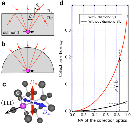
We first consider a dipole beneath a planar diamond surface (Fig. 1(a)). For the moment we assume the dipole is oriented parallel to the surface. The more general case will be treated below. At the diamond interface, Snell’s law imposes , where is the propagation angle in the collection optics medium, characterized by a refractive index . As a result, most of the PL is trapped inside the diamond matrix, since total internal reflection is achieved as soon as . For a diamond-air interface this limits the collection angle to . The effective numerical aperture (NA) over which the dipole radiation will be integrated reads .
The collection efficiencies and are obtained by integrating over the solid angle defined by the NA of the collection optics, leading to
| (3) |
where and are respectively the transmission coefficients of the and polarization components through the interface.
We now consider a dipole located at the center of a hemispherical diamond SIL used as primary collection optic (Fig. 1(b)). In that case, all light rays exit the SIL in a direction normal to the surface, thus avoiding any refraction at the interface. Note that thereby also all chromatic abberations are suppressed. As a result, the collection efficiencies and are defined by equation (3), while using and .
In the general case the collection efficiency depends on the dipole orientation inside the diamond matrix. For NV defects, the PL is associated with two orthogonal dipoles and located in a plane perpendicular to the NV defect symmetry axis Epstein et al. (2005), which is a crystalline axis (Fig. 1(c)). In addition, the absolute orientation of the two transition dipoles is determined by the direction of non-axial local strain in the diamond matrix. Since local strain is randomly distributed over a diamond sample, the orientation of the two orthogonal dipoles is random in a plane perpendicular to the NV defect symmetry axis.
For a -oriented diamond sample, the absolute angle between the NV defect axis and the diamond flat surface is the same for the four possible NV defect orientations 111The NV defect can be oriented along [], [], [], or [] direction.. To evaluate the collection efficiencies for this case, we take into account the orientation of the two dipoles with respect to the flat diamond surface and apply the required rotations to equation (3). An average over the two dipoles and over all possible strain-induced orientations is taken. The results of the calculation are shown on Fig. 1(d). Using a -NA microscope objective, the collection efficiency is for a planar diamond surface and reaches with a hemispherical diamond SIL. From this geometrical considerations, a 7.5-fold enhancement in collection efficiency is therefore expected for that particular NA of the collection optics. Note that this theoretical value requires a diamond SIL with a surface roughness of approximatively Baba et al. (1999).
A diamond SIL was fabricated as follows. Homoepitaxial chemical vapor deposition (CVD) diamond growth was performed using a selected high pressure high temperature grown substrate, which had been carefully processed prior to growth in order to minimize the dislocation density in the grown CVD diamond. A two stage chemical process was subsequently used to produce a grown CVD layer with a thickness of about 2.3 mm made up with a first layer containing 0.2 ppm of single substitutional nitrogen. The final layer of 0.6 mm was engineered with a significant reduced nitrogen concentration ( ppb), to reduce the number of native NV defects. The SIL was subsequently processed from this CVD diamond sample, the flat surface being composed by the high purity layer described above, oriented along a crystalline axis. Using a combination of laser and mechanical processing stages 222Nelissen, W. et al., Patent WO 2007/007126A1, international publication date 18/01/2007., a 1-mm diameter SIL was produced with flatness better than 10 nm (rms), measured by atomic force microscopy.
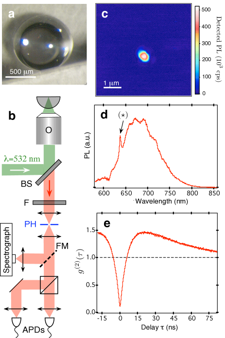
Native single NV defects in the diamond SIL were imaged using conventional confocal microscopy, as depicted in figure 2(b). A frequency doubled Nd:YAG laser ( nm) was tightly focused onto the flat surface of the diamond SIL using a -NA microscope objective. The PL was collected by the same objective using the SIL as primary collection optics, and spectrally filtered from the remaining excitation light. The collected light was then focused onto a m diameter pinhole and directed either to a spectrometer or to a Hanbury-Brown and Twiss (HBT) interferometer for photon correlation measurements. A PL raster scan of a region close to the center of the diamond SIL is depicted in figure 1(b), showing an isolated photoluminescent spot. The spectrum recorded at this point exhibits a broadband emission with a characteristic zero-phonon line at the wavelength nm (Fig 2(d)) which is associated with an NV defect. We note that optical aberrations can be clearly observed in the confocal raster scan, since the shape of the bright spot is not perfectly circular. Such aberrations are attributed to a lateral offset of m between the NV defect location and the center of the diamond SIL Baba et al. (1999).
To proof that research was performed on a single emitter, we measured the time delay histogram between two consecutive single-photon detections using a standard HBT interferometer. After normalization to a Poissonnian statistics, the recorded histogram is equivalent to a measurement of the second-order autocorrelation function defined by
| (4) |
where is the PL intensity at time . As shown in Fig. 2(e), a sub-poissonian photon statistics () is observed, proving a single NV defect.
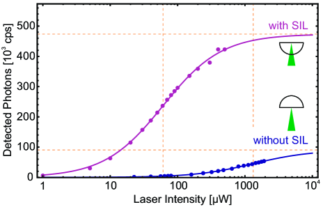
With the aim of quantifying the enhancement in collection efficiency, the PL rate was measured as a function of the laser intensity (Fig. 3). Experimental data were then fitted using a two-level model with the relation
| (5) |
where is the saturation laser intensity for the given focus size and the emission rate at saturation. For the studied single NV defect imaged through the diamond SIL, we find cps and W. At this saturation intensity the photon emission is enhanced by two orders of magnitude with respect to a collection in a bulk diamond. This we check by a single NV defect imaged from the backside of the SIL, i.e. imaged through a planar diamond surface. In that configuration, the saturation parameters are cps and W. A more than 6-fold enhancement is therefore achieved in high saturation conditions. Such a value is slightly smaller than the one predicted by pure geometrical optic arguments (Fig. 1(d)). This discrepancy is attributed to optical aberrations arising from unperfect positioning of the NV defect in the center of the diamond SIL Baba et al. (1999). We note that similar collection efficiency enhancements were obtained for two others single NV defects located around m away from the center of the SIL. However, if this distance exceeds m, the enhancement vanishes. A precise positioning of NV defects at the center of the SIL can be achieved by controlled ion implantation Meijer et al. (2005). In addition, collection efficiency could be further improved by using an anti-reflection coating on the hemispheric surface and/or a properly designed Bragg mirror deposited on the SIL flat surface, in order to collect backwards emitted photons.
Beyond collection efficiency enhancement, we note that exciting through the diamond SIL yields to a smaller excitation volume. Indeed, the saturation laser intensity is decreased by roughly one order of magnitude while exciting a single NV defect through the diamond SIL. This effect might have interesting applications in the context of stimulated emission depletion (STED) microscopy, since the resolving power of STED is proportional to Rittweger et al. (2009). Furthermore, the reduced focus of the excitation laser funnels more efficiently photons towards the single emitter. This allows for the detection of a single defect in transmission through an efficient extinction of the excitation laser beam Wrigge et al. (2008).
Acknowledgements
This work was supported by the EU, DFG, Landesstiftung BW, BMBF, Volkswagen Stiftung and NIH.
Additional Information
Patent application related to data present in this manuscript is under submission process. Correspondence and requests for materials should be addressed to V.J. (vincent.jacques@lpqm.ens-cachan.fr) and F.J. (f.jelezko@physik.uni-stuttgart.de).
References
- Kurtsiefer et al. (2000) C. Kurtsiefer, S. Mayer, P. Zarda, and H. Weinfurter, Phys. Rev. Lett. 85, 290 (2000), URL http://link.aps.org/doi/10.1103/PhysRevLett.85.290.
- Beveratos et al. (2001) A. Beveratos, R. Brouri, T. Gacoin, J.-P. Poizat, and P. Grangier, Phys. Rev. A 64, 061802 (2001), URL http://link.aps.org/doi/10.1103/PhysRevA.64.061802.
- Balasubramanian et al. (2008) G. Balasubramanian, I. Y. Chan, R. Kolesov, M. Al-Hmoud, J. Tisler, C. Shin, C. Kim, A. Wojcik, P. R. Hemmer, A. Krueger, et al., Nature 455, 648 (2008), URL http://dx.doi.org/10.1038/nature07278.
- Maze et al. (2008) J. R. Maze, P. L. Stanwix, J. S. Hodges, S. Hong, J. M. Taylor, P. Cappellaro, L. Jiang, M. V. G. Dutt, E. Togan, A. S. Zibrov, et al., Nature 455, 644 (2008), URL http://dx.doi.org/10.1038/nature07279.
- Weber et al. (2010) J. R. Weber, W. F. Koehl, J. B. Varley, A. Janotti, B. B. Buckley, C. G. Van de Walle, and D. D. Awschalom, Proceedings of the National Academy of Sciences 107, 8513 (2010), URL http://www.pnas.org/content/107/19/8513.abstract.
- Fuchs et al. (2009) G. D. Fuchs, V. V. Dobrovitski, D. M. Toyli, F. J. Heremans, and D. D. Awschalom, Science 326, 1520 (2009), URL http://www.sciencemag.org/cgi/content/abstract/326/5959/1520.
- Balasubramanian et al. (2009) G. Balasubramanian, P. Neumann, D. Twitchen, M. Markham, R. Kolesov, N. Mizuochi, J. Isoya, J. Achard, J. Beck, J. Tissler, et al., Nature Materials 8, 383 (2009), URL http://dx.doi.org/10.1038/nmat2420.
- Neumann et al. (2010) P. Neumann, J. Beck, M. Steiner, F. Rempp, H. Fedder, P. R. Hemmer, J. Wrachtrup, and F. Jelezko, Science 329, 542 (2010), URL http://www.sciencemag.org/cgi/content/abstract/329/5991/542.
- Togan et al. (2010) E. Togan, Y. Chu, A. S. Trifonov, L. Jiang, J. Maze, L. Childress, M. V. G. Dutt, A. S. Sorensen, P. R. Hemmer, A. S. Zibrov, et al., Nature 466, 730 (2010), URL http://dx.doi.org/10.1038/nature09256.
- Schietinger et al. (2009) S. Schietinger, M. Barth, T. Aichele, and O. Benson, Nano Letters 9, 1694 (2009), URL http://pubs.acs.org/doi/abs/10.1021/nl900384c.
- Babinec et al. (2010) T. M. Babinec, B. J. M. Hausmann, M. Khan, Y. Zhang, J. R. Maze, P. R. Hemmer, and M. Loncar, Nature Nanotechnology 5, 195 (2010), URL http://dx.doi.org/10.1038/nnano.2010.6.
- Mansfield and Kino (1990) S. M. Mansfield and G. S. Kino, Applied Physics Letters 57, 2615 (1990), URL http://link.aip.org/link/?APL/57/2615/1.
- Hadden et al. (2010) J. P. Hadden, J. P. Harrison, A. C. Stanley-Clarke, L. Marseglia, Y-L. D. Ho, B. R. Patton, J. L. O’Brien, and J. G. Rarity, ArXiv e-prints (2010), eprint 1006.2093, URL http://arxiv.org/abs/1006.2093.
- Zwiller and Björk (2002) V. Zwiller and G. Björk, Journal of Applied Physics 92, 660 (2002), URL http://link.aip.org/link/?JAP/92/660/1.
- Epstein et al. (2005) R. J. Epstein, F. M. Mendoza, Y. K. Kato, and D. D. Awschalom, Nature Physics 1, 94 (2005), URL http://dx.doi.org/10.1038/nphys141.
- Baba et al. (1999) M. Baba, T. Sasaki, M. Yoshita, and H. Akiyama, Journal of Applied Physics 85, 6923 (1999), URL http://link.aip.org/link/?JAP/85/6923/1.
- Meijer et al. (2005) J. Meijer, B. Burchard, M. Domhan, C. Wittmann, T. Gaebel, I. Popa, F. Jelezko, and J. Wrachtrup, Applied Physics Letters 87, 261909 (pages 3) (2005), URL http://link.aip.org/link/?APL/87/261909/1.
- Rittweger et al. (2009) E. Rittweger, K. Y. Han, S. E. Irvine, C. Eggeling, and S. W. Hell, Nature Photonics 3, 144 (2009), URL http://dx.doi.org/10.1038/nphoton.2009.2.
- Wrigge et al. (2008) G. Wrigge, I. Gerhardt, J. Hwang, G. Zumofen, and V. Sandoghdar, Nature Physics 4, 60 (2008), URL http://dx.doi.org/10.1038/nphys812.