Single valley Dirac fermions in zero-gap HgTe quantum wells
Abstract
Dirac fermions have been studied intensively in condensed matter physics in recent years. Many theoretical predictions critically depend on the number of valleys where the Dirac fermions are realized. In this work, we report the discovery of a two dimensional system with a single valley Dirac cone. We study the transport properties of HgTe quantum wells grown at the critical thickness separating between the topologically trivial and the quantum spin Hall phases. At high magnetic fields, the quantized Hall plateaus demonstrate the presence of a single valley Dirac point in this system. In addition, we clearly observe the linear dispersion of the zero mode spin levels. Also the conductivity at the Dirac point and its temperature dependence can be understood from single valley Dirac fermion physics.
I Introduction
In recent years, Dirac fermions have been intensively studied in a number of condensed matter systems. In the two dimensional material graphene the low energy spectrum is well described by two spin degenerate massless Dirac cones at two inequivalent valleys, giving rise to four massless Dirac cones in totalsemenoff1984 ; divincenzo1984 . The fabrication of graphene sheets enabled substantial experimental progress in this field, and the physics of the Dirac fermions has been investigated extensivelycastro2009 . At the same time, many theoretical predictions rely on a single Dirac cone valley, or, at least, weak inter-valley scatteringcastro2009 . Graphene is not a suitable platform to test these latter predictions because of the presence of two valleys and strong inter-valley scattering. In addition, it is presently unclear how an energy gap can be reliably generated in single layer graphene, which would be desirable for a variety of device applications.
A HgTe/CdTe quantum well is another system where Dirac fermion physics emergesbernevig2006d ; koenig2007 . In this case, the Dirac fermions appear only at a single valley, at the point of the Brillouin zone. Furthermore, tuning the thickness of the HgTe quantum well continuously changes both the magnitude and the sign of the Dirac mass. When is less than a critical thickness nm, the system is in a topologically trivial phase with a full energy gap. On the other hand, when , the quantum spin Hall state is realized, where a full energy gap in the bulk occurs together with gapless spin-polarized states at the edge. The experimental discovery of this statekoenig2007 provides the first example of a time-reversal invariant topological insulator in naturekoenig2008 . A topological quantum phase transition is predicted to occur when , where a massless Dirac fermion state is realized at a single valley, with both spin orientationsbernevig2006d . Our paper reports the experimental discovery of such a state.
In a two dimensional system with time reversal symmetry and half integral spin, a minimal number of two massless Dirac cones can be present, as can be proven by a simple generalization of a similar theorem in one dimensionwu2006 . General results of this type have first been discovered in lattice gauge theory, and are known as chiral fermion doubling theoremsnielsen1981 . In this sense, the HgTe quantum well at the critical thickness realizes this minimal number of two Dirac cones in two dimensionsfootnote .
II HgTe quantum wells as half-graphene
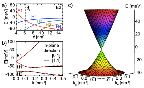
HgTe is a zinc-blende-type semiconductor with an inverted band structure. Unlike conventional zinc-blende semiconductors, and due to the very strong spin-orbit coupling in the material, the band of HgTe (which derives from chalcogenide p-orbitals), has a higher energy than the band that originates from metallic s-orbitals and usually acts as the conduction band. Consequently, in HgTe/(Hg,Cd)Te quantum wells, when the well thickness is large enough, the sub-bands of the quantum well are also inverted: derived heavy hole-like (H) sub-bands have higher energies than -based electron-like (E) sub-bands. The inverted band structure, especially the inversion between and sub-bands (where the suffix is the sub-band number index), leads to the occurrence of the quantum spin Hall effectbernevig2006d ; koenig2007 , boasting dissipationless edge channel transport at zero external magnetic fieldroth2009 . When the thickness of the quantum well is decreased, the energies of the sub-bands increase due to quantum confinement, while those of the sub-bands decrease, as shown in Fig 1 (a). Eventually, the sub-band gains a higher energy than the sub-band and the system has the normal band sequence. The different dependence of and sub-bands on well thickness implies that there must exist a critical thickness where the band gap is closed. In fact, the crossing point between and sub-bands, denoted as in Fig 1 (a), not only corresponds to the critical point for the quantum phase transition between quantum spin Hall insulator and normal insulatorbernevig2006d but additionally yields a quantum well whose low-energy band structure closely mimics a massless Dirac Hamiltonian.
When nm, the energy dispersion of the and sub-bands, which can be calculated from an 8-band Kane model, is found to linearly depend on the momentum near the point of the Brillouin zone, as shown in Fig 1 (b) and (c). Near the point, using the states , , and as a basis, one can write an effective Hamiltonian for the and sub-bands, as followsbernevig2006d
| (3) | |||
| (4) |
where
| (5) |
The two components of the Pauli matrices denote the and sub-bands, while the two diagonal blocks and of represent spin-up and spin-down states, related to each other by time reversal symmetry. At the critical thickness, the relativistic mass in (5) equals to zero. If we then only keep the terms up to linear order in for each spin, or correspond to massless Dirac Hamiltonians. A HgTe quantum well at is thus a direct solid state realization of a massless Dirac Hamiltonian. Since it does not have any valley degeneracy, a HgTe/(Hg,Cd)Te quantum well is, in a sense, half-graphene. Besides the linear term forming the Dirac Hamiltonian, there are additional effects in the HgTe Dirac system, such as the quadratic terms in (4), and the presence of Zeeman- and inversion asymmetry-induced terms, which are discussed in detail in the supplementary material.
As explained in the introduction, a two-cone Dirac system is the simplest possible realization of Dirac fermions for any two dimensional quantum well or thin film, which makes HgTe a very interesting model system to investigate Dirac fermion physics. Other benefits include the very high mobility (up to cm2/Vs for high carrier densities) and the possibility to study the effects of a finite relativistic mass (with both positive and negative sign). In this paper, we describe magneto transport experiments on gated zero gap HgTe wells that clearly demonstrate the Dirac fermion physics expected from Eqs. (4) and (5).
III Experimental
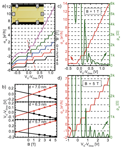
For these studies, we have grown by molecular beam epitaxy a number of modulation-doped HgTe/Te quantum well structures on lattice-matched (Cd,Zn)Te substrates, with a nominal well width ranging from 5.0 to 7.5 nm (yielding various relativistic masses ), including several samples aiming for the critical thickness of 6.3 nm. From Fig. 1 (a), the reader can infer that the series includes both normal and inverted band gap structures. From X-ray reflectivity measurements on our quantum well structuresstahl2010 we infer the existence of thickness fluctuations of the order of a monolayer in the samples, which corresponds to fluctuations in of around 1 meV. Subsequently, the wafers have been processed into Hall bar devices with dimensions (length width ) of (600 200) and (20.0 13.3) m2 using a low temperature positive optical lithography process. For gating purposes a 100 nm thick multilayer gate insulator and a 5/50 nm Ti/Au gate electrode are deposited. Ohmic contacts are made by thermal indium bonding. A micrograph of such a Hall bar device is shown in the inset of Fig.2 (a). At zero gate voltage, the devices are n-type conducting with carrier concentrations around and mobilities of several .
Transport measurements are carried out in a variable temperature magneto-cryostat at a temperature of 4.2 K, unless indicated otherwise. Typically, a bias voltage of up to 10 mV is applied between current contacts 1 and 6 (as denoted in the inset of Fig. 2(a) ), resulting in a current I of approximately 1 A , as determined by measuring the voltage drop across a reference resistor in series with the sample. The resulting longitudinal (, contacts 3 and 5) and transverse (, contacts 2 and 3) voltages are detected simultaneously yielding the longitudinal () and transverse () resistivities.
Applying a gate voltage between the top gate and the 2DEG, the electron density (and thus the Fermi energy) can be adjusted. As reported previously, the carrier type can be varied from n-type conductance for positive to p-type behavior for negative . Hysteresis effects due to interfacial states hinz2006 restrict the usable range of gate voltages to V. For reasons of comparison, we have adjusted the gate voltage axes in Figs. 2, 3 and 4 such that V corresponds to the Dirac point. varies from cool-down to cool-down, but typically is of order -1.2 V.
IV Quantum Hall effect and the identification of zero-gap samples
In Fig. 2(a) we plot the Hall conductivity at various fixed magnetic fields for a sample with nm as a function of the gate voltage. The conductivity axis is correct for the trace taken at 1 T, while the traces for higher fields have been offset by a constant amount (in this case one conductance quantum) per Tesla, for reasons that will become obvious shortly. First, we note that the traces show well developed quantum Hall plateaus, even for fields as low as 1 T. At this low field, the spin-derived Hall-plateaus (the conductance plateaus at an even integer times ) are still less broad than the orbital-induced ones (plateaus at an odd integer times ), which facilitates their assignment. Obviously, because of the large g-factor of HgTe ( for this well, see below) the Landau levels are always spin-resolved. A full assessment of Dirac behavior will thus have to come from the field and energy dependence of the Landau level structure, which we will provide below.
First, we will address another question - is the sample really zero gap? Since MBE growth calibration is not sufficiently precise to consistently grow a quantum well of exact critical thickness, we require another independent means to assess the well thickness. We have found a simple procedure by analyzing the quantum Hall data of our samples. Specifically, it turns out that the crossing point of the lowest Landau levels for the electron and heavy-hole sub-bands is a precise measure of well thickness. By solving the Landau levels of the effective Hamiltonian (4) in a magnetic field, we find that each of the spin blocks exhibits a ’zero mode’ (n=0 Landau level), which is one of the important differences between Landau levels of materials described by a Dirac Hamiltonian and those of more traditional metalsjackiw1984 . The energy of the zero mode is given by
| (6) |
for the spin-up and spin-down block, respectively. Here is the perpendicular magnetic field. The spin splitting, given by , thus increases linearly with magnetic field. From (6), we find that there is a critical magnetic field , where the two zero mode spin levels become degenerate, . In the inverted regime , this degeneracy occurs at a positive magnetic field , while in the normal regime where , the crossing extrapolates to a negative value of . For a well exactly at the critical thickness we have , and the crossing point will occur at zero field, . Therefore the position of the crossing point of the spin states of the lowest electron and hole Landau levels at zero magnetic field will give us a direct indication for the existence of a Dirac point () in the quantum well.
Applying this procedure to the experimental data of Fig. 2 (a) (and similar data from the other quantum wells in our growth series) is straightforward. Since the Landau levels are already well defined at small magnetic fields, we can easily identify the Landau levels corresponding to the two spin blocks of the zero mode as the boundaries of the plateau, at various magnetic fields. The constant offset between the different plots in Fig. 2 (a) implies that we can now translate the vertical axis into a field axis with a spacing of 1 T between the scans (the ”B”-axis in the figure) and we can directly plot the linear spin splitting predicted by Eq. (6) in Fig. 2 (b). Extrapolating the linear behavior in the graph allows us to determine , which in this case leads to T - this sample has a Dirac mass close to zero.
As an illustration of the efficiency and sensitivity of this procedure, Fig. 2 (b) shows the extraction of for three different samples. The sample in the upper panel has an inverted band structure since (from a more detailed fit we find nm). The middle panel corresponds to the data of Fig. 2 (a), where the intersection is at , corresponding to , and finally the sample in the bottom panel has a not-inverted band structure since the crossing point occurs for (and corresponds to a well-width of approximately 5.7 nm).
V Further characterization of a zero-gap sample
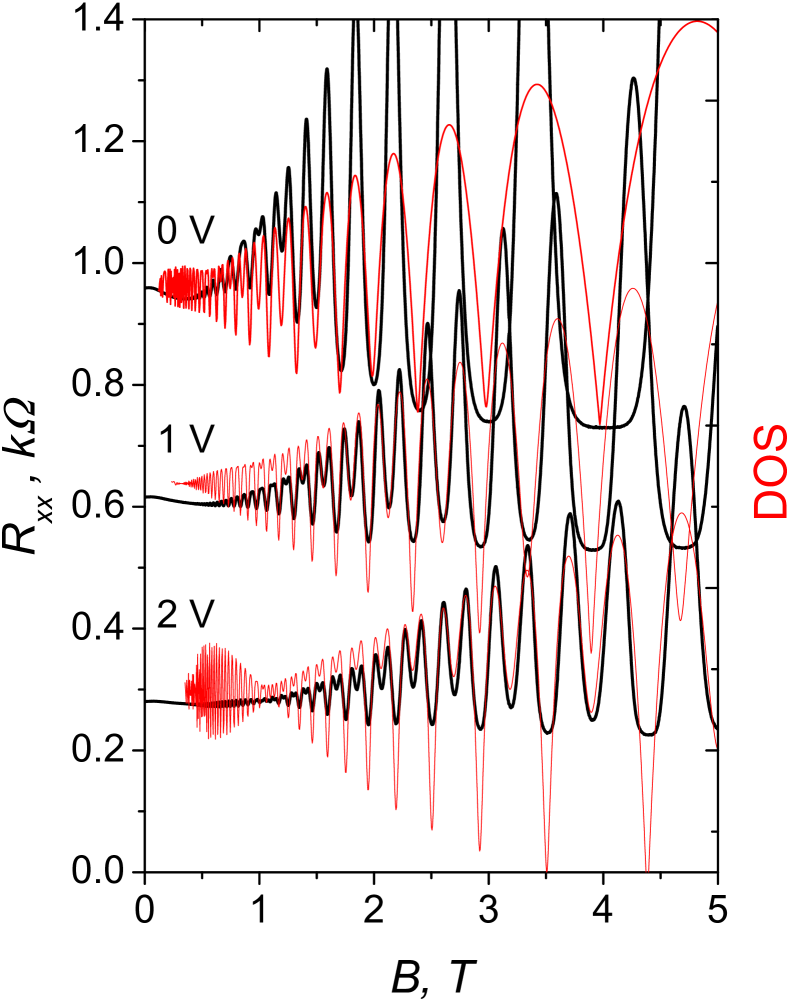
In the following, the sample with T of Fig.2 (b) is further investigated. Figs. 2 (c) and (d) show the Hall conductivity of this sample at 1 and 5 T, respectively, in combination with the Shubnikov-de Haas oscillations in the longitudinal resistance. The first thing to note is the quantization of the Hall plateaus. Orbital quantization yields plateaus at odd multiples of , with additional even-integer plateaus due to spin splitting already observable at 1 T. This is the unusual ordering of the Hall plateaus that results from the Dirac Hamiltoniancastro2009 . Moreover, the observed plateaus occur at one half the conductance of the plateaus observed for graphenenovoselov2005 ; zhang2005 - a direct consequence of the fact that the HgTe quantum well only has a single (spin degenerate) Dirac cone, where graphene has two. Furthermore, we always observe a plateau at zero conductance in the Hall traces, which is different from the low-field behavior in graphenecastro2009 . The zero conductance Hall plateau is always accompanied by a quite large longitudinal resistivity, which is once more an indication that - already at 1T - the sample is gapped due to spin splitting.
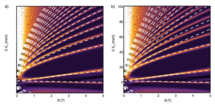
To further validate our claim that this sample boasts a zero gap Dirac Hamiltonian at low energies, we plot in Fig.3 (a) a Landau level fan chart. This chart was obtained by plotting the derivative in a color-coded 3-dimensional graph as a function of both and . When the sample exhibits a quantum Hall plateau, the Hall conductance obviously is constant and its derivative is zero; when a Landau level crosses the Fermi energy, reaches a maximum, which can be conveniently indicated by the color coding. To translate the gate voltage axis to an energy scale for the band structure, we assume that the gate acts as a plane capacitor plate, and calculate the electron density in the quantum well as a function of energy using our 8-band modelnovik2005 , assuming the well has the critical thickness nm. Furthermore, in the supplementary material, we calculate the density of states as a function of magnetic field for fixed electron density and compare the results with the experimental data on the Shubnikov-de Haas oscillations. The good agreement of the node position and spin splitting between the experiment and theory verifies the validity of the 8-band model. The dashed white lines in Fig.3 (a) give the Landau level dispersion predicted by our calculation; the very good agreement with the experimental peaks in is evidence that our to conversion is self-consistent.
The Landau-level dispersion in Fig. 3 (a) shows all the characteristics expected from our Dirac Hamiltonian (4). Besides the zero mode of Eq.(6), solving the Landau levels of the effective Hamiltonian (4) in a magnetic field, yields for the higher Landau levels () ():
| (7) |
where , refer to the two spin blocks of our Dirac Hamiltonian, Eq. (4), and denote the conduction and valence band, respectively. With optimized parameters ( we use meV, meVnm2, meVnm2, meVnm ) the Landau level dispersion described by Eq. (7) are plotted (dashed white lines) as a function of magnetic field in Fig. 3 (b). Clearly, the Dirac model agrees well with our experiment for low magnetic field and low-index Landau levels, but gradually breaks down when the magnetic field is increased.
In the low magnetic field limit, one easily finds that Eq. (7) (for the conduction band) reduces to up to linear terms. This corresponds to the square-root magnetic field dependence that has meanwhile become the signature of Dirac fermion behavior in graphenecastro2009 , with an additional linear term reflecting the large effective g-factor of the HgTe quantum well. Defining , we find . There are two physical origins for the large . Due to the zero gap nature of the present system, the most important contribution comes from orbital effects which are fully incorporated in the Dirac Hamiltonian. However, there is also a contribution from Zeeman-type terms, which is not included in the Dirac Hamiltonian (4). This term is less important than the orbital part and will be discussed in the supplementary material.
Another effect that is not included in our model Dirac Hamiltonian is the inversion asymmetry of the system. In principle, the HgTe quantum well has structural (SIA) and bulk inversion asymmetry (BIA) koenig2008 ; rothe2010 , both of which can couple Dirac cones with opposite spin. From the node position of Shubnikov-de Haas oscillations (the data are presented in the supplementary material), we find that the spin splitting due to SIA is less than 2.5 meV at the largest experimentally accessible Fermi energy, decaying rapidly with densityrothe2010 . The present experiment does not show any evidence of the BIA term; a previous theoretical estimate shows that the BIA term has an energy scale of about 1.6 meVkoenig2008 . We conclude that also the SIA and BIA terms are small compared to the other terms in the Dirac Hamiltonian of Eq. (4). Moreover, they cannot cause the opening of a gap in the quantum well spectrum. The relevance of SIA and BIA terms is discussed in more detail in the supplementary material.
VI Zero field behavior
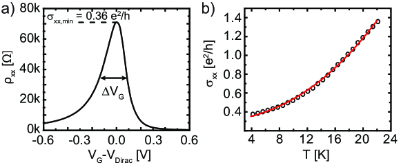
Having thus established that we indeed can describe our quantum well as a zero gap Dirac system, we now turn to its characteristics at zero magnetic field. Fig. 4 (a) plots the resistivity vs. gate voltage, often called the Dirac-peak in the graphene community, in this limit. The graph clearly shows the expected peaked resistivity and exhibits an asymmetry between n- and p-regime which can be attributed to the large hole mass (increased density of states). In graphene, the width of the Dirac-peak is often regarded as a measure of the quality of the sample bolotin2008 . The width of the Dirac peak in Fig. 4 (a) corresponds to a carrier depletion of about cm-2, which is comparable with the situation found in suspended graphene.
At the Dirac point, we find a minimum conductivity of at 4.2 K. Its temperature dependence is shown in Fig. 4 (b), which conveys an initially quadratic temperature dependence, that for temperatures above about 12 K turns linear. The existence of a finite minimal conductivity at vanishing carrier density is a topological (Berry phase) manifestation of the conical singularity of the Dirac bands at . Therefore, our observation of a minimal conductivity in HgTe quantum wells provides independent evidence for the Dirac fermion behavior in this material. The observed minimal conductivity (close to Fradkin86b ; twor2006 ) and the crossover from quadratic () to linear () increase with temperature can be understood from calculations based on the Kubo formula, in which the current-current correlation function is evaluated for the effective Dirac Hamiltonian of Eq. (4), assuming the presence of both well width fluctuations and potential disorder and including only the dominant terms linear in . The details of these calculations are described in the supplementary material. Qualitatively, the temperature dependence of is
| (8) | |||
| (9) |
where is the spectral broadening induced by spin-independent potential disorder. In Eq. (8) the factor of 2 accounts for the spin degeneracy and is the variance of the gap due to spatial deviations of the thickness from the critical value . From the X-ray reflectvity data on our samplesstahl2010 , we estimate meV. This is comparable with typical values of estimated from the self-consistent Born approximation (see supplementary material). Therefore, for the zero-temperature conductivity is approximately , in agreement with the data. The correction reflects the spectral smearing at energies below . In contrast, at the linear T-dependence of (9) reflects the linear density of states, which is another manifestation of the Dirac fermion physics in HgTe quantum wells.
In conclusion, our paper reports the first experimental discovery of a two dimensional massless Dirac fermion in a single valley system. The high mobility in the HgTe quantum wells should allow us to directly study ballistic transport phenomena that so far have been hard to access for Dirac fermionsdu2008 . Moreover, the material offers an additional parameter for the experiments in that the effects of a finite Dirac mass can now be studied in detail.
Acknowledgements. We acknowledge useful discussions with C. Gould and X.L. Qi and thank E. Rupp and F. Gerhard for assistance in sample growth and in the transport experiments. This work was supported by the German Research Foundation DFG (SPP 1285 ’Halbleiter Spintronik’, DFG-JST joint research program, Emmy Noether program (P.R.) and grants AS327/2-1 (E.G.N.), the Alexander von Humboldt Foundation (C.X.L. and S.C.Z.) and the US Department of Energy, Office of Basic Energy Sciences, Division of Materials Sciences and Engineering, under contract DE-AC02-76SF00515 (S.C.Z).
VII Supplementary online material
In the supplementary material , we will give theoretical details connected with the analysis of the effective factor, Shubnikov de Haas oscillations and minimum conductivity in HgTe quantum wells.
VII.1 Effective Hamiltonian for HgTe quantum wells
In this section, we will discuss the complete expression of the effective Hamiltonian of HgTe quantum wells near the critical thickness . As first described by Bernevig, Hughes and Zhangbernevig2006d , the low energy physics of HgTe quantum wells is determined by four states , , and . With these four states as basis, the complete Hamiltonian of the system when a magnetic field is applied in the the z-direction can be written as
| (10) |
The effective Hamiltonian is given by Eq. (1) in the main part of the article, where a Peierls substitution has been applied ( is the magnetic vector potential). All parameters , , , and can be determined by fitting to the experimental Landau level dispersion at K for (we neglect in our calculations the dependence of the parameters on the electron density), which are listed in the table 1.
The Zeeman term has the formkoenig2008
| (15) |
with and the four band effective g-factor () for () bands.
Since in HgTe quantum wells the inversion symmetry is broken, we also need to discuss two terms that result from inversion asymmetry, i.e. the structural inversion asymmetry (SIA) term and the bulk inversion asymmetry (BIA) term. The SIA term is due to the asymmetry of the quantum well potential and has the formrothe2010
| (20) |
In (001) grown HgTe quantum wells,, the Rashba spin splitting is dominantly responsible for the beating pattern of the Shubnikov-de Haas oscillations. By comparing the results of a Kane model calculation with the experimental data, one can thus directly determine the Rashba coefficient. As discussed in the following section, we find that for a quite large range of gate voltages, the Rashba spin splitting is less than 2.5 meV near the Fermi energy, which corresponds to meVnm, meVnm2 and meVnm3. Furthermore we find that the electron Rashba splitting is always dominant over the other two terms.
Since the zinc-blend crystal structure of HgTe is not inversion-symmetric, additional BIA terms appear in the effective Hamiltonian, given bykoenig2008
| (25) |
Since the BIA Hamiltonian is a constant term, it will only change the the Dirac point to a circle and the system remains gapless. An early estimate of magnitude of BIA term gives meVkoenig2008 , which is of the same order of magnitude as the disorder broadening and the fluctuations of the band gap due to variations in well width. Therefore in the present experiment we do not find evidence of a pronounced effect from this term.
| 373 | |
|---|---|
| -857 | |
| -682 | |
| -0.035 | |
| 1.6 | |
| 18.5 | |
| 2.4 |
Neglecting the SIA and BIA terms, the Landau level spectrum is described by
| (26) |
where , and () for the conduction (valence band) and the parameter is taken to be zero, setting the Dirac point at zero energy. The zero mode states () have the dispersion:
| (27) |
and the zero mode splitting is:
| (28) |
Finally, we note that the total spin splitting, defined as the energy difference between the spin-up and spin-down zero modes, has two origins in the four band effective model (). One comes from the Zeeman term, which gives the energy splitting with . The other origin stems from the combined orbital effects of the linear and quadratic terms in the Hamitonian , and is given by with . These two terms together give the effective g-factor defined in the main part of the article.
VII.2 Shubnikov-de Haas oscillations
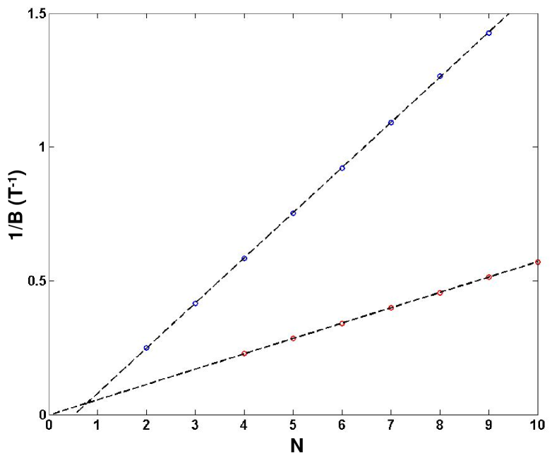
In order to compare the Kane-model calculations with the experimental data, the density of states (DOS) at the Fermi level was calculated from the Landau level spectrum (see Ref. novik2005 for more details). The Shubnikov-de Haas (SdH) oscillations observed in the experiments are directly related to the oscillations of the DOS at the Fermi energy. In Fig. 5 the calculated DOS, broadened by convolution with a Gaussian with a width =1.2 meV, is displayed together with SdH data for three different values of the gate voltage. A very good agreement between experiment and theory is evident. For all three different gate voltages, we find that there are always two sets of minima in the oscillations, one deep and one shallow, which result from the two sets of Landau levels for opposite spin (cf. Eqs. (26) and (27)). We first make the obvious identification that the deep minima result from the Landau level splitting and the shallow minima from the spin splitting. It is now instructive to plot the inverse of the magnetic field value for the positions of the deep minima as a function of the number N associated with the deep minima of the oscillation, as done previously to demonstrate the implications of the Berry phase of the Dirac Hamiltonian for the quantum Hall effect in graphenenovoselov2005 . As shown in Fig. 6, we find that when V, a straight line fit to the data extrapolates to , while for V, the fit extrapolates to . This different behavior can be understood from the effective Hamiltonian (1) in the main text of the article. For V, the electron density is low and the Fermi energy is near the Dirac point. In this limit, the band dispersion is dominated by the linear term in wave vector and the deep minima correspond to the filling factors (the factor of 2 takes the spin into account). The intercept of the straight-line fit evidently corresponds to the filling factor , which explains the intercept. However, for V, the electron density is increased and the Fermi energy is far away from the Dirac point. Consequently, the linear term is no longer dominant and other terms, such as the quadratic ones, will come into play. In this limit, the system recovers the usual behavior of a two dimensional electron gas and the deep minima correspond to the filling factors , implying that the intercept occurs at . Note that in HgTe, in contrast with graphene, one always has additional shallow minima besides the deep ones due to the coexistence of the linear term and other type of terms, such as quadratic or Zeeman terms. Another important feature of the SdH oscillations in Fig. 5 is the appearance of a beating pattern when V, indicating the occurrence of Rashba spin splittingwinklerbook2003 , which from this data is estimated to be 2.5 meV. The beating feature is not observable when the gate voltage is in the range of 0 1 V, which indicates that the system becomes more symmetric for low electron densities. An extensive discussion of this effect can be found in Ref. rothe2010 .
VII.3 Calculation of the minimal conductivity
In this section of the supplementary material, we discuss details of the calculation of the minimal conductivity given by Eqs. (5) and (6) in the main part of the article.
We use the Kubo formula for the longitudinal () dc conductivity,
| (29) |
| (30) |
Here the velocity operator , spectral function and retarded/advanced Green’s functions are matrices in - subband space of the effective Hamiltonian described by Eqs. (1) and (2) of the main manuscript. We use the symbol () to designate the trace operation . The spin degree of freedom is accounted for by the factor of 2 in Eq. (29). is the Fermi function, is the energy measured from the neutrality point and is the wave vector in the plane of the quantum well (QW).
Our next step is to calculate the disorder-averaged Green’s functions . In the minimal conductivity regime the most relevant types of disorder in our HgTe QWs are the inhomogeneity of the carrier density and the spatial fluctuations of the QW thickness around critical value . The carrier density inhomogeneity induces random fluctuations of the electrostatic potential in the QW, which we treat as weak gaussian disorder with standard averaging procedures leading to the complex self-energy in the equation for (see, Eqs. (34) and (35) below). In this respect, we follow the previous theoretical work on graphene (see, e.g. Refs. Shon98 ; Ostrovsky06 ). The new feature of our model is that it also accounts for the QW thickness fluctuations which is a specific type of disorder in HgTe/CdTe structures. This type of disorder induces sizable regions in the sample where the effective Dirac mass has small positive or negative values :
| (31) |
where meVnm-1 is a proportionality coefficient that we determine from band structure calculations. We assume that the gap varies slowly between the regions with and in the sense that the carrier motion adiabatically adjusts to the variation of . Both and its gradient are supposed to vanish upon averaging over the whole sample area () so that the leading nonzero moment of is the variance:
| (32) |
In view of the adiabatic dependence it is convenient to use the mixed representation for the Green’s functions defined by the Wigner transformation:
| (33) |
where satisfies the equation:
| (34) |
Here we omit the corrections to the linear Dirac Hamiltonian [see Eqs. (1) and (2) for in the main manuscript] because the main contribution to the minimal conductivity comes from the vicinity of the point ( is the Fermi energy measured from the neutrality point). For the same reason, in Eq. (34) the self-energy (generated by the random potential fluctuations) is taken at . It has been established earlier that the universal minimal conductivity follows already from the self-consistent Born approximation or equivalent approaches (e.g. Refs. Fradkin86b ; Ludwig94 ; Shon98 ; Ostrovsky06 ). We also adopt this approximation for the self-energy:
| (35) |
where is the Fourier transform of the correlation function of the random potential, which is an even function of the wave-vector due to the statistical homogeneity of the disorder.
In order to solve Eq. (34) we follow the same strategy as in the case of the uniform , i.e. we first apply operator to both sides of the equation from the left. Since does not commute with and , there appear additional gradient terms which are absent if :
| (36) | |||
We are interested in the average Green’s function over the sample area: and, respectively, . Upon such averaging the linear terms , and in Eq. (36) vanish, while the quadratic term does not. The latter is assumed to vary slowly in space, allowing us to neglect the corrections and to obtain the following equations for the Green’s function and the self-energy:
| (37) |
These results are justified if the average slope of the gap variation, , is small compared to the characteristic electron wave-number ,
| (38) |
where is the spectral broadening due to the finite elastic life-time. It eliminates the infrared divergence of the integral in Kubo formula (29), providing an effective cut-off at small values of .
We now use Eq. (37) for and to calculate the integral in Eq. (29) and express the conductivity in the form:
| (39) |
| (40) | |||||
For Eq. (40) yields the zero-temperature minimal conductivity . To completely specify Eq. (40) we find the self-energy from Eq. (37) in the form of a power-law expansion:
| (41) |
Assuming and a cutoff meV at high energies [where the quadratic term becomes comparable with the linear one in ], we obtain the expansion coefficients asfootnotelimits
| (42) | |||
| (43) |
This model adequately describes the observed minimal conductivity and its temperature dependence. In particular, at low temperatures the -dependence is quadratic:
| (44) |
At the conductivity becomes approximately linear as a manifestation of the linear density of states of the 2D Dirac fermions in HgTe QWs. The fit to the experimental curve in Fig. 4b is achieved for meV and .
References
- (1) Semenoff, G. W. Condensed-Matter simulation of a Three-Dimensional anomaly. Phys. Rev. Lett. 53, 2449–2452 (1984).
- (2) diVincenzo, D. P. & Mele, E. J. Self-consistent effective-mass theory for intralayer screening in graphite intercalation compounds. Phys. Rev. B 29, 1685–1694 (1984).
- (3) Castro Neto, A. H., Guinea, F., Peres, N. M. R., Novoselov, K. S. & Geim, A. K. The electronic properties of graphene. Reviews of Modern Physics 81, 109 (2009).
- (4) B. A. Bernevig, T. L. Hughes & S.C. Zhang. Quantum spin hall effect and topological phase transition in hgte quantum wells. Science 314, 1757 (2006).
- (5) König, M. et al. Quantum spin hall insulator state in hgte quantum wells. Science 318, 766–770 (2007).
- (6) König, M. et al. The quantum spin hall effect: Theory and experiment. J. Phys. Soc. Japan 77, 031007 (2008).
- (7) Wu, C., Bernevig, B. A. & Zhang, S.-C. Helical liquid and the edge of quantum spin hall systems. Phys. Rev. Lett. 96, 106401 (2006).
- (8) Nielsen, H. B. & Ninomiya, M. Absence of neutrinos on a lattice : (i). proof by homotopy theory. Nucl. Phys. B 185, 20–40 (1981).
- (9) Note that it is possible to have a single Dirac cone on the two dimensional surface of a three dimensional topological insulator. While the recently discovered materials Bi2Se3 and Bi2Te3 provide such examplesxia2009 ; chen2009 , sample quality has so far not been sufficient to perform high resolution transport experiments. Alternatively, massless Dirac fermions could also be realized at the two dimensional interface between different three dimensional semiconductors, although experimental realizations have not yet been foundpankratov1990 .
- (10) Roth, A. et al. Nonlocal transport in the quantum spin hall state. Science 325, 294–297 (2009).
- (11) Stahl, A. Ph.D. Thesis, University of Würzburg, Germany, 2010.
- (12) Hinz, J. et al. Gate control of the giant rashba effect in hgte quantum wells. Semiconductor Science and Technology 21, 501 (2006).
- (13) Jackiw, R. Fractional charge and zero modes for planar systems in a magnetic field. Phys. Rev. D 29, 2375 (1984).
- (14) Novoselov, K. S. et al. Two-dimensional gas of massless dirac fermions in graphene. Nature 438, 197–200 (2005).
- (15) Zhang, Y., Tan, Y., Stormer, H. L. & Kim, P. Experimental observation of the quantum hall effect and berry’s phase in graphene. Nature 438, 201–204 (2005).
- (16) Novik, E. G. et al. Band structure of semimagnetic quantum wells. Phys. Rev. B 72, 035321 (2005).
- (17) Rothe, D. G. et al. Fingerprint of different spin corbit terms for spin transport in HgTe quantum wells. New Journal of Physics 12, 065012 (2010).
- (18) Bolotin, K. et al. Ultrahigh electron mobility in suspended graphene. Solid State Communications 146, 351–355 (2008).
- (19) Fradkin, E. Critical behavior of disordered degenerate semiconductors. II. spectrum and transport properties in mean-field theory. Phys. Rev. B 33, 3263 (1986).
- (20) Tworzydło, J., Trauzettel, B., Titov, M., Rycerz, A. & Beenakker, C. W. J. Sub-poissonian shot noise in graphene. Phys. Rev. Lett. 96, 246802 (2006).
- (21) Du, X., Skachko, I., Barker, A. & Andrei, E. Y. Approaching ballistic transport in suspended graphene. Nat Nanotechn. 3, 491–495 (2008).
- (22) Winkler, R. Spin-orbit coupling effects in two-dimensional electron and hole systems. Springer Tracts in Modern Physics, 2003.
- (23) Shon, N. H. & Ando, T. Quantum transport in Two-Dimensional graphite system. J. Phys. Soc. Japan 67, 2421–2429 (1998).
- (24) Ostrovsky, P. M., Gornyi, I. V. & Mirlin, A. D. Electron transport in disordered graphene. Phys. Rev. B 74, 235443 (2006).
- (25) Ludwig, A. W. W., Fisher, M. P. A., Shankar, R. & Grinstein, G. Integer quantum hall transition: An alternative approach and exact results. Phys. Rev. B 50, 7526–7552 (1994).
- (26) In the appropriate limits Eqs. (42) and (43) coincide with the results obtained for graphene in Ref. Ostrovsky06 .
- (27) Xia, Y. et al. Observation of a large-gap topological-insulator class with a single dirac cone on the surface. Nat Phys 5, 398–402 (2009).
- (28) Chen, Y. L. et al. Experimental realization of a Three-Dimensional topological insulator, Bi2Te3. Science 325, 178–181 (2009).
- (29) Pankratov, O. A. Electronic properties of band-inverted heterojunctions: supersymmetry in narrow-gap semiconductors. Semiconductor Science and Technology 5, S204 (1990).