Rewritable nanoscale oxide photodetector
Nanophotonic devices seek to generate, guide, and/or detect light using structures whose nanoscale dimensions are closely tied to their functionality.(Sirbuly et al., 2005; Agarwal and Lieber, 2006) Semiconducting nanowires, grown with tailored optoelectronic properties, have been successfully placed into devices for a variety of applications.(Wang et al., 2001; Tian et al., 2007; Fan et al., 2008) However, the integration of photonic nanostructures with electronic circuitry has always been one of the most challenging aspects of device development. Here we report the development of rewritable nanoscale photodetectors created at the interface between LaAlO3 and SrTiO3. Nanowire junctions with characteristic dimensions 2-3 nm are created using a reversible AFM writing technique.(Cen et al., 2008, 2009) These nanoscale devices exhibit a remarkably high gain for their size, in part because of the large electric fields produced in the gap region. The photoconductive response is gate-tunable and spans the visible-to-near-infrared regime. The ability to integrate rewritable nanoscale photodetectors with nanowires and transistors in a single materials platform foreshadows new families of integrated optoelectronic devices and applications.
The discovery of a quasi two-dimensional electron gas (q-2DEG) at the interface between insulating oxides(Ohtomo and Hwang, 2004) has accelerated interest in oxide-based electronics.(Mannhart et al., 2008) The interface between LaAlO3 and SrTiO3 undergoes an abrupt insulator-to-metal transition as a function of the number of LaAlO3 layers;(Thiel et al., 2006) for structures at or near the critical thickness ( unit cells), the conductance becomes highly sensitive to applied electric fields.(Thiel et al., 2006) By applying the electric field locally using a conducting AFM probe, one can control this metal-insulator transition with resolution approaching one nanometer.(Cen et al., 2008, 2009) Devices such as rectifying junctions(Bogorin et al., 2009) and transistors(Cen et al., 2009) can be created, modified, and erased with extreme nanoscale precision. Additionally, as LaAlO3 and SrTiO3 are both wide-bandgap insulators they are essentially transparent at visible wavelengths, making it an interesting material system on which to search for photonic functionality.
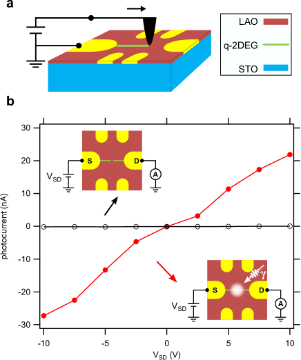
In this letter we demonstrate the creation of nanophotonic devices at the LaAlO3/SrTiO3 interface using conducting-AFM lithography (Figure 1a). Oxide heterostructures, consisting of 3 units cells of LaAlO3 on TiO2-terminated SrTiO3 (ref. Kawasaki et al., 1994), are grown by pulsed-laser deposition (see the Supplementary Information for details about growth conditions). Following contact to the interface with low-resistance Au electrodes, nanostructures are created at the LaAlO3/SrTiO3 interface by applying positive voltages to a conducting AFM tip. Nanoscale insulating gaps are formed by “cutting” these nanowires with a negatively-biased AFM tip that passes over the nanowire. Electronic nanostructures can be created with a high degree of precision and, furthermore, are relocatable and reconfigurable.
The nanostructures are characterized by applying a voltage bias to a “source” electrode () and then measuring the current from a “drain” electrode (). Optical properties are measured by illuminating the sample with laser light; when the light overlaps with the device a sharp increase in the conductance is observed. A small, persistent photoconductive effect is observed under continuous illumination (Supplementary Figure 4). These background effects are removed by modulating the laser intensity at frequency using an optical chopper. The resulting photocurrent, , is detected with a lock-in amplifier at . Figure 1b shows a typical photocurrent response as a function of . The photoconductive properties of these nanodevices are mapped spatially using scanning photocurrent microscopy (SPCM).(Balasubramanian et al., 2005) A microscope objective ( or 0.73) mounted to a closed-loop, three axis piezo scanner focuses the light and raster-scans it relative to the sample surface. The resulting photocurrent is measured as a function of laser position. To maximize nanostructure lifetimes,(Cen et al., 2009) measurements are performed in a vacuum of mbar. To reduce the signal from thermally-activated carriers, some experiments are performed in a continuous-flow cryostat at K.
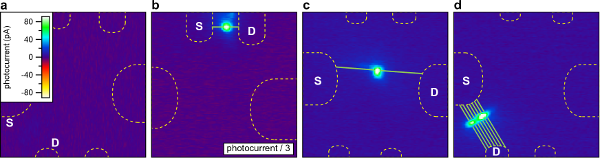
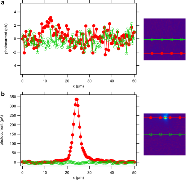
The photosensitivity of the devices written at the LaAlO3/SrTiO3 interface is spatially localized near the gap regions. An SPCM image of the photocurrent between two electrodes that do not have a device written between them shows a spatially diffuse photocurrent of less than 2 pA (Figure 2a and Supplementary Figure 6). The simplest nanophotonic device consists of a nanowire with a narrow gap or junction. This device is created by first writing the wire with an AFM tip bias of V, producing a nanowire with width nm (Supplementary Figure 1); the junction is created by crossing the wire with V, producing a gap with comparable width nm. The nanowire junctions can be deterministically placed with nanometer-scale accuracy. The SPCM image shows localized photocurrent ( nm and K) detected in the region of the junction (Figure 2b). The devices are erasable and reconfigurable: after measuring the device shown in Figure 2b, the device was erased and a new device was created farther from the electrodes (Figure 2c). The photosensitivity of these devices can be optically modulated at frequencies as high as 3.5 kHz and the response appears to be limited by the RC time constant of the device (see the Supplementary Information).
More complex devices are readily created: a nanowire junction array (Figure 2d) consisting of seven parallel wires spaced 2 µm apart is drawn between the source and drain electrodes. The nanowires are subsequently cut in a single stroke using a tip bias of V, creating neighboring junctions of width nm. The resulting photocurrent image shows the expected stripe shape, demonstrating that the photocurrent signal originates from all of the gaps. Even though the focused spot size ( µm) is smaller than the line spacing, the individual junctions are not separately distinguished. The photocurrent at the interior junction is suppressed compared to the outermost junctions due to the electrical screening by the nanowires. This result indicates how carrier diffusion away from the junctions can also contribute significantly to the overall photocurrent response. The extent of the photoconductive spatial sensitivity appears to be of the order of the spacing in this case ( µm).
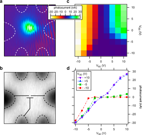
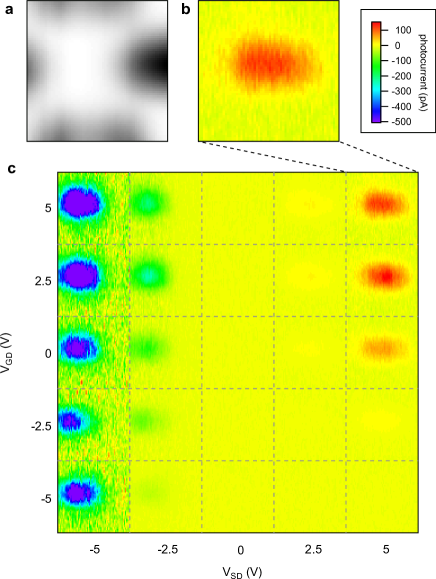
The functionality of these devices can be extended by adding an independent gate electrode. Here, we adopt a geometry previously investigated as a nanoscale transistor, i.e., a “SketchFET”(Cen et al., 2009). The “gate” electrode is written perpendicular to the existing source-drain nanowire (Supplementary Figure 2). This bias can be used to modify the source-drain conductance, enabling conduction between source and drain for positive and inhibiting it for negative . As for the two-terminal wire with junction, photocurrent that is spatially localized near the junction is observed where the device was written (Figure 3a). A simultaneously acquired laser reflectivity image (Figure 3b) does not show any observed signature of the nanophotonic detector, such as changes in the absorption or scattering, which is also the case for two-terminal devices. SPCM images are acquired for an array of source and gate biases, (Supplementary Figure 5). The photocurrent, measured as a function of and (Figure 3c.) exhibits a polarity that is always the same sign as the , irrespective of , indicating that there is negligible leakage current from the gate to the drain. Furthermore, the photocurrent is suppressed when both is positive and is negative, demonstrating the ability of the gate electrode to tune the photoconductivity in the source-drain channel.
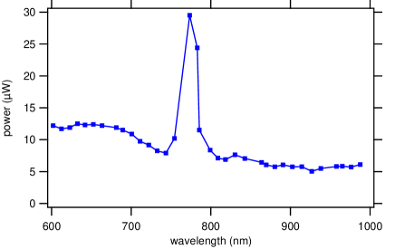
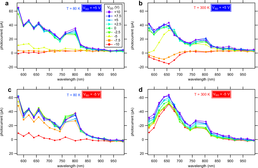
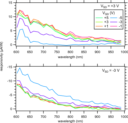
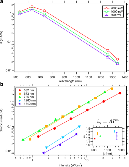
To investigate the wavelength dependence of these devices, a pulsed, mode-locked Ti:Sapphire laser is focused into a photonic crystal fiber to provide tunable laser illumination over the continuous wavelength range nm (ref. Dudley et al., 2006). As the white light source power varies with wavelength (Supplementary Figure 8) the normalized responsivity of the device (, where is the laser power) is shown over this wavelength range (Figure 4). Data points in the vicinity of the pulsed laser source ( nm) are not shown because of the high peak power and nonlinear effects in the sample (Figure 5). The spectral response is sensitive to and . At positive the photodetector response red-shifts as the gate bias is increased. The tuning of the responsivity is enhanced for positive , which is consistent with the behavior demonstrated in Figure 3. Measurements taken as a function of temperature (Supplementary Figure 9) show a slight red-shift with increasing temperature.
In addition to the supercontinuum white light source, the optical response is measured at a number of fixed wavelengths ranging from the visible to near-infrared: 532 nm, 633 nm, 735 nm, 1260 nm, and 1340 nm. The response at these wavelengths is consistent with the supercontinuum measurement in the range 6001000 nm (Figure 5a). Remarkably, the photosensitivity extends to 1340 nm, the longest wavelength investigated. A three-terminal device has similar tuning behavior from and at 1340 nm and at visible wavelengths (Supplementary Figure 7). The intensity dependence of the photocurrent exhibits power-law behavior (Figure 5b), , where is the photocurrent, is a proportionality constant, is the laser intensity, and 1.21.4. The super-linear scaling with laser intensity is similar to other systems that are near a metal-insulator transition.(Stöckmann, 1969; Prezioso et al., 2009)
There are several possible mechanisms for the photoconductivity. The direct and indirect bandgaps of SrTiO3 (3.75 eV and 3.25 eV, respectively(van Benthem et al., 2001)) are too large to explain the visible to near-infrared photoresponse. Above-band photoexcitation of SrTiO3 can produce excitonic luminescence at visible wavelengths, indicating the existence of mid-gap states.(Grabner, 1969; Leonelli and Brebner, 1986; Okamura et al., 2006) The most readily formed mid-gap states are associated with oxygen vacancies, which are known to form during substrate preparation(Kawasaki et al., 1994; Kareev et al., 2008; Zhang et al., 2008) and growth of LaAlO3/SrTiO3 heterostructures.(Herranz et al., 2007; Kalabukhov et al., 2007; Basletic et al., 2008; Seo et al., 2009) Localized states just below the conduction band have been probed via transport in SrTiO3-based field-effect devices.(Shibuya et al., 2007) Unintentional doping of SrTiO3 substrates (e.g, Cr, Fe, or Al) can also contribute states within the bandgap.(Feng, 1982)
Electrons occupying mid-gap states can be optically excited into the conduction band using sub-bandgap light. The photoexcited electrons are swept across the junction by the large electric field ( MV/cm), resulting in photocurrent. The spectral sensitivity we observe (Figures 4, 5, and Supplemental Figure 9) is consistent with previous optical measurements on oxygen vacancy-rich samples.(Kalabukhov et al., 2007; Kareev et al., 2008; Zhang et al., 2008; Seo et al., 2009) Along the nanowire and sufficiently far from the gap, photo-induced current is negligible because the electric fields are screened or otherwise sufficiently small.
The rewritable photodetectors presented here bring new functionality to oxide nanoelectronics. For example, existing nanowire-based molecular sensors(Cui et al., 2001) rely on the ability to bring the analyte into contact with the sensing area of the detector. Here the roles are reversed: a nanoscale photodetector can be placed in intimate contact with an existing molecule or biological agent. The ability to integrate optical and electrical components such as nanowires and transistors may lead to devices that combine in a single platform sub-wavelength optical detection with higher-level electronics-based information processing.
Acknowledgements.
The authors gratefully acknowledge financial support from DARPA (W911N3-09-10258) (J.L.) the Fine Foundation (J.L.), and the National Science Foundation through grants DMR-0704022 (J.L.) and DMR-0906443 (C.B.E).References
- Sirbuly et al. (2005) D. J. Sirbuly, M. Law, H. Yan, and P. Yang, J. Phys. Chem. B 109, 15190 (2005).
- Agarwal and Lieber (2006) R. Agarwal and C. M. Lieber, Appl. Phys. A: Mater. 85, 209 (2006).
- Wang et al. (2001) J. Wang, M. S. Gudiksen, X. Duan, Y. Cui, and C. M. Lieber, Science 293, 1455 (2001).
- Tian et al. (2007) B. Tian, X. Zheng, T. J. Kempa, Y. Fang, N. Yu, G. Yu, J. Huang, and C. M. Lieber, Nature 449, 885 (2007).
- Fan et al. (2008) Z. Fan, J. C. Ho, Z. A. Jacobson, H. Razavi, and A. Javey, P. Nat. Acad. Sci. (USA) 105, 11066 (2008).
- Cen et al. (2008) C. Cen, S. Thiel, G. Hammerl, C. W. Schneider, K. E. Andersen, C. S. Hellberg, J. Mannhart, and J. Levy, Nature Mater. 7, 298 (2008).
- Cen et al. (2009) C. Cen, S. Thiel, J. Mannhart, and J. Levy, Science 323, 1026 (2009).
- Ohtomo and Hwang (2004) A. Ohtomo and H. Y. Hwang, Nature 427, 423 (2004).
- Mannhart et al. (2008) J. Mannhart, D. Blank, H. Hwang, A. Millis, and J.-M. Triscone, MRS Bull. 33, 1027 (2008).
- Thiel et al. (2006) S. Thiel, G. Hammerl, A. Schmehl, C. W. Schneider, and J. Mannhart, Science 313, 1942 (2006).
- Bogorin et al. (2009) D. F. Bogorin, C. W. Bark, H. W. Jang, C. Cen, C.-B. Eom, and J. Levy, Appl. Phys. Lett 97, 013102 (2009), arXiv:0912.3714v1 .
- Kawasaki et al. (1994) M. Kawasaki, K. Takahashi, T. Maeda, R. Tsuchiya, M. Shinohara, O. Ishiyama, T. Yonezawa, M. Yoshimoto, and H. Koinuma, Science 266, 1540 (1994).
- Balasubramanian et al. (2005) K. Balasubramanian, M. Burghard, K. Kern, M. Scolari, and A. Mews, Nano Lett. 5, 507 (2005).
- Dudley et al. (2006) J. M. Dudley, G. Genty, and S. Coen, Rev. Mod. Phys. 78, 1135 (2006).
- Stöckmann (1969) F. Stöckmann, Phys. Stat. Sol. 34, 751 (1969).
- Prezioso et al. (2009) S. Prezioso, S. M. Hossain, A. Anopchenko, L. Pavesi, M. Wang, G. Pucker, and P. Bellutti, Appl. Phys. Lett. 94, 062108 (2009).
- van Benthem et al. (2001) K. van Benthem, C. Elsasser, and R. H. French, J. App. Phys. 90, 6156 (2001).
- Grabner (1969) L. Grabner, Phys. Rev. 177, 1315 (1969).
- Leonelli and Brebner (1986) R. Leonelli and J. L. Brebner, Phys. Rev. B 33, 8649 (1986).
- Okamura et al. (2006) H. Okamura, M. Matsubara, K. Tanaka, K. Fukui, M. Terakami, H. Nakagawa, Y. Ikemoto, T. Moriwaki, H. Kimura, and T. Nanba, J. Phys. Soc. Jpn. 75, 023703 (2006).
- Kareev et al. (2008) M. Kareev, S. Prosandeev, J. Liu, A. Kareev, J. W. Freeland, M. Xio, and J. Chakhalian, Appl. Phys. Lett. 93, 061909 (2008).
- Zhang et al. (2008) J. Zhang, S. Walsh, C. Brooks, D. G. Schlom, and L. J. Brillson, J. Vac. Sci. Technol. B 26, 1466 (2008).
- Herranz et al. (2007) G. Herranz, M. Basletić, M. Bibes, C. Carrétéro, E. Tafra, E. Jacquet, K. Bouzehouane, C. Deranlot, A. Hamzić, J.-M. Broto, A. Barthélémy, and A. Fert, Phys. Rev. Lett. 98, 216803 (2007).
- Kalabukhov et al. (2007) A. Kalabukhov, R. Gunnarsson, J. Borjesson, E. Olsson, T. Claeson, and D. Winkler, Phys. Rev. B 75, 121404 (2007).
- Basletic et al. (2008) M. Basletic, J. Maurice, C. Carretero, G. Herranz, O. Copie, M. Bibes, E. Jacquet, K. Bouzehouane, S. Fusil, and A. Barthelemy, Nature Mater. 7, 621 (2008).
- Seo et al. (2009) S. S. A. Seo, Z. Marton, W. S. Choi, G. W. J. Hassink, D. H. A. Blank, H. Y. Hwang, T. W. Noh, T. Egami, and H. N. Lee, Appl. Phys. Lett. 95, 082107 (2009).
- Shibuya et al. (2007) K. Shibuya, T. Ohnishi, T. Sato, and M. Lippmaa, J. App. Phys. 102, 083713 (2007).
- Feng (1982) T. Feng, Phys. Rev. B 25, 627 (1982).
- Cui et al. (2001) Y. Cui, Q. Wei, H. Park, and C. M. Lieber, Science 293, 1289 (2001).
Rewritable nanoscale oxide photodetector: Supplementary Information
Patrick Irvin,1 Yanjun Ma,1 Daniela F. Bogorin,1 Cheng Cen,1 Chung
Wung Bark,2 Chad M. Folkman,2 Chang-Beom Eom,2 and Jeremy Levy1
1Department of Physics and Astronomy,
University of Pittsburgh, Pittsburgh, Pennsylvania 15260
2Department of Materials Science and Engineering,
University of Wisconsin-Madison, Madison, Wisconsin 53706
Material Growth and Device Preparation
Oxide heterostructures are grown by pulsed laser deposition with in situ high pressure RHEED. Low miscut () (001) SrTiO3 substrates are treated by a modified BHF etch and annealed in oxygen at 1000∘C for 2 hours to produce a TiO2-terminated and atomically smooth surface with single unit cell (uc) steps, as verified by AFM inspection. Thin (3 uc) layers of LaAlO3 are deposited on SrTiO3 at a temperature of C and oxygen pressure of mbar. A laser with energy density of 2 J/cm2 and repetition rate of 3 Hz is used to ablate the LaAlO3 single crystal target.
In order to probe the interface of LaAlO3 and SrTiO3, low-resistance electrodes are contacted directly to the q-2DEG. Argon ion beam etching is used to mill nm deep into the SrTiO3. Electrodes are then formed by first sputter-depositing a 2 nm Ti adhesion layer followed by nm of Au into the etched region.
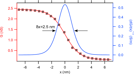
Wires with width nm are written using an Asylum MFP-3D AFM in contact mode. A positive bias voltage applied to the tip creates conducting nanoregions directly below the AFM tip, while negative voltages locally restore the insulating state. Nanostructures are created under normal atmospheric conditions at room temperature; the AFM is kept in a dark environment to suppress photoconduction in the SrTiO3 substrate ( eV). The conductivity of the q-2DEG is monitored with a Keithley picoammeter while writing: when the wire is connected to both electrodes, a sharp increase in conductance is observed. Similarly, the conductance is monitored while cutting a wire. The distance over which the conductance drops is used to quantify the wire width (Cen et al., 2008), as shown in Supplementary Figure 1. Writing and erasing of nanowires is reproducible for a given tip bias and oxide heterostructure.
Optical Modulation
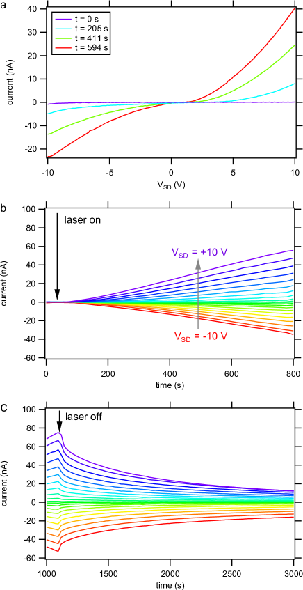
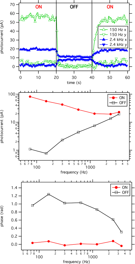
The photosensitivity of these devices can be optically modulated at frequencies as high as 3.5 kHz, as shown in Supplementary Figure 4. The phase of the photocurrent is constant over the frequency range probed while under illumination (ie, the “on” state). In this case the light lowers the resistance of the detector. The frequency response of the device is limited by the RC time constant of the junction. When the laser light is blocked (“off”), the detector is in a high resistance state. In the off state we observe a phase shift as the frequency is increased (Supplementary Figure 4), indicating we are indeed limited by the resistance.
Scanning Photocurrent Microscopy Image Analysis
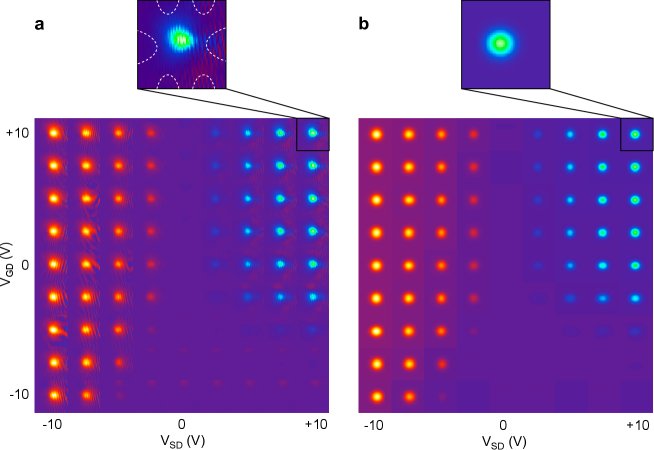
In order to extract a value for the photocurrent from a SPCM image, the image is fit to a two-dimensional Gaussian of the form
where is the image offset, is the amplitude of the 2D peak, and are the peak offsets, and and are the peak widths. We then define the photocurrent as .