Anomalously strong pinning of the filling factor in epitaxial graphene
Abstract
We explore the robust quantization of the Hall resistance in epitaxial graphene grown on Si-terminated SiC. Uniquely to this system, the dominance of quantum over classical capacitance in the charge transfer between the substrate and graphene is such that Landau levels (in particular, the one at exactly zero energy) remain completely filled over an extraordinarily broad range of magnetic fields. One important implication of this pinning of the filling factor is that the system can sustain a very high nondissipative current. This makes epitaxial graphene ideally suited for quantum resistance metrology, and we have achieved a precision of 3 parts in in the Hall resistance quantization measurements.
pacs:
73.43.-f,72.80.Vp,06.20.F-The quantum Hall effect (QHE) is one of the key fundamental phenomena in solid-state physics Klitzing et al. (1980). It was observed in two-dimensional electron systems in semiconductor materials and, since recently, in graphene: both in exfoliated Novoselov et al. (2005); Zhang et al. (2005); Castro Neto et al. (2009) and epitaxial Shen et al. (2009); Wu et al. (2009); Tzalenchuk et al. (2010); Jobst et al. (2010); Tanabe et al. (2010) devices. A direct high-accuracy comparison of the conventional QHE in semiconductors with that observed in graphene constitutes a test of the universality of this effect. The affirmative result would strongly support the pending redefinition of the SI units based on the Planck constant and the electron charge Mills et al. (2006) and provide an international resistance standard based upon quantum physics Jeckelmann and Jeanneret (2001).
Graphene is believed to offer an excellent platform for QHE metrology due to the large energy separation between Landau levels (LL) resulting from the Dirac-type “massless” electrons specific for its band structure Geim (2009). The Hall resistance quantization with an accuracy of 3 parts in has already been established Tzalenchuk et al. (2010) in Hall-bar devices manufactured from epitaxial graphene grown on Si-terminated face of SiC (SiC/G). However, for graphene to be practically employed as an embodiment of a quantum resistance standard, it needs to satisfy further stringent requirements Jeckelmann and Jeanneret (2001), in particular with respect to robustness over a range of temperature, magnetic field and measurement current. A high measurement current, which a device can sustain at a given temperature without dissipation, is particularly important for precision metrology as it defines the maximum attainable signal-to-noise ratio.
The extent of the QHE plateaux in conventional 2D electron systems is, usually, set by disorder and temperature. Disorder pins the Fermi energy in the mobility gap of the 2D system, which suppresses dissipative transport at low temperatures over a finite range of magnetic fields around the values corresponding to exactly filled LLs. These values can be calculated from the carrier density determined from the low-field Hall resistivity measurements and coincide with the maximum non-dissipative current, the breakdown current. Thus, the breakdown current in conventional two-dimensional semicondutors peaks very close to the field values where the filling factor is an even integer Jeckelmann and Jeanneret (2001). Though less studied experimentally, the behaviour of the breakdown current on the plateaux for the exfoliated graphene, including the plateau corresponding to the topologically protected LL, looks quite similar Bennaceur et al. (2010).
In this Brief Report we explore the robustness of the Hall resistance quantization in SiC/G. Unlike the QHE in conventional 2D systems, where the carrier density is independent of magnetic field, here specifically to SiC/G, we find that the carrier density in graphene varies with magnetic field due to the charge transfer between surface donor states in SiC and graphene. Most importantly, we find magnetic field intervals of several Tesla, where the carrier density in graphene increases linearly with the magnetic field, resulting in the pinning of state with electrons at the the chemical potential occupying SiC surface donor states half-way between the and LLs in graphene. Interestingly, at magnetic fields above the filling factor pinning interval, the carrier density saturates at a value up to 30% higher than the zero-field carrier density. The pinned filling factor manifests itself in a continuously increasing breakdown current toward the upper magnetic field end of the state far beyond the nominal value of calculated from the zero-field carrier density. Facilitated by the high breakdown current in excess of 500 at 14 T we have achieved a precision of 3 parts in in the Hall resistance quantization measurements.
The anomalous pinning of filling factors in SiC/G is determined by the dominance of the quantum capacitance, , Luryi (1988) over the classical capacitance per unit area, , in the charge transfer between graphene and surface-donor states of SiC/G: , where , and is the density of states of electrons at the Fermi level. The latter reside in the ’dead layer’ of carbon atoms, just underneath graphene van Bommel et al. (1975); Riedl et al. (2007); Varchon et al. (2007); Mattausch and Pankratov (2007); Emtsev et al. (2008); Qi et al. (2010). This layer is characterised by a supercell of the reconstructed surface of sublimated SiC. Missing or substituted carbon atoms in various positions of such a huge supercell in the dead layer create localised surface states with a broad distribution of energies within the bandgap of SiC ().
It appears that the density of such defects is higher in material grown at low temperatures () resulting in graphene doped to a large electron density, , which is difficult to change Kopylov et al. (2010). On the other hand, growth at higher temperatures, , and in a highly pressurised atmosphere of Ar seems to improve the integrity of the reconstructed ’dead’ layer, leading to a lower density of donors on the surface and, therefore, producing graphene with a much lower initial doping Tzalenchuk et al. (2010); Lara-Avila et al. (2011).
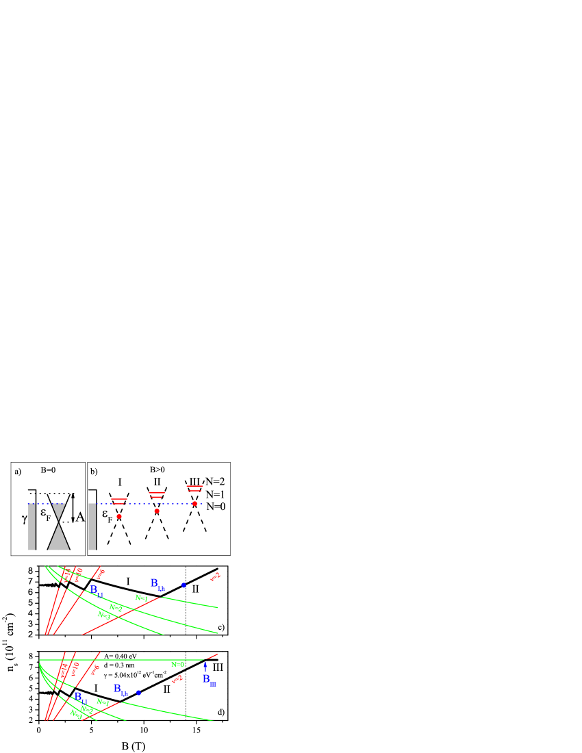
The quantum capacitance of a two-dimensional electron system is the result of a low compressibility of the electron liquid determined by the peaks in . For electrons in high-mobility GaAs/AlGaAs heterostructures in magnetic field, the quantum capacitance manifests itself in weak magneto-oscillations of the electron density Eisenstein et al. (1994); John et al. (2004) due to the suppressed density of states inside the inter-Landau level gaps. A similarly weak effect has been observed in graphene exfoliated onto n-Si/SiO2 substrate Ponomarenko et al. (2010), where the influence of a larger (than in usual semiconductors) inter-LL gaps is hindered by a strong charging effect determined by a relatively large thickness of SiO2 layer. For epitaxial graphene on SiC, due to the short distance, nm, between the dead layer hosting the donors and graphene, the effect of quantum capacitance is much stronger, and the oscillations of electron density take the form of the robust pinning of the electron filling factor. A similar behaviour was observed in STM spectroscopy of turbostratic graphite, where charge is transferred between the top graphene layer and the underlying bulk layers Song et al. (2010). The charge transfer in SiC/G is illustrated in the sketches in Fig. 1, for (a) and quantising magnetic fields (b). The transfer can be described using the charge balance equation Kopylov et al. (2010)
| (1) |
The left hand side of this equation accounts for the depletion of the surface donor states, where is the difference between the work function of undoped graphene and the work function of electrons in the surface donors in SiC, is the Fermi energy of electrons in graphene, and is the density of donor states in the dead layer. An amount, , of this charge density is transferred to graphene, and an amount, , (controlled by the gate voltage) - to the polymer gate Lara-Avila et al. (2011).
Graphical solutions for the charge transfer problem for two values of are shown in Fig. 1 (c) and 1(d) for a broad range of magnetic fields. For graphene within interval III (visible only in the case of the higher ) the Fermi energy coincides with the partially filled zero-energy LL, , which determines the carrier density , and can be up to 30% higher than the zero-field density in the same device Kopylov et al. (2010). This regime of fixed electron density is terminated at the low field end, at , where the LL is completely occupied by electrons with the density . Note that for the presented here, – the maximum field in our setup. Similarly, for magnetic field interval I, the Fermi level coincides with the partially filled LL (), and, for this interval, with . The interval I is limited by the field values for which the LL in the electron gas with the density is emptied at the higher field end, , and is full at the lower end, . In magnetic field interval II the chemical potential in the system lies inside the gap between and LL in graphene. As a result, over this entire interval the LL in graphene is full and is empty, so that the filling factor in graphene is fixed at the value , and the carrier density increases linearly with the magnetic field, , due to the charge transfer from SiC surface.
According to Eq. 1, lowering the carrier density using an electrostatic gate is equivalent to effectively reducing the work function difference between graphene and donor states by , which shifts the range of the magnetic fields where pinning of the state takes place. For instance, reducing the zero-field carrier density from [Fig. 1(c)] to [Fig. 1 (d)] moves interval II from down to , almost entirely within the experimental range.
In order to verify the predictions of the theory regarding the pinning of the filling factor and its implications for the resistance metrology, we studied the QHE in a polymer-gated epitaxial graphene sample with Hall bar geometry of width and length . Graphene was grown at and 1 atm Ar gas pressure on the Si-terminated face of a semi-insulating 4H-SiC(0001) substrate. The as-grown sample had the zero-field carrier density . Graphene was encapsulated in a polymer bilayer, a spacer polymer followed by an active polymer able to generate acceptor levels under UV light. At room temperature electrons diffuse from graphene through the spacer polymer layer and fill the acceptor levels in the top polymer layer. Such a photo-chemical gate allowed non-volatile control over the charge carrier density in graphene. More fabrication details can be found elsewhere Tzalenchuk et al. (2010); Lara-Avila et al. (2011).
Figure 2(a) shows magneto transport measurements on the encapsulated sample tuned to a zero-field carrier density of corresponding to the case in fig. 1(c)]. From the carrier density we estimate that the magnetic field needed for exact filling factor in this device is 13.8 T. A well-quantized Hall plateau in can be seen at for both magnetic field directions which is more than 5 T wide, whereas the longitudinal resistivity, , drops to zero signifying a non-dissipative state. In addition, a less precisely quantized plateau is present at , for which remains finite.
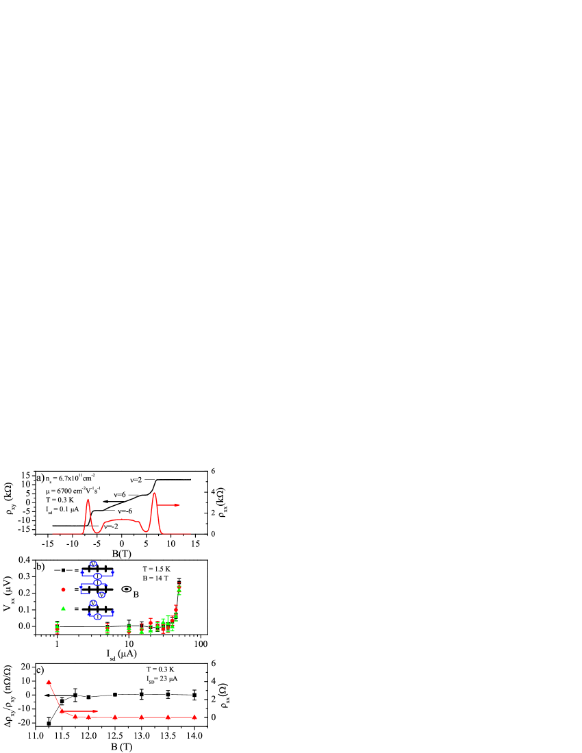
Accurate quantum Hall resistance measurements require that the longitudinal voltage remains zero (in practice, below the noise level of the nanovolt meter) to ensure the device is in the non-dissipative state, which can be violated by the breakdown of the QHE at high current. Figure 2(b) shows the determination of the breakdown current at on the plateau. Here we define as the source-drain current, , at which . We find for three different combinations of source-drain current contacts that the breakdown current for this value of is approximately (note that in a practical quantum Hall to resistance measurement is Williams et al. (2010)). The contact resistance, determined via a three-terminal measurement in the nondissipative state, is smaller than .
Figure 2(c) shows a precision measurement of and for different magnetic fields along the plateau. Note that this plateau appears much shorter in the magnetic field range than that shown in Fig. 2 (a) because of the 200 times larger measurement current used in precision measurements. From this figure we determine that the mean of is for the data between 11.75 and 14.0 T, while at the same time . This result represents an order of magnitude improvement of QHE precision measurements in graphene, as compared to the earlier record Tzalenchuk et al. (2010). Not only is QHE accurate, but it is also extremely robust in this epitaxial graphene device, easily meeting the stringent criteria for accurate quantum Hall resistance measurements normally applied to semiconductor systems.
Using the polymer gating method Lara-Avila et al. (2011), we further reduce the zero-field electron density in graphene to correspond to the solution of the charge transfer problem in Fig. 1(d), i.e. down to as evidenced by magnetotransport measurements in Fig. 3(a). On the quantum Hall resistance plateau we measure the breakdown current , defined above, as a function of the magnetic field. Unlike the conventional QHE materials Jeckelmann and Jeanneret (2001), the breakdown current in Fig. 3(a) continuously increases from zero to almost far beyond calculated from the zero-field carrier density. This is a direct consequence of the exchange of carriers between graphene and the donors in the ’dead’ layer, which keeps the LL completely filled well past .
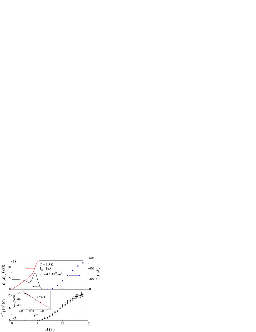
The magnetic field range where the Fermi energy in SiC/G lies half-way between the and LLs determines the activation energy for the dissipative transport. For such a high activation energy, the low-temperature dissipative transport is most likely to proceed through the variable range hopping (VRH) between surface donors in SiC involving virtual occupancy of the LL states in graphene to which they are weakly coupled. Indeed, as shown in the inset of Fig. 3(b), the temperature dependence of the conductivity measured at obeys an dependence typical of the VRH mechanism. The values determined from the measurements at different magnetic fields are plotted in the main panel of fig. 3(b). The breakdown current rising with field to very large values [Fig. 3(a)] corresponds to reaching extremely large values in excess of – at least an order of magnitude larger than that observed in GaAs Furlan (1998) and more recently in exfoliated graphene Giesbers et al. (2009); Bennaceur et al. (2010).
In conclusion, we have studied the robust Hall resistance quantization in a large epitaxial graphene sample grown on SiC. We have observed the pinning of the state which is consistent with our picture of magnetic field dependent charge transfer between the SiC surface and graphene layer. Together with the large break-down current this makes graphene on SiC the ideal system for high-precision resistance metrology.
Acknowledgements.
We are grateful to T. Seyller, A. Geim, K. Novoselov and K. von Klitzing for discussions. This work was supported by the NPL Strategic Research programme, Swedish Research Council and Foundation for Strategic Research, EU FP7 STREPs ConceptGraphene and SINGLE, EPSRC grant EP/G041954 and the Science & Innovation Award EP/G014787.References
- Klitzing et al. (1980) K. v. Klitzing, G. Dorda, and M. Pepper, Phys. Rev. Lett., 45, 494 (1980).
- Novoselov et al. (2005) K. S. Novoselov, A. K. Geim, S. V. Morozov, D. Jiang, M. I. Katsnelson, I. V. Grigorieva, S. V. Dubonos, and A. A. Firsov, Nature (London), 438, 197 (2005).
- Zhang et al. (2005) Y. B. Zhang, Y. W. Tan, H. L. Stormer, and P. Kim, Nature (London), 438, 201 (2005).
- Castro Neto et al. (2009) A. H. Castro Neto, F. Guinea, N. M. R. Peres, K. S. Novoselov, and A. K. Geim, Rev. Mod. Phys., 81, 109 (2009).
- Shen et al. (2009) T. Shen, J. J. Gu, M. Xu, Y. Q. Wu, M. L. Bolen, M. A. Capano, L. W. Engel, and P. D. Ye, Appl. Phys. Lett., 95 (2009).
- Wu et al. (2009) X. S. Wu, Y. K. Hu, M. Ruan, N. K. Madiomanana, J. Hankinson, M. Sprinkle, C. Berger, and W. A. de Heer, Appl. Phys. Lett., 95 (2009).
- Tzalenchuk et al. (2010) A. Tzalenchuk et al., Nature Nanotechnol., 5, 186 (2010).
- Jobst et al. (2010) J. Jobst, D. Waldmann, F. Speck, R. Hirner, D. K. Maude, T. Seyller, and H. B. Weber, Phys. Rev. B, 81 (2010).
- Tanabe et al. (2010) S. Tanabe, Y. Sekine, H. Kageshima, M. Nagase, and H. Hibino, Appl. Phys. Express, 3 (2010).
- Mills et al. (2006) I. M. Mills, P. J. Mohr, T. J. Quinn, B. N. Taylor, and E. R. Williams, Metrologia, 43, 227 (2006).
- Jeckelmann and Jeanneret (2001) B. Jeckelmann and B. Jeanneret, Rep. Prog. Phys., 64, 1603 (2001).
- Geim (2009) A. K. Geim, Science, 324, 1530 (2009).
- Bennaceur et al. (2010) K. Bennaceur, P. Jacques, F. Portier, P. Roche, and D. C. Glattli, (2010), arXiv:1009.1795v1 .
- Luryi (1988) S. Luryi, Appl. Phys. Lett., 52, 501 (1988).
- van Bommel et al. (1975) A. van Bommel, J. Crombeen, and A. van Tooren, Surf. Sci., 48, 463 (1975).
- Riedl et al. (2007) C. Riedl, U. Starke, J. Bernhardt, M. Franke, and K. Heinz, Phys. Rev. B, 76, 245406 (2007).
- Varchon et al. (2007) F. Varchon et al., Phys. Rev. Lett., 99 (2007).
- Mattausch and Pankratov (2007) A. Mattausch and O. Pankratov, Phys. Rev. Lett., 99 (2007).
- Emtsev et al. (2008) K. V. Emtsev, F. Speck, T. Seyller, L. Ley, and J. D. Riley, Phys. Rev. B, 77 (2008).
- Qi et al. (2010) Y. Qi, S. H. Rhim, G. F. Sun, M. Weinert, and L. Li, Phys. Rev. Lett., 105 (2010).
- Kopylov et al. (2010) S. Kopylov, A. Tzalenchuk, S. Kubatkin, and V. I. Fal’ko, Appl. Phys. Lett., 97 (2010).
- Lara-Avila et al. (2011) S. Lara-Avila, K. Moth-Poulsen, R. Yakimova, T. Bjornholm, V. Fal’ko, A. Tzalenchuk, and S. Kubatkin, Adv. Mater., 23, 878 (2011).
- Eisenstein et al. (1994) J. P. Eisenstein, L. N. Pfeiffer, and K. W. West, Phys. Rev. B, 50, 1760 (1994).
- John et al. (2004) D. L. John, L. C. Castro, and D. L. Pulfrey, J. Appl. Phys., 96, 5180 (2004).
- Ponomarenko et al. (2010) L. A. Ponomarenko, R. Yang, R. V. Gorbachev, P. Blake, A. S. Mayorov, K. S. Novoselov, M. I. Katsnelson, and A. K. Geim, Phys. Rev. Lett., 105 (2010).
- Song et al. (2010) Y. J. Song et al., Nature (London), 467, 185 (2010).
- Williams et al. (2010) J. M. Williams, T. J. B. M. Janssen, G. Rietveld, and E. Houtzager, Metrologia, 47, 167 (2010).
- Furlan (1998) M. Furlan, Phys. Rev. B, 57, 14818 (1998).
- Giesbers et al. (2009) A. J. M. Giesbers, U. Zeitler, L. A. Ponomarenko, R. Yang, K. S. Novoselov, A. K. Geim, and J. C. Maan, Phys. Rev. B, 80 (2009).