Fine structure and size dependence of exciton and bi-exciton optical spectra in CdSe nanocrystals
Abstract
Theory of electronic and optical properties of exciton and bi-exciton complexes confined in CdSe spherical nanocrystals is presented. The electron and hole states are computed using atomistic tight binding Hamiltonian including an effective crystal field splitting, spin-orbit interactions, and model surface passivation. The optically excited states are expanded in electron-hole configurations and the many-body spectrum is computed in the configuration-interaction approach. Results demonstrate that the low-energy electron spectrum is organized in shells (, , …), whilst the valence hole spectrum is composed of four low-lying, doubly degenerate states separated from the rest by a gap. As a result, the bi-exciton and exciton spectrum is composed of a manifold of closely lying states, resulting in a fine structure of exciton and bi-exciton spectra. The quasi-degenerate nature of the hole spectrum results in a correlated bi-exciton state, which makes it slowly convergent with basis size. We carry out a systematic study of the exciton and bi-exciton emission spectra as a function of the nanocrystal diameter and find that the interplay of repulsion between constituent excitons and correlation effects results in a change of the sign of bi-exciton binding energy from negative to positive at a critical nanocrystal size.
pacs:
78.67.Hc,78.67.Bf,73.21.La,71.35.-yI Introduction
Semiconductor nanocrystals (NCs) (Refs. klimov_arpc_2007, ; nair_geyer_prb08, ; gur_fromer_science05, ; nirmal_dabbousi_nature96, ; brus_nanolett2010, ; ekimov_hache_josa93, ; ellingson_beard_nanolett05, ; scholes_afm08, ; scholes_rumbles_natmat06, ; yu_wang_science03, ; pandey_guyot_jcp2007, ; gomez_califano_pccp06, ) are nano-sized crystalline particles with numbers of atoms of the order of -. NCs with controlled and tunable sizes as well as good optical properties are fabricated in a colloidal growth process.yin_alivisatos_nature05 This makes them excellent candidates for use in low-cost optoelectronic applications, including solar cells, biomarkers,fu_gu_con05 ; alivisatos_natbio_04 ; chan_nie_science98 light emitting diodes,colvin_schlam_nature94 ; dabbousi_bawendi_apl95 ; chanyawadee_lgoudakis_advmat09 photodetectors,konstantatos_sargent_natnano2010 ; sukhovatkin_hinds_science09 single-photon sources in quantum cryptography,pattantyus_qiao_nanolett09 or lasers.klimov_mikhaelovsky_science00 ; weisbuch_jcg94 In particular, it has been recently demonstrated that the optical gain in NCs can be blocked, created, and tuned by engineering the NC confinementklimov_ivanov_nature07 or the type of multiexciton complex active in the stimulated emission process.cooney_sewall_prl09
The NCs are considered as a promising material for the optically active media in solar cells. They offer a potential way to increase the efficiency of solar cells due to their tunable parameters amenable to optimization,hillhouse_beard_cocis09 ; wadia_alivisatos_est09 ; luther_law_nanolett08 ; choi_lim_nanolett09 ; johnston_pattantyus_apl08 as well as by generation of multi-exciton complexes (MEG) following absorption of a single high-energy photon.nozik_physE_2002 ; rabani_baer_nanolett08 ; schaller_pietryga_nanolett07 ; franceschetti_an_nanolett06 ; nair_bawendi_prb07 ; ellingson_beard_nanolett05 ; scholes_rumbles_natmat06 ; nozik_arpc01 During MEG a high-energy photon with energy of at least twice the semiconductor bandgap, , is absorbed creating an excited state, which can be described as a superposition of configurations with one and more electron-hole pairs.nozik_physE_2002 Alternatively, we can think of exciting a single exciton, which is then converted via Coulomb interactions into additional interacting electron-hole pairs. Energy relaxation of these multi-exciton complexes results in multiple carriers at the bottom of the conduction and the top of the valence bands. These multi-exciton states decay into exciton states by Auger processes, limiting the number of additional charges generated in the MEG process. The process of conversion of a single exciton into multiple electron-hole pairs competes with the phonon-assisted relaxation of exciton energy.nozik_arpc01 Since the original report by Schaller and Klimov,schaller_klimov_prl2004 the MEG process has been reported in PbSe, PbS, PbTe, CdSe, InAs, and Si NCs,nozik_cpl2008 with efficiency reaching 700% (seven electron-hole pairs out of one photon).schaller_sykora_nanolett2006 However, proper assessment of the MEG efficiency in these experiments is nontrivial.nair_bawendi_prb07 ; pandey_guyot_jcp2007 ; mcguire_sykora_nanoletters2010 The potential explanation of MEG has been given by Shabaev, Efros, and Nozikshabaev_efros_nanolett06 and alternative interpretation proposed by Zunger and co-workersfranceschetti_an_nanolett06 and others.mcguire_joo_acr08 ; silvestri_agranovich_prb10 ; schaller_agranovich_natphys2005
The lowest-energy MEG process involves conversion of an excited exciton into a low-energy bi-exciton following absorption of a photon with energy of . Therefore, a detailed study of the electronic and optical properties of the bi-exciton is needed. To date, theoretical attention has been focused mainly on the properties of low-energy exciton states, with the CdSe NCs being the most studied system. The electronic and optical properties of an exciton (X) confined in a NC have been explored utilizing the multi-band method,ekimov_hache_josa93 ; efros_rosen_prb96 , tight-bindingleung_pokrant_prb98 ; chen_whaley_prb04 ; sapra_sarma_prb04 ; delerue_allan_prb05 and empirical pseudopotential methods.wang_zunger_jpchem98 ; franceschetti_fu_prb99 ; califano_franceschetti_prb07 These studies show a fine structure in the low-energy states of X originating from the electron-hole exchange, with the energy gap between the lowest - dark, and the higher - bright states of the order of several meV.
Identification of bi-exciton (XX) signatures in emission spectra is complicated by the presence of the inhomogeneous broadening in the ensemble measurements on NCs. However, one can measure consistently the XX binding energies both in ensemble measurements in CdSesewall_franceschetti_prb09 ; achermann_hollingsworth_prb03 ; caruge_chan_prb04 ; bonati_mohamed_prb05 and CdS NCs.klimov_ivanov_nature07 First single-NC experiments have also been reported.osovsky_cheskis_prl09 In particular, the exciton fine structure has been studied in individual NCs as a function of the magnetic field.htoon_crooker_prl2009 ; furis_htoon_prb2006 Thus, the state of experimental techniques is approaching that in epitaxially grown quantum dots, for which single-dot experiments, revealing details of the fine structure of multiexciton complexes, are now a standard.michler-book One of experimental tools utilized to obtain spectroscopic information about bi-excitons confined in NCs, the transient absorption, involves measuring with a short probe pulse the change of absorption induced by the pump laser pulse.klimov_arpc_2007 ; sewall_franceschetti_prb09 By utilizing the transient absorption technique one can probe states of XX via both emissive and absorptive experiments, which opens a possibility of probing the fine structure of XX directly.sewall_franceschetti_prb09 ; sewall_cooney_prb06 ; sewall_cooney_jcp08 The experimental results of Ref. sewall_franceschetti_prb09, obtained on CdSe dots with the diameter of nm have been compared to the results of empirical pseudopotential calculations carried out on dots with diameter of and nm. However, to our knowledge, no systematic study of the dependence of the bi-exciton spectra on the parameters of the CdSe NCs have been carried out.shumway_franceschetti_prb01 The quantitative analysis of these systems is computationally challenging due to the NC size. With electrons, NCs are too large for ab initio methods. On the other hand, the methods are not accurate enough to capture important atomistic details, such as the asymmetry of the crystal lattice or the surface effects. This necessitates the use of the semi-empirical atomistic methods in the theoretical analysis.
Here we utilize the atomistic tight-binding approach to perform a systematic study of the electronic and optical properties of an X and XX confined in a single CdSe NC as a function of NC size. We illustrate our calculations on a spherical NC with the diameter of nm for comparison with the empirical pseudopotential of Ref. sewall_franceschetti_prb09, . To this end we utilize the QNANO computational platform.korkusinski_zielinski_jap09 The atomistic single particle states are used in computation of the Coulomb matrix elements, describing the carrier-carrier interactions, and the optical dipole elements. The many-body multi-exciton states are computed using exact diagonalization techniques.
The results show the and shells in the low-energy electron spectrum as expected from a single-band effective mass theory. For holes we find a complex spectrum, consisting of a band of four Kramers doublets forming a quasi-degenerate hole shell separated from the remaining hole levels by a gap. The energy separation of these states is much smaller than the characteristic Coulomb hole-hole interaction matrix elements. Therefore we predict the bi-exciton (XX) spectrum to be composed of a manifold of closely lying correlated states of two electrons residing mainly on the -shell and a correlated complex of two holes occupying almost degenerate hole states, resulting in a fine structure of bi-exciton optical spectra. The exciton (X) spectrum, on the other hand, reveals the fine structure determined both by the hole shell degeneracy and the electron-hole exchange interaction. We find that the correlated character of both the X and XX systems makes the computations challenging, with large basis sizes necessary to obtain converged values of their energies. In this work we discuss how this fine structure influences the absorption and emission spectra of both X and XX complexes. We find that for small NCs (with diameter below nm) the bi-exciton is unbound, whilst for larger NCs it is bound. Also, the order of X and XX emission peaks with model inhomogeneous broadening depends on temperature. We show that due to details of the electronic structure and assignment of oscillator strengths, the thermal population of excited XX states leads to a shift of the inhomogeneously broadened XX peak to lower energies, whilst the analogous process leads to the increase of the X emission energy. The shifts are of the order of tens of meV and may lead to the reversal of the order of emission peaks.
II Model
We analyze the electronic and optical properties of electrons and holes confined in a single, spherical CdSe nanocrystal. The calculations are carried out utilizing the QNANO computational platform and consist of the following steps: (i) the definition of the geometry and composition of the nanostructure on the atomistic level, (ii) the calculation of single-particle quasi-electron and quasi-hole states using the 20-band tight-binding (TB) model, (iii) the computation of many-body energies and states of quasi-electron-quasi-hole pairs in the configuration-interaction (CI) approach (in this case and 2), and (iv) calculation of emission and absorption spectra using Fermi’s Golden Rule. A detailed review of the QNANO package and the computational procedure is given in Ref. korkusinski_zielinski_jap09, .
II.1 Atomistic tight-binding description of a nanocrystal
The computational procedure starts with a definition of the positions of all atoms present in the system. The underlying crystal lattice of the CdSe nanocrystal is taken to be in wurtzite modification, which is built out of two hexagonal closely packed (hcp) sublattices, one made up of cations and another of anions, shifted with respect to one another. As a result, each atom is surrounded by four nearest neighbors. The hcp structure is described by two lattice parameters, and , which, in principle, are independent. In this work we assume however that the nearest neighbors of each atom form a perfect tetrahedron. This relates the two lattice parameters with one another such that we have . With nm (Ref. landolt, ), this gives nm, as compared to the experimental value of nm. If one parametrizes all the distances with the lattice constant , the positions of the four atoms in the wurtzite unit cell are as follows: we have two anions, in our case Selenium, at and , and two cations, in our case Cadmium, at and .
Calculation of the single-particle states is carried out in the linear combination of atomic orbitals (LCAO) approximation, in which the carrier wave function is written as a linear combination
| (1) |
of atomistic orbitals of type localized on the atom , with being the total number of atoms in the system. In our model we deal with 10 doubly spin-degenerate basis orbitals on each atom. The coefficients determining the th single-particle state as well as the corresponding single-particle energies are found by diagonalizing the semi-empirical atomistic TB Hamiltonian
| (2) | |||||
in which the operator () creates (annihilates) the particle on the orbital of atom . The Hamiltonian is parametrized by the on-site orbital energies , spin-orbit coupling constants , and hopping matrix elements connecting different orbitals located at neighboring atoms. In our model we use the nearest neighbor approximation, and therefore do not capture directly the crystal field splitting, which is due to the symmetry breaking on the level of third nearest neighbors. Following Ref. leung_pokrant_prb98, we include the crystal field splitting in an approximate manner by detuning the energy of the orbital from that of the orbitals , which remain degenerate. The TB parameters are obtained by calculating the band structure of bulk CdSe and fitting the band edges and effective masses at high symmetry points of the Brillouin zone to the values obtained experimentally or by ab initio calculations. The parametrization used in this work is given in Table 1.
| Parameter | Value |
|---|---|
Using this parametrization we obtain the following parameters of the bulk band structure. The bandgap eV (we fit to the low-temperature data), the crystal field splitting eV and the spin-orbit splitting eV correspond closely to the experimental values of eV, eV and eV (Ref. landolt, ). The electron effective masses are towards the point, and towards the point, while the measured value for both directions is . In the highest valence subband, the effective mass towards the point is , while the measured value is . In the same subband the mass towards the point is while the measured value is . Finally, in the second valence subband we compute the effective mass towards the point to be which is close to the experimental value of .
Figure 1 shows the band structure of CdSe bulk computed with the above TB parameters (a) compared to the band structure obtained in DFT calculation (b), in which the conduction band was rigidly shifted by eV to reproduce the experimental value of the gap. Note that in our parametrization the on-site energies of orbitals on both the anion and the cation are above the energies of orbitals and . This is in contrast to several other parametrizations accounting for the orbitals,sapra_shanthi_prb02 ; visvanatha_sapra_prb05 ; gurel_akinci_tsf08 where the cation orbitals lie below the and orbitals. In such parametrizations it is possible to reproduce the flat -band visible in Fig. 1(b) at the energy of about eV. Since all our orbitals lie high in energy, in our bulk band structure in Fig. 1(a) the -band is not present. Our choice of the placement of orbitals was dictated by the fact that, according to the GW calculations, the admixture of the low-lying orbitals in the wave functions corresponding to the top of the valence band in the point is negligible.zakharov_rubio_prb94 Since we set out to study the properties of several lowest exciton and bi-exciton states, we concentrate on an accurate reproduction of band edges rather than deeper bands. Moreover, the small size of our NCs necessitates an accurate description of the conduction band across the Brillouin zone, which in turn entails the use of the high-energy orbitals. These orbitals are taken to have higher on-site energies than the respective high-energy orbitals on both the cation and anion. We thus have to account for all these high-lying orbitals and neglect the low-energy cation -band in order to treat both types of atoms on equal footing.
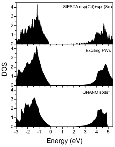
Figure 2 shows the bulk density of states (DOS) computed using three methods: the result of the density functional (DFT) LCAO calculation using the SIESTA packagesiesta_webpage (top panel), the plane-wave approach used in the package “Exciting”exciting_webpage (middle panel), and the DOS resulting from our TB approach (bottom panel). All three panels shows the DOS within the energy range of two gap energies into the valence and conduction bands, i.e., the range of energies of interest for the multiexciton generation process. Thus, our TB model gives results consistent with the two other, ab initio approaches up to eV into each of the conduction and valence bands.
The TB Hamiltonian in the above parametrization is used to compute the single-particle states in a spherical nanocrystal. The positions of all atoms in such a system are determined by cutting a spherical sample out of a bulk semiconductor, without any surface relaxation effects. The dangling bonds on the surface of the nanocrystal are passivated by the procedure involving the following steps: (i) rotation from the basis to that of hybridized orbitals, (ii) identification of the directions of resulting bonds and application of an energy shift of eV to those that are unsaturated, and (iii) inverse rotation into the basis.lee_oyafuso_prb03
II.2 Description of interacting electrons and holes confined in the nanocrystal
The excited states of the NC are expanded in electron and hole pair configurations. The electrons are defined as occupied states in the conduction band and holes as empty states in the valence band. With the operator () creating (annihilating) an electron on the single-particle state , while the operator () creating (annihilating) a hole on the single-particle state , the excited states are written as
| (3) |
where is the ground state of the NC. The amount of mixing among the configurations with different number of excitations is defined by the amplitudes , and depends on the energy of the state. The ground exciton state, whose energy is of order of the semiconductor gap , will be built predominantly out of single pair excitations, with a negligible contribution from the two-pair (energy at least of order of ) or higher configurations. On the other hand, the two-pair excitations may be mixed with highly excited single-pair configurations with similar energies. In this work we shall treat the number of quasi-particles as a good quantum number when labeling the states of the NC. A detailed analysis of the mixing effects will be presented elsewhere.
The Hamiltonian of interacting electrons and holes distributed on the single-particle states is
| (4) | |||||
In Eq. (4) the first two terms account for the single-particle energies, the third and fourth terms describe the electron-electron and hole-hole Coulomb interactions, respectively, and the last term introduces the electron-hole direct and exchange interactions. The Coulomb matrix elements are computed using the single-particle TB wave functions. In these computations we separate (i) the on-site terms arising from the scattered particles residing on the same atom, (ii) the nearest-neighbor (NN) terms involving orbitals localized on adjacent atoms, and (iii) the long-distance terms describing scattering between more remote atoms. Using the general form of our LCAO wave functions (1), each of these three elements can be written as follows:
| (5) | |||||
| (6) | |||||
| (7) | |||||
| (8) | |||||
and analogously for the hole-hole and electron-hole interactions. The necessary integrals in the on-site and nearest-neighbor terms are computed by approximating the atomistic functions by Slater orbitals.slater-pr1930 Note that in the above formulas we have assumed the two-center approximation. In an attempt to simulate the distance-dependent dielectric function,franceschetti_fu_prb99 ; wang_califano_prl03 ; moreels_allan_prb10 ; ogut_burdick_prl03 ; delerue_lannoo_prb03 each of these terms is scaled by a different dielectric constant . Typically we take and , the latter one being the bulk CdSe dielectric constant, while , i.e., half of the bulk CdSe value. In what follows we shall present two computations, one with the nearest neighbor term assuming the form identical to the remote term, and another one, with the nearest-neighbor term as in Eq. (7).
II.3 Calculation of optical spectra
Once the many-body states of the system of interacting electron-hole pairs are established, we calculate the emission spectra utilizing the Fermi’s Golden Rule
| (9) |
where is the energy of the initial state of excitons, is that of the final state of excitons, and the sum is carried over all possible final states. The temperature-dependent factor describes thermal population of levels of the initial exciton complex. The transition intensity is determined by the interband polarization operator, which for the polarization is defined as . The single particle dipole elements are defined as . The polarization operators for polarizations and are defined analogously. In our TB approach, the dipole matrix elements can be evaluated in the form:
| (10) | |||||
The integrals involving orbitals from the nearest and further neighbors are neglected. Absorption spectra are obtained using a formula analogous to Eq. (9), only the polarization operator is replaced by its Hermitian conjugate. In this case the initial state describes the system of excitons, with the appropriate thermal occupation of levels, while the final state contains electron-hole pairs.
III Single-particle states in the spherical nanocrystal
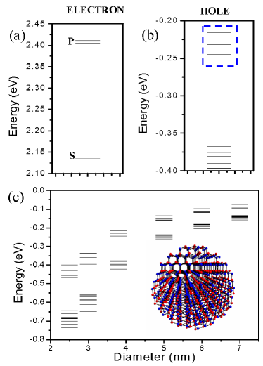
Figure 3 illustrates the single-particle properties of a spherical CdSe nanocrystal of diameter of nm, whose atomistic image is shown in the inset of Fig. 3(c). The system consists of atoms, with the Cd (Se) atoms rendered in blue (red). The energies of the single-particle electron and hole states obtained in the tight-binding calculation are shown in Figs. 3(a) and 3(b), respectively. The structure of electron states is typical for a spherical quantum confinement: the ground state of the symmetry is separated by a large gap (about meV) from three states of the symmetry. For the valence holes, however, we find four closely lying states, highlighted in Fig. 3(b) by the blue rectangle, separated from the remainder of the spectrum by a gap of about meV. This structure of the hole states is due to the interplay of the spin-orbit interaction and the crystal field splitting. The characteristic gap is robust and appears also for NCs with larger diameters, as illustrated in Fig. 3(c). The existence of four closely-lying hole states appears to be in agreement with results of earlier empirical pseudopotential calculations.franceschetti_fu_prb99 ; sewall_franceschetti_prb09
In the case of electron states, whose energies are shown in Fig. 3(a), the shell consists of three levels: almost degenerate and states at a higher energy, and a single non-degenerate level at a slightly lower energy. This is a signature of the wurtzite symmetry of the NC, which differentiates between the and directions, leading to a corresponding asymmetry in the electron wave function.
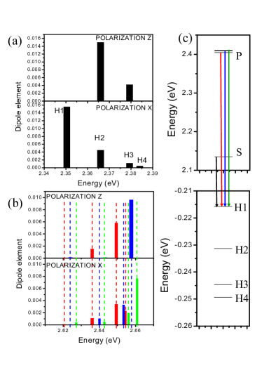
Insight into the symmetry of the four hole states emphasized in Fig. 3(b) can be gained by computing the dipole matrix elements built out of the -th electron and -th hole states, with and matrix elements constructed analogously. In Fig. 4(a) we plot the joint optical density of states (JDOS), i.e., magnitude of dipole elements versus the energy gap between the ground electron () and the four lowest hole states. For polarizations and we obtain four nonzero elements, while for polarization the JDOS consists of only two peaks. This structure of JDOS can be understood by approximating the atomistic wave functions as products of the envelope and Bloch part, as is done in the model. Since the envelope function changes slowly on interatomic distances, one typically approximates the dipole element by a product of the overlap of electron and hole envelope functions and an integral involving the Bloch components and the position operator appropriate for the , , or polarization. The electron ground state is built out of -type atomistic orbitals modulated by an -type envelope, while the hole states are built out of -type atomistic orbitals. Due to the spin-orbit mixing the envelope functions of the hole are mixtures of different symmetries.rego_hawrylak_prb97 However, this projectional analysis will extract the part of the envelope function of the hole which is of the same symmetry as the electron envelope function (in this case, symmetry ).
Using this approximation let us first analyze the lowest (H1) and highest (H4) JDOS maxima. They are present in the and polarizations, but absent in the polarization. This means that the -like term in the hole envelope function is associated with the Bloch functions consisting of and , but not atomic orbitals. The overlap of the electron and hole envelope functions is large for H1, but very small for H4, which indicates that the -like component dominates in the envelope function of the hole ground state, while the state H4 is of a different symmetry. The two middle JDOS peaks, H2 and H3, appear in all polarizations, indicating that the Bloch components of the corresponding hole functions are combinations of all three atomistic orbitals. Of those two, H2 is consistently stronger than H3, which suggests that the hole state H2 has a larger, and H3 - a smaller -like component.
Further confirmation of this assignment of symmetries is obtained by computing the dipole matrix elements between the electron states and the four hole states. This procedure probes the -like component in the hole envelope functions. The elements are shown in Fig. 4(b) as red, blue, and green bars, with the assignment of colors explained in Fig. 4(c). We find that the ground state H1 gives a negligible dipole matrix element with either of the three electron states, which confirms that the state H1 is of the type. On the other hand, the state H4 presents large dipole elements, which indicates that it has a dominating -like component in its envelope function.
As previously with the -type electron state, the two middle peaks, H2 and H3, appear consistently in both polarizations, but now H3 is larger. We conclude that the hole states H2 and H3 are mixtures of and -type envelopes. This assignment of symmetries is only approximate, as the details of the underlying crystal lattice and surface roughness break the rotational symmetry of the nanocrystal. However, a visual inspection of charge densities of the hole states suggests a picture consistent with the above analysis.
Note that all single-particle states are Kramers doublets, whose degeneracy is due to the time-reversal symmetry of the single-particle Hamiltonian. In what follows we shall distinguish the states forming the doublet by arrows up and down, respectively. Due to the spin-orbit interaction these labels cannot be identified with particle spins, but rather with Bloch total angular momenta.
IV Excitonic complexes in the nanocrystal
IV.1 Exciton
In order to find the energies and states of the exciton (X) we generate all possible electron-hole configurations in the single-particle basis, write the full Hamiltonian (4) in a matrix form in the basis of these configurations, and diagonalize this matrix numerically. Construction of the Hamiltonian requires knowledge of the Coulomb electron-hole scattering matrix elements. Typically one distinguishes two types of Coulomb matrix elements: the “direct” and the “exchange” ones, the latter originating from the antisymmetric character of the many-body wave function. This distinction is particularly clear in the case of diagonal matrix elements, i.e., those arising when one computes the expectation value of the Coulomb operator against any configuration. In this case the direct terms can involve pairs of particles with different spin, while the exchange elements connect particles with the same spins. Due to the spin-orbit interaction present in our TB model the single-particle states cannot be characterized by a definite spin. Moreover, as already mentioned, all single-particle states are in reality Kramers doublets, and any linear combination of the two constituent states is also a good eigenstate of the TB Hamiltonian. In order to be able to separate and analyze the Coulomb elements, we perform a rotation of each pair of states forming the Kramers doublet so as to optimize the expectation value of the Pauli operator. With the states thus prepared we compute the Coulomb elements using the formulas (5).
Let us now comment on the magnitudes of various Coulomb matrix elements for our NC with diameter of nm. We will discuss these elements in two cases, depending on the treatment of the nearest-neighbor contributions: (i) the case when these contributions are computed exactly using Slater orbitals, as shown in formula (7), (ii) the case when they are expressed simply by the formula (8) as for remote centers. In each case we scale the nearest neighbor contribution by the dielectric constant of , i.e., half of the CdSe bulk value.
If we denote the states composing the lowest-energy electron doublet as and , and the analogous pair of hole states as and , we find the direct elements: meV in the case (i), and meV in the case (ii). These elements define the interaction energy of an electron-hole configuration and , respectively, where denotes quasi-particle vacuum. The “spin-flip” electron scattering, described, e.g., by an element , is not possible, as the value of this element is negligibly small. However, due to the much stronger spin mixing of the hole states resulting from the spin-orbit interaction one might expect that the transitions involving the hole spin flip should be possible. In fact, here the only elements of note are meV in the case (i), and meV in the case (ii).
The scattering among the hole states, with the electron staying on the same level and without hole spin flip, and is very small. However, the scattering onto the fourth hole Kramers doublet, , is much larger and its absolute value amounts to meV in the case (i) and meV in the case (ii). Such an element describes the Coulomb coupling between configurations and . Also, scattering with hole transfer between the second and third Kramers doublet is sizeable and amounts to about meV in the case (i) and meV in the case (ii). The energy scales set by these Coulomb elements are to be compared with the energy separation of the hole states, which ranges from about to about meV. Thus, the diagonal Coulomb electron-hole terms, i.e., those that do not lead to a change of the electron-hole configuration, are about times larger than the separation of the hole states. On the other hand, the scattering elements, describing the change of configuration, are approximately of the same order as this separation. Therefore at this point it is not clear whether the ground state of the X can be approximated by a single configuration or it is rather a correlated system, with the hole spread out among the four lowest Kramers doublets.
The second type of the Coulomb matrix elements in play is the electron-hole exchange. Let us specify the exchange elements involving the lowest Kramers doublets - one for the electron and one for the hole. As these elements are spin sensitive, let us first point out that the TB model allows us to compute only the states of electrons in the conduction and valence bands. In order to describe the optics of our system in the usual language of quasi-particles, we have to change the treatment of the valence band by renaming the missing valence electron “spin up” into the valence hole “spin down”. Having this in mind, and working for the moment in the language of electrons only, we find that the absolute value of the element meV, while meV in the case (i). In the case (ii) the absolute value of these elements is meV and meV, respectively. In the language of quasi-particles these diagonal exchange terms describe the interaction correction to the electron-hole pairs with opposite spin (the former two elements) and parallel spin (the latter two elements). Since the electron-hole exchange interaction enters the total Hamiltonian with the positive sign, the quasi-particle pairs with antiparallel spins (i.e., the optically active ones) will have higher energy than those with parallel spins. The remaining exchange terms within this manifold of states are offdiagonal, and their absolute values do not exceed eV. As a result, due to the electron-hole exchange we expect a fine structure of the X composed of two pairs of states, separated by a gap of several meV, and each pair nearly degenerate.
To conclude the discussion of the electron-hole Coulomb matrix elements, we comment on how these elements are impacted by the difference in treatments of nearest neighbors, i.e., the cases (i) and (ii). We find that the treatment (ii) gives consistently larger magnitudes of the elements, however the difference is only about 5% in the direct terms and about 20% in the smallest exchange terms. From the general formulas for Coulomb elements given by Eqs. (7) and (8) we see that the nearest-neighbor term scales as the number of atoms , while the remote term scales as . As a result, the change in treatment of nearest neighbors will be more visible in smaller nanocrystals. In what follows we will employ the simplified treatment (ii), as the resulting change of energies is small compared to other energy scales in the system, and the simplification of the treatment of nearest neighbors leads to a considerable speedup in calculations.
Let us now move on to constructing the correlated states of the interacting electron-hole pair. As was already mentioned, we accomplish this by diagonalizing the Hamiltonian (4) set up in the basis of electron-hole configurations. With atoms present in the system, and the TB basis of orbitals per atom, we can distribute our particles on single-particle states, out of which we have hole and electron states. As a result, there exist excitonic configurations. Since in this work we focus on the low-energy excitonic configurations only, instead of dealing with the full basis we shall build the electron-hole configurations out of single-particle states closest to the bandgap. The computational effort grows rapidly with the increase of the number of single-particle basis involved in the calculation. The most time- and resource-intensive part is the computation of Coulomb matrix elements, as each element involves operations, and for electron and hole states we require electron-electron elements, hole-hole elements, and electron-hole elements.
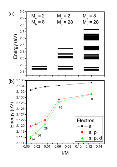
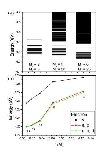
The evolution of the X spectra as a function of the basis size is visualized in Fig. 5(a). In the left-hand panel we show the X energies resulting from the diagonalization of the Hamiltonian built using electron states (i.e., the lowest, s-shell Kramers doublet) and hole states (i.e., the lowest four Kramers doublets separated from the rest of the hole spectrum by a gap). This results in electron-hole configurations. In the middle panel we include more hole states by increasing to , whilst in the right-hand panel we compute with (i.e., the s and p shells) and . This increase of the single-particle basis gives respectively and configurations. We see, overall, that as the basis is increased, the energy of the lowest level decreases, but not by a large amount compared to the bandwidth of the excitonic states. Moreover, the excitonic states are grouped into blocks separated by gaps. The lowest energy block, consistent throughout the three spectra, is built out of configurations from the lowest electronic doublet and the four lowest hole doublets of single-particle states. The second block, apparent in the middle panel, involves the hole residing on higher single-particle states, and the gap separating it from the lower section is consistent with the gap in the single-particle hole spectrum. Finally, in the right-hand panel we see two spectra from the middle panel, stacked on top of one another. Further, the top half of this ladder of states is denser than the bottom half. Such a distinct structure of the spectra is due to a large gap between the electron single-particle s and p shells. As a result, the third block from the bottom is composed of the hole residing on the four lowest single-particle levels, but the electron occupying one of the six p-shell levels. Similarly, the highest block contains configurations with an electron on the shell and the hole on states deeper in the valence band.
In Fig. 5(b) we show the dependence of the X ground-state energy on the hole basis size for three cases: electron on the shell only (black squares), on the and shells (red circles), and on the , , and shells (green triangles). We see that as a function of the X energy follows a power law and it is not completely converged even for the largest hole basis used ( states). We notice also a marked decrease of the X energy as subsequent electronic shells enter the picture. As the electron spreads to the p shell, the energy drops by about meV, while allowing the electron to spread to the d shell results in a smaller decrease. Note that the overall drop in energy is about meV, most of it accomplished by using the three electronic shells, , , and (altogether 18 states) and increasing the hole basis to states. The energy drop is of the order of Coulomb electron-hole direct scattering matrix elements and is somewhat larger than the separation of the lowest four hole single-particle states, but it is an order of magnitude smaller than the diagonal direct Coulomb elements describing the electron-hole attraction.
In view of the slow convergence of X energies it is necessary to establish a scheme for extraction of their converged values. To this end we first extrapolate each of the curves from Fig. 5(b) to zero (i.e., infinite number of hole basis states). Then we use the energies obtained for each to extrapolate to infinite number of electron states. In our case, the extrapolated ground-state energy of the exciton is eV.
Because of the commensurability of the energy change due to correlations and the single-particle energy scale we now examine the spectral content of the several low-lying X states in the case of and , i.e., in the regime when the energy is already relatively close to convergence. Figure 6(a) shows the lowest section of the energy spectrum of such an X, while panels (b) illustrate schematically the configurations dominant in the respective wave functions. We find that the two lowest X states are nearly degenerate (to within eV) and are composed predominantly (in 95%) of the configurations with the electron and hole occupying their respective lowest single-particle states, and , and assuming the same spin character (i.e., approximately “spin parallel”). Such configurations can be written as and and are shown schematically in the upper left-hand and upper right-hand panel of Fig. 6(b), respectively The next pair of states is found meV higher in energy, this gap being due predominantly to the electron-hole exchange. This pair is degenerate to within eV. The constituent states are composed of configurations, in which the electron and the hole have “opposite spins”. One of such configurations, is shown in the lower left-hand panel of Fig. 6(b). The other one, , is shown in the lower right-hand panel of that Figure.
IV.2 Bi-exciton
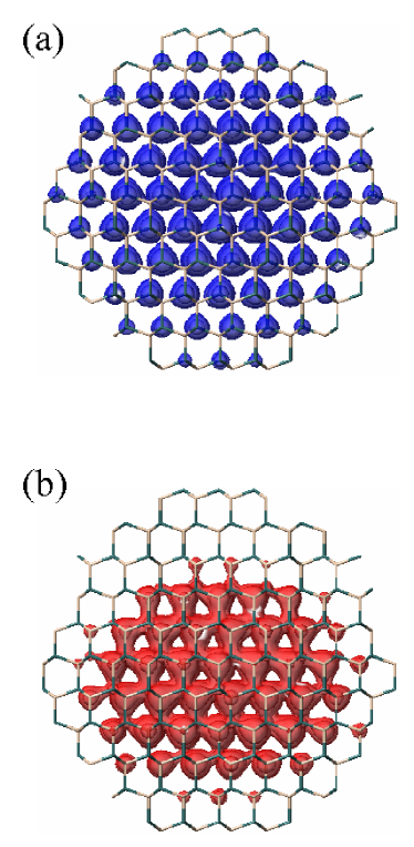
We now proceed to calculating the energies and wave functions of a system of two electron-hole pairs forming a bi-exciton (XX). Since now we deal with pairs of carriers of the same type, we need to establish the electron-electron and hole-hole matrix elements. In computations we also consider the two cases of treating the nearest-neighbor contributions, as discussed previously for the electron-hole elements. Let us consider the electron-electron elements first. The diagonal element defining the interaction energy of the two-electron configuration on the lowest single-particle levels is meV in the case (i) and meV in the case (ii). It is somewhat smaller (by about 5%) than the fundamental electron-hole element discussed in the previous Section. A similar element for the holes, defining the interaction energy of the hole pair is meV in the case (i) and meV in the case (ii). It is much larger than the fundamental electron-electron and electron-hole elements. We find this to be the case for all sizes of spherical CdSe nanocrystals studied (from nm to nm). A possible reason for this disparity between various types of matrix elements lies in the difference of charge densities corresponding to the electron and hole single-particle ground states. Figure 7(a) shows the vertical cross-section of the ground-state charge density for the electron computed by the QNANO package. As can be seen, this density is distributed across the entire crystal, it is largest in the center and tapers off towards the surfaces. Small irregularities in this image are due to the lack of the symmetry plane of the nanocrystal, which is built out of layers of atoms. This is why we find a finite density on the lowest atomic layer, while the top layer appears to carry no charge. An analogous profile for the ground hole state is shown in Fig. 7(b). Here we see a clear lack of symmetry, with the maximum charge located in the lower half of the nanocrystal. Also, the hole appears to occupy a much smaller volume than the electron does. Note that neither of the wave functions is centered in the NC. This is due to wurtzite structure of NC, particularly due to polarity of the (0001) direction which results in the development of internal dipole moment. We have confirmed the existence of such a dipole in our DFT calculations (not shown here), however we find that the direction and strength of this dipole is sensitive to the type of ligands used to passivate the NC surface. The decreased spatial extent of the hole state leads to a large magnitude of the Coulomb repulsion of two holes placed on the lowest Kramers doublet, since the charge density of these two states is identical. In the electron case the more uniform spread of the density across the crystal diminishes the electron-electron element. The electron-hole element is also decreased, as we deal here with a relatively localized hole interacting with a distributed electron charge.
Let us now look at the scattering matrix elements, which describe the Coulomb coupling between different configurations. For holes the largest element transferring the particle from the lowest Kramers doublet is meV in the case (i) and meV in the case (ii). To assess the strength of this element in a meaningful way, let us first analyze briefly a two-hole configuration . Compared to the fundamental configuration , the excited configuration is created by moving the hole from the first to the fourth Kramers doublet and so its single-particle energy is higher by about meV. On the other hand, the interaction energy of the excited two-hole configuration is given by the matrix element , which is meV in the case (i) and meV in the case (ii). That is, in this excited configuration the holes repel by about meV weaker than in the fundamental one. So, altogether, the configuration is lower in energy, even though it has a larger single-particle energy part. The energy difference between the two configurations is then only about meV, suggesting that the offdiagonal scattering matrix elements will lead to the appearance of strongly correlated hole-hole states.
Let us now account for the presence of the two electrons. The electron-hole attraction gives a negative contribution to the total energy of the system. In any XX configuration we have four constituent terms, as each electron attracts two holes. For this discussion we need also the electron-hole matrix element meV in case (i) and meV in case (ii). Comparing this element with the fundamental electron-hole direct element given in the previous section we see that the electron attracts the hole on the level by about meV weaker than it does the hole on the ground single-particle level. Now we are in a position to compare the energies of configurations and . Owing to the electron-hole direct terms we find that the former, i.e., the fundamental configuration of the two electron-hole pairs, is about meV lower in total energy than that with one excited hole. As we see, the final alignment of levels results from cancellations of large interaction terms of comparable magnitude, and as such will be sensitive to the details of many-body computation.
The smallest contribution to scattering comes from the electron-electron interaction. Transfer of one electron from the -shell orbitals to the -shell orbitals due to this interaction is described, e.g., by an element meV in the case (i) and meV in the case (ii). This is to be compared with the energy gap between the and electronic shells, which amounts to meV. So, the spread of electrons onto the shell due to the electron-electron interaction is expected to be small.
We now proceed to diagonalizing the two-pair Hamiltonian as a function of the size of the single-particle basis. Figure 8(a) shows the energy levels of the system with , (left), , (middle), and , (right). In the first case we populate only the lowest electronic Kramers doublet and the four lowest hole Kramers doublets. As a result we can create configurations. The left-hand panel of Fig. 8(a) shows all resulting XX eigenenergies. As we increase the hole basis, and later on also the electron basis, we allow one or both particles of each type to populate higher-energy single-particle states. This results in a buildup of the density of XX states at higher energies, which is clearly visible in the middle and right-hand panels of Fig. 8(a). Also, the low-lying XX energy states appear to shift down in energy by tens of meV. To analyze this shift in greater detail, in Fig. 8(b) we plot the energies of the XX states with dominant singlet-singlet configuration as a function of the size of the hole basis in three cases: with both electrons on the state (black squares), with the electrons allowed to spread onto the shell (red circles) and with the electrons populating the , , and shells (green triangles). Note that the state under consideration is not always the ground state of the system, which reflects the simple analysis outlined above. This state stabilizes as the ground state for hole basis of at least states, while for smaller excitation of one of the holes is preferred.
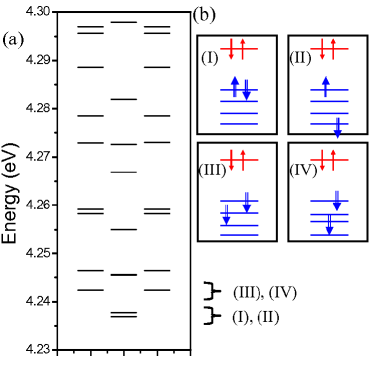
As we can see, the energy decreases steadily if we increase the hole basis size but keep a constant number of electron states. On the other hand, for a constant hole basis one large drop takes place as we increase the electron basis from to states. Upon its further increase to states the energy change is much less significant. A systematic study of the convergence of ground state energy is much more difficult here, as for the basis , we already deal with two-pair configurations. Using the procedure analogous to that described in the previous Section, we extrapolate the ground-state XX energy to the limit of infinite basis and obtain eV. Figure 8(a) shows that in spite of the substantial energy change of the ground state, the block of lowest states appears to be separated from the remaining spectra, suggesting that the configurations with lowest single-particle energy contribute to their respective eigenvectors the most. To demonstrate this, in Fig. 9 we analyze the spectral content of several lowest eigenstates of the system with , . Figure 9(a) shows the lowest energy levels, consistent with the number of possible configurations created out of lowest electron and hole single particle blocks. As we can see, the lowest states are found just within a meV window, i.e., a fraction of the value of the fundamental Coulomb matrix elements. This is the central result of this work. We find that in the case of spherical CdSe nanocrystals the peculiar arrangement of hole single-particle levels together with Coulomb interactions lead to the appearance of a fine structure of bi-exciton levels.
In Fig. 9(b) we show configurations dominant in the lowest four XX states. The first two states, denoted respectively as (I) and (II), correspond to the two configurations analyzed before and behave as we predicted previously using the single-configuration arguments. The configuration predominant in the ground state is the “singlet-singlet” one, shown in panel (I), and created by placing the pairs of carriers on lowest possible single-particle levels. The first excited state, on the other hand, is based on the configuration where the hole is excited to the fourth Kramers doublet, shown in the panel (II). Note that the gap between these two states, amounting to about meV, is of the order of the electron-hole exchange energy, but it originates from correlations rather than exchange. The first excited state also contains significant admixtures of configurations, in which the holes occupy the two middle Kramers doublets in the low-energy section (not shown). At even higher energy we find a pair of nearly degenerate states, in which the holes have aligned “spins”. The dominant configurations in these states are shown in panels (III) and (IV), respectively.
IV.3 Optical spectra of exciton and bi-exciton
Having described the electronic properties of the X and XX confined in the NC we now proceed to discussing their optical spectra. We will conduct our analysis for the systems built upon electron and hole single-particle states. We start with the absorption spectrum of the exciton, shown in Fig. 10 and focus on the lowest spectral lines of that spectrum, i.e., those corresponding to the electron on the shell and the hole on one of the four lowest Kramers doublets. We find that the two lowest, nearly degenerate states of the exciton are optically dark irrespective of polarization, while the second pair of states is bright, but only in polarizations and . The two pairs of states form the fine structure of the exciton, in which the energy gaps are due to the electron-hole exchange. In these two polarizations we also find a third, even larger maximum at a slightly higher energy. Analysis of the spectral content of the corresponding X eigenstate reveals that it consists of a mixture of configurations in which the hole resides on the second and third Kramers doublet, with a smaller admixture of the fundamental configurations shown in Fig. 6(b)(II). Each of these configurations contributes constructively to the large final absorption amplitude of this state. The spectrum in polarization is different: it consists only of one large maximum, larger than any of the maxima in polarizations and . This large amplitude comes from the predominant distribution of the hole on the second single-particle Kramers doublet, which introduces a large oscillator strength in the polarization, as evident from Fig. 4(a). The general properties of the exciton spectrum, the multiplicities of the states and their oscillator strength obtained in our calculation agree well with previous empirical pseudopotential,franceschetti_fu_prb99 tight-bindingleung_pokrant_prb98 and qualitative calculations.efros_rosen_prb96
The absorption spectrum discussed above is equivalent to the emission spectrum of the X at high temperature, i.e., when the occupations of all X energy levels are similar. However, at low temperature only the lowest states will be occupied, and the emission spectrum will consist predominantly of the lowest line of the exciton. As this exciton state is dark, its radiative lifetime is expected to be very long. This suggests that owing to the characteristic alignment of the hole single-particle levels the X emission spectrum will sensitively depend on the temperature, with the dominant maxima appearing at higher energy as the temperature is increased.
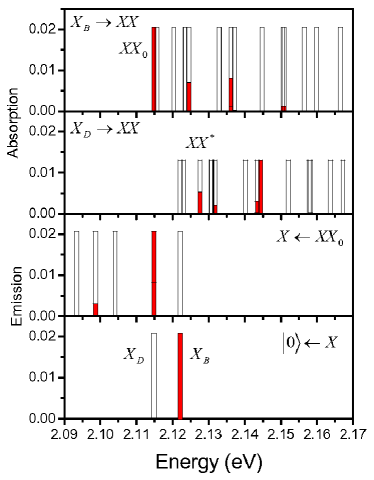
Let us move on to computing the optical spectra of the XX. Figure 11 shows its absorption (two top panels) and emission spectra (third panel from the top). Calculation of the absorption spectrum involves preparing the single exciton system in the bright, second excited state (top panel) or dark, ground state (second panel from the top) and adding the second electron-hole pair to form the ground and excited XX states. Due to the optical selection rules, the carriers composing the photo-created electron-hole pair must have antiparallel spins.
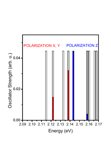
Let us first discuss the absorption spectra involving an addition of the second electron-hole pair to the bright exciton. We find that this spectrum is composed of several peaks, one at energy eV, and denoted as , the second one at energy about eV, and the third one at energy about eV. The low-energy peak corresponds to addition of an optically active electron-hole pair to the bright exciton configuration as in Fig. 6(b)(I) and formation of the ground state bi-exciton as in Fig. 9(b)(I). The two higher-energy peaks correspond to the formation of an excited bi-exciton, in which the holes are redistributed among the four lowest Kramers doublets, however retaining their “spin unpolarized” character.
If the exciton is prepared in the ground, dark state, the XX absorption spectrum (Fig. 11, second panel from the top) is dominated by two groups of peaks, one around the energy of about eV, denoted as , and the second at energy eV, indicating the formation of excited XX states. This is because at any lower energy the optical selection rules prevent us from adding a photoexcited, spin-unpolarized electron-hole pair to the spin-parallel ground X state. The resulting XX states contain spin-polarized holes.
In the calculation of the emission spectrum (third panel of Fig. 11) we prepare the XX in its ground, singlet-singlet state. We find that the emission spectrum is dominated by one maximum, corresponding to the bright exciton final state [(II) in Fig. 6(b)]. It is accompanied by a small maximum at lower energy. Note that the main maximum is found at the same energy as the low-energy absorption peak of the bright exciton (top panel). However, there is an energy gap between the emission and dark exciton absorption peaks, due to the fine structure of both the exciton and bi-exciton low-energy spectra.
Finally, the bottom panel of Fig. 11 shows the emission spectra of the exciton. The low-energy peak corresponds to the dark, ground state , whilst the high-energy peak denotes the radiative transition from the bright, excited state of the exciton.
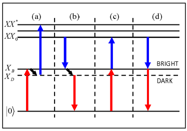
Since in our calculations we have not accounted for the dynamics of carriers, and in particular the relaxation processes, the above emission and absorption spectra should be understood as presentation of oscillator strengths for various transitions rather than candidates for direct comparisons with experimental data. To make this point clear, in Fig. 12 we present two possible absorptive and emissive scenarios in our system. In Figure 12(a) and (b) we assume that the relaxation from the excited, bright state to the ground, dark state is faster than the radiative recombination from either of these two states. Panel (a) shows the absorption from the vacuum to the XX state. We start with the optical creation of an exciton in its bright state (the red arrow), followed by its relaxation to the dark state (the black arrow). According to Fig. 10, the absorption process should take place at the energy of about eV. We can now create the XX, but only in one of its excited states, such as the one denoted as in Fig. 11 (second panel from the top). This absorption event should be observable at the energy of about eV, i.e., we predict the XX binding energy in this absorptive process to be negative.
The emissive cascade under the assumption of fast relaxation is shown in Fig. 12 (b). We start with XX in its ground state , recombining radiatively and leaving the system with the X in its excited, bright state . According to Fig. 11 (third panel from the top), this process is seen in the emission as a maximum at eV. The exciton further relaxes to the dark state and may recombine with a very long lifetime. The recombination energy appears to be also eV, but its degeneracy with the XX emission energy is here accidental and cannot be treated as the universal property of the NCs. To summarize, assuming the fast X relaxation we find the absorptive XX binding energy to be meV, while the emissive binding energy is zero.
Let us now consider the situation in which the X relaxation from its bright to dark state is the slowest process. The absorption processes under this condition are visualized in Fig. 12 (c). Here we create the X in its bright state at the energy eV, and then immediately afterwards the XX in its ground state . According to Fig. 11 (top panel), the latter transition should be seen as an absorption maximum at eV, producing the absorptive XX binding energy of meV. The emissive cascade under the same condition is shown schematically in Fig. 12 (d). As the cascade utilizes the same X and XX states as the absorptive process, we expect the XX emissive binding energy in our system to be also equal to meV.
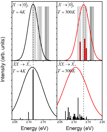
Let us now present a detailed comparison of the XX and X emission spectra. As already mentioned, the exciton recombines to vacuum, and therefore the position of the respective emission peak equals to the energy of the X. In the simplest treatment we approximate the X state by one configuration . The emission energy of such a state, neglecting for now the electron-hole exchange, is . The bi-exciton, on the other hand, recombines to the final-state exciton. The energy of the fundamental XX configuration is and accounts for the repulsion of the like carriers and attraction of each pair of opposite carriers. The position of the XX fundamental emission peak can then be evaluated as . It consists of the exciton energy and self-energy corrections. If the electron-electron and hole-hole elements are equal to the electron-hole terms, the self-energy corrections cancel out and the XX emission peak matches that of the exciton. However, as demonstrated above, the hole-hole repulsive interaction is significantly larger than the electron-hole element, and so from that simple analysis we expect the XX peak to occur at the energy higher than that of X, i.e., we expect the XX to be unbound, as is found in some epitaxial dots (see e.g. Ref. reimer_dalacu_jpcs2010, ).
Let us now compare the emission peak positions of X and XX.achermann_hollingsworth_prb03 ; klimov_ivanov_nature07 Figure 13 shows these spectra on the same energy scale. The bars in the two top panels show the complete X emission spectrum assuming equal occupation of all levels (infinite temperature), while the black and red curves account for finite temperature effects. At the temperature of K (top left panel) only the ground state of the exciton will be occupied, as it is separated from the excited states by the electron-hole exchange gap. As a result, the low-temperature X recombination is forbidden optically, resulting in a long excitonic lifetime. Assuming long integration time, and accounting for a model inhomogeneous broadening, such a recombination maximum is schematically shown in Fig. 13(top left panel) with a black line. Note that in this graph only the position of this peak is meaningful, since, as we have already mentioned, we do not model dynamical phenomena taking place in the system. On the other hand, as the temperature is increased to K, excited X states are populated, resulting in optically allowed excitonic recombination.
The high-temperature emission maximum computed assuming the Maxwell-Boltzmann thermal distribution of carriers and including model inhomogeneous broadening, is shown with the red continuous line in the top right panel of Fig. 13. As already discussed, this maximum is shifted towards higher energies by about meV.
Let us now move on to the XX spectra (the two bottom panels of Fig. 13). Since the XX ground state is optically active, we deal with relatively short XX lifetimes even at very low temperatures. Such a low-temperature spectrum is plotted in Fig. 13(lower left panel) with black bars, while the black continuous line is the emission envelope accounting for a model inhomogeneous broadening. As the temperature is increased, excited XX states will become populated. This, however, does not have to mean that the emission peak will shift towards higher energies, as was the case for the exciton. Indeed, the XX states recombine to excited X states, while the X states can only recombine to the vacuum. Depending on the oscillator strengths appropriate for each of the possible XX-X transitions we may deal with additional higher-energy peaks (when excited XX states recombine to low-lying X states) or low-energy maxima (when the final X states lie high in energy). Figure 13(lower right panel) demonstrates that in the studied system we deal with the latter case. If we also account for inhomogeneous broadening (red continuous line), we find that the overall emission maximum moves towards lower energies, i.e., exhibits a trend opposite to that of the exciton.
Let us now compare the two spectra. In the K case (the two left panels), due to the interplay of Coulomb elements, we predict the XX emission peak at a slightly higher energy than the X maximum, i.e., we find that the XX becomes unbound. However, as the temperature is raised to K (the two right panels), the opposite shifts in the X and XX spectra lead to a rearrangement of the order of the peaks, so that the XX maximum is found below the X.
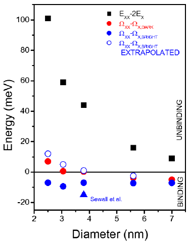
In the last element of our analysis we study the relative positions of the X and XX emission maxima as a function of the NC size. In Fig. 14 we show several characteristic quantities measuring the position of the XX peak relative to the X peak, i.e., the XX binding energy. Black squares show the difference computed earlier in the single-configuration approach neglecting the electron-hole exchange. As can be seen, this difference is positive (i.e., the XX is unboundefros_rodina_ssc89 ) for all NC sizes studied. Next we include the electron-hole exchange effects and correlations by computing the XX binding energy with the basis of and single-particle states. In this case we present two sets of results, shown with filled symbols. The red (blue) circles show the difference between the XX lowest-energy peak and that of the dark (bright) exciton; the splitting between these two sets of data is due to the electron-hole exchange. We find that if the position of the XX peak is measured relative to the dark exciton, the XX becomes unbound for NC diameters smaller than nm. On the other hand, if the bright exciton is considered, the XX is always bound, in contrast to the single-configuration calculation. However, as demonstrated earlier, the basis set taken in this calculation is not sufficient to achieve convergence of the X and XX energies. To eliminate this systematic error, we extrapolate the X and XX energies presented in Fig. 5 and 8, respectively, to the infinite hole basis. The XX binding energy computed in this limit relative to the bright X maximum is shown in Fig. 14 with empty symbols. We find that the XX is unbound for NC diameters smaller than nm, and bound for larger NC diameters. We compare our results to those obtained by Sewall et al. (Ref. sewall_franceschetti_prb09, ) in a finite electron and hole basis set. The XX binding energy obtained in this empirical pseudopotential calculation is denoted by the blue triangle for the NC diameter of nm. In agreement with our finite-basis calculation, Sewall et al. predict a bound XX. Note, however, that after extrapolation to the infinite basis set the XX becomes unbound, which demonstrates the need for systematic convergence study.
V Conclusions
In conclusion, we have analyzed the electronic and optical properties of an exciton and a bi-exciton confined in a single, spherical CdSe nanocrystal. Using the atomistic tight-binding approach we have calculated the single-particle spectra and found that the lowest energy hole states form a shell consisting of four states separated from the rest of levels by a gap. The bi-exciton state was computed using configuration interaction techniques and found to be a strongly correlated state consisting of a two electron singlet in the -shell of the conduction band and a strongly correlated state of two holes distributed on the degenerate hole shell, resulting in a fine structure of bi-exciton energy levels. The fine structure is also present in the exciton spectrum, however it is due to the electron-hole exchange interaction. The bi-exciton fine structure becomes apparent in the absorption of the second exciton into the nanocrystal. We find that if the initial state exciton is prepared in the bright configuration, the maximum indicating the absorption of the second pair is found at the same energy as the emission peak from XX. However, if we prepare the exciton in the dark state, the absorption takes place to higher XX states in the quasi-degenerate manifold. As for the emission spectra, we found that at a low temperature the bi-exciton emission peak corresponds to an energy slightly higher than the energy of the excitonic ground, dark state, i.e., the XX is unbound. However, at higher temperatures the exciton emits from the excited bright state, so that the inhomogeneously broadened X emission peak moves to higher energies. On the other hand, thermal population of higher XX levels leads to emission to excited final X states, moving the broadened XX emission peak to lower energies, even below the high-temperature emission maximum. A similar transition in the character of XX can be achieved by changing the diameter of the nanocrystal: for diameters of up to nm the XX is unbound, while for larger NCs the XX becomes bound. Due to the complicated nature of the spectrum of the valence hole we find that in all elements of our analysis the correlations play a crucial role and that any qualitative conclusions as to the electronic and optical properties of X and XX can be drawn only after a careful convergence analysis.
Future work will focus on improving several aspects of QNANO which at present received only a model treatment. We plan to improve the description of screening and carry out a computation of the distance-dependent dielectric function.wang_califano_prl03 ; franceschetti_fu_prb99 ; moreels_allan_prb10 ; ogut_burdick_prl03 ; delerue_lannoo_prb03 We are going to develop a more realistic model of the surface passivation accounting for the presence of ligands. The more microscopic description of the surface is also needed for a proper description of the NC shape. We plan to develop a hybrid tb-DFT QNANO package in order to account for a realistic surface reconstruction and faceting.
Acknowledgment
The authors acknowledge discussions with G. Scholes, Kui Yu, A. Stolow, P. Kambhampati, A. Efros, M. Zielinski, and thank E. Kadantsev for providing the results of DFT calculations with the EXCITING/elk software (Figs. 1, 2). Funding from the NRC-NSERC-BDC Nanotechnology Project and CIFAR is gratefully acknowledged.
References
- (1) V.I. Klimov, Annu. Rev. Phys. Chem. 58, 635 (2007).
- (2) G. Nair, S.M. Geyer, L.-Y. Chang, and M.G. Bawendi, Phys. Rev. B 78, 125325 (2008).
- (3) I.Gur, N.A. Fromer, M.L. Geier, and A.P. Alivisatos, Science 310, 462 (2005).
- (4) M. Nirmal, B.O. Dabbousi, M.G. Bawendi, J.J. Macklin, J.K. Trautman, T.D. Harris, and L.E. Brus, Nature 383, 802 (1996).
- (5) L.E. Brus, Nano Lett. 10, 363 (2010).
- (6) A.I. Ekimov, F. Hache, M.C. Schanne-Klein, D. Ricard, C. Flytzanis, I.A. Kudryavtsev, T.V. Yazeva, A.V. Rodina, and Al.L. Efros, J. Opt. Soc. Am. B 10, 100 (1993).
- (7) R.J. Ellingson, M.C. Beard, J.C. Johnson, P. Yu, O.I. Micic, A.J. Nozik, A. Shabaev, and A.L. Efros, Nano Lett. 5, 865 (2005).
- (8) G. Scholes, Adv. Funct. Mater. 18, 115 (2008).
- (9) G. Scholes and G. Rumbles, Nature Materials 5, 683 (2006).
- (10) D. Yu, C. Wang, and P. Guyot-Sionnest, Science 300, 1277 (2003).
- (11) A. Pandey and P. Guyot-Sionnest J. Chem. Phys. 127, 111104 (2007)
- (12) D.E. Gomez, M. Califano, and P. Mulvaney, Phys. Chem. Chem. Phys. 8, 4989 (2006).
- (13) See e.g. Y. Yin and A.P. Alivisatos, Nature 437, 664 (2005), and references therein.
- (14) A.H. Fu, W.W. Gu, C. Larabell, and A.P. Alivisatos, Current Opinion in Neurobiology 15, 568 (2005).
- (15) A.P. Alivisatos, Nature Biotechnology 22, 47 (2004).
- (16) W.C.W. Chan and S.M. Nie, Science 281, 2016 (1998).
- (17) V.L. Colvin, M.C. Schlamp, and A.P. Alivisatos, Nature 370, 354 (1994).
- (18) B.O. Dabbousi, M.G. Bawendi, O. Onitsuka, and M.F. Rubner, Appl. Phys. Lett. 66, 1316 (1995).
- (19) S. Chanyawadee, P.G. Lagoudakis, R.T. Harley, M.D.B. Chariton, D.V. Talapin, H.W. Huang, and C.-H. Lin, Advanced Materials 22, 602 (2009).
- (20) G. Konstantatos and E.H. Sargent, Nature Nanotechnology doi:10.1038/nnano.2010.78
- (21) V. Sukhovatkin, S. Hinds, L. Brzozowski, and E.H. Sargent, Science 324, 1542 (2009).
- (22) A.G. Pattantyus-Abraham, H. Qiao, J. Shan, K.A. Abel, T.-S. Wang, F.C.J.M. van Veggel, and J.F. Young, Nano Lett. 9, 2849 (2009).
- (23) V.I. Klimov, A.A. Mikhaelovsky, S. Xu, A. Mlko, and J.A. Hollingsworth, Science 290, 314 (2000).
- (24) C. Weisbuch, J. Cryst. Growth 138, 776 (1994).
- (25) V.I. Klimov, S.A. Ivanov, J. Nanda, M. Achermann, I. Bezel, J.A. McGuire, and A. Piryatinsky, Nature 447, 441 (2007).
- (26) R.R Cooney, S.L. Sewall, D.M. Sagar, and P. Kambhampati, Phys. Rev. Lett. 102, 127404 (2009).
- (27) H.W. Hillhouse and M.C. Beard, Current Opnion in Colloid and Interface Science 14, 245 (2009).
- (28) C. Wadia, A.P. Alivisatos, and D.M. Kammen, Environ. Sci. Technol. 43, 2072 (2009).
- (29) J.M. Luther, M. Law, M.C. Beard, Q. Song, M.O. Reese, R.J. Ellingson, and A.J. Nozik, Nano Lett. 8, 3488 (2009).
- (30) J.J. Choi, Y. Lim, M.B. Santiago-Berrios, M. Oh, B. Hyun, L. Sun, A.C. Bartnik, A. Goedhart, G.G. Malliaras, H.D. Abruna, F.W. Wise, and T. Hanrath, Nano Lett. 9, 3479 (2009).
- (31) K.W. Johnston, A.G. Pattantyus-Abraham, J.P. Clifford, S.H. Myrskog, D.D. McNeil, L. Levina, and E.H. Sargent, Appl. Phys. Lett. 92, 151115 (2008).
- (32) A.J. Nozik, Physica E 14, 115 (2002).
- (33) E. Rabani and R. Baer, Nano Lett. 8, 4488 (2008).
- (34) R.D. Schaller, J.M. Pietryga, and V.I. Klimov, Nano Lett. 7, 3469 (2007).
- (35) A. Franceschetti, J.M. An, and A. Zunger, Nano Lett. 6, 2191 (2006).
- (36) G. Nair and M.G. Bawendi, Phys. Rev. B 76, 081304 (2007).
- (37) A.J. Nozik, Annu. Rev. Phys. Chem. 52, 193 (2001).
- (38) R.D. Schaller and V.I. Klimov, Phys. Rev. Lett. 92, 186601 (2004).
- (39) A.J. Nozik, Chem. Phys. Lett. 457, 3 (2008).
- (40) R.D. Schaler, M. Sykora, J.M. Pietryga, and V.I. Klimov, Nano Lett. 6, 424 (2006).
- (41) J.A. McGuire, M. Sykora, J. Joo, J.M. Pietryga, and V.I. Klimov, Nano Lett. 10, 2049 (2010).
- (42) A. Shabaev, Al.L. Efros, and A.J. Nozik, Nano Lett. 6, 2856 (2006).
- (43) J.A. McGuire, J. Joo, J.M. Pietryga, R.D. Schaller, and V.I. Klimov, Acct. Chem. Research 41, 1810 (2008).
- (44) R.D. Schaller, V.M. Agranovich, and V.I. Klimov, Nature Phys. 1, 189 (2005).
- (45) L. Silvestri and V.M. Agranovich, Phys. Rev. B 81, 205302 (2010).
- (46) Al.L. Efros, M. Rosen, M. Kuno, M. Nirmal, D.J. Norris, and M. Bawendi, Phys. Rev. B 54, 4843 (1996).
- (47) K. Leung, S. Pokrant, and K.B. Whaley, Phys. Rev. B 57, 12291 (1998).
- (48) P. Chen and K.B. Whaley, Phys. Rev. B 70, 045311 (2004).
- (49) S. Sapra and D.D. Sarma, Phys. Rev. B 69, 125304 (2004).
- (50) C. Delerue, G. Allan, and Y.M. Niquet, Phys. Rev. B 72, 195316 (2004).
- (51) L.W. Wang and A. Zunger, J. Phys. Chem. B 102, 6449 (1998).
- (52) A. Franceschetti, H. Fu, L. Wang, and A. Zunger, Phys. Rev. B 60, 1819 (1999).
- (53) M. Califano, A. Franceschetti, and A. Zunger, Phys. Rev. B 75, 115401 (2007).
- (54) S.L. Sewall, A. Franceschetti, R.R. Cooney, A. Zunger, and P. Kambhampati, Phys. Rev. B 80, 081310 (2009).
- (55) M. Achermann, J.A. Hollingsworth, and V.I. Klimov, Phys. Rev. B 68, 245302 (2003).
- (56) J.-M. Caruge, Y. Chan, V. Sundar, H.J. Eisler, and M.G. Bawendi, Phys. Rev. B 70, 085316(2004).
- (57) C. Bonati, M.B. Mohamed, D. Tonti, G. Zgrablic, S. Haacke, F. van Mourik, and M. Chergui, Phys. Rev. B 71, 205317 (2005).
- (58) R. Osovsky, D. Cheskis, V. Kloper, A. Sashchiuk, M. Kroner, and E. Lifshitz, Phys. Rev. Lett. 102, 197401 (2009).
- (59) H. Htoon, S.A. Crooker, M. Furis, S. Jeong, Al.L. Efros, and V.I. Klimov, Phys. Rev. Lett. 102, 017402 (2009).
- (60) M. Furis, H. Htoon, M.A. Petruska, V.I. Klimov, T. Brrick, and S.A. Crooker, Phys. Rev. B 73, 241313(R) (2006).
- (61) Single Quantum dots: Fundamentals, Applications, and New Concepts, edited by Michler, P., Topics in Applied Physics, Vol. 90 (Springer-Verlag, Berlin, 2003).
- (62) S.L. Sewall, R.R. Cooney, K.E.H. Anderson, E.A. Dias, and P. Kambhampati, Phys. Rev. B 74, 235328 (2006).
- (63) S.L. Sewall, R.R. Cooney, K.E.H. Anderson, E.A. Dias, D.M. Sagar, and P. Kambhampati, J. Chem. Phys. 129, 084701 (2008).
- (64) J. Shumway, A. Franceschetti, and A. Zunger, Phys. Rev. B 63, 155316 (2001
- (65) M. Korkusinski, M. Zielinski, and P. Hawrylak, J. Appl. Phys. 105, 122406 (2009).
- (66) Landolt-Bornstein Numerical Data and Functional Relationships in Science and Technology, edited by O. Madelung, Springer, Berlin, 1987.
- (67) S. Sapra, N. Shanthi, and D.D Sarma, Phys. Rev. B 66, 205202 (2002).
- (68) R. Visvanatha, S. Sapra, T. Saha-Dasgupta, and D.D. Sarma, Phys. Rev. B 72, 045333 (2005).
- (69) H. Hakan Gürel, Ö. Akincki, and H. Ünlü, Thin Solid Films 516, 7098 (2008).
- (70) O. Zakharov, A. Rubio, X. Blase, M.L. Cohen, and S.G. Louie, Phys. Rev. B 50, 10780 (1994).
- (71) http://elk.sourceforge.net
- (72) http://www.icmab.es/siesta
- (73) S. Lee, F. Oyafuso, P. von Allmen, and G. Klimeck, Phys. Rev. B 69, 045316 (2003).
- (74) J. C. Slater, Phys. Rev. 36, 57 (1930).
- (75) L.W. Wang, M. Califano, A. Zunger, and A. Franceschetti, Phys. Rev. Lett. 91, 056404 (2003).
- (76) I. Moreels, G. Allan, B. De Geyter, L. Wirtz, C. Delerue, and Z. Hens, Phys. Rev. B 81, 235319 (2010).
- (77) S. Ogut, R. Burdick, Y. Saad, and J.R. Chelikovsky, Phys. Rev. Lett. 90, 127401 (2003).
- (78) C. Delerue, M. Lannoo, and G. Allan, Phys. Rev. B 68, 115411 (2003).
- (79) L.G.C. Rego, P. Hawrylak, J.A. Brum, and A. Wojs, Phys. Rev. B 55, 15694 (1997).
- (80) Al.L. Efros and A.V. Rodina, Solid State Comm. 72, 645 (1989).
- (81) M.E. Reimer, D. Dalacu, P.J. Poole, and R.L. Williams, J. Phys.: Conference Series 210, 012019 (2010).