Electronic structure of BaNi2As2
Abstract
BaNi2As2, with a first order phase transition around 131 K, is studied by the angle-resolved photoemission spectroscopy. The measured electronic structure is compared to the local density approximation calculations, revealing similar large electronlike bands around and differences along -. We further show that the electronic structure of BaNi2As2 is distinct from that of the sibling iron pnictides. Particularly, there is no signature of band folding, indicating no collinear SDW related magnetic ordering. Moreover, across the strong first order phase transition, the band shift exhibits a hysteresis, which is directly related to the significant lattice distortion in BaNi2As2.
I Introduction
The discovery of iron-based high-temperature superconductors has ignited intensive studies.Kamihara ; Chen_Sm1 ; ZARen_Sm ; Chen_Sm2 ; MXu ; CLWang_Sm ; ZARen_Nd ; Kursumovic_Nd ; ZARen_Pr The superconducting transition temperature () has risen up to 56 K in FeAsO1-xFx (=Sm, Nd, Pr, …).ZARen_Sm ; Chen_Sm2 ; CLWang_Sm ; ZARen_Nd ; Kursumovic_Nd ; ZARen_Pr On the other hand, the sibling Ni-based compounds only possess relatively low , i.e., LaONiP (=3 K),LaONiP LaONiAs (=2.75 K),LaONiAs BaNi2P2 (=2.4 K),BaNi2P2 BaNi2As2 (=0.7 K),Ronning and SrNi2As2 (=0.62 K).SrNi2As2 . It is intriguing to understand why is low in the Ni-based compounds, which may facilitate understanding the high- in iron-based ones.
BaFe2As2, a typical parent compound of iron-based superconductor with the ThCr2Si2 structure, exhibits a structural transition from tetragonal to orthorhombic, concomitant with a spin-density-wave (SDW) transition at 140 K.Rotter The structural transition was suggested to be driven by the magnetic degree of freedom.Yildirim ; CFang ; Cenke ; CHe ; LX1111 ; NLWang_1111 BaNi2As2 with the same structure, displays a structural transition around 131 K, however, from a tetragonal phase to a lower symmetry triclinic phase.Sefat No evidence of SDW is reported in BaNi2As2 so far. On the other hand, it was pointed out that the transition in BaNi2As2 is a first-order one, while that is more second-order-like in BaFe2As2.Sefat Moreover, the c-axis resistivity drops by two orders of magnitude and a thermal hysteresis of in-plane resistivity is present at the transition of BaNi2As2.Ronning ; Sefat Although there are intriguing resemblance as well as differences between BaFe2As2 and BaNi2As2, the electronic structure of the latter is still not exposed.
Here we report the angle-resolved photoemission spectroscopy (ARPES) study of the electronic structure of BaNi2As2. Our data are compared to the band structure calculation of BaNi2As2 and the results of iron pnictides reported before, revealing their similarities and differences. Particularly, no band folding is found in the electronic structure of BaNi2As2, confirming that there is no collinear SDW type of magnetic ordering. Because of the intimate relation between superconductivity and magnetism,Drew_Nat ; Christianson ; LiFeAs_NMR ; Graser the absence of magnetic ordering is possibly related to the low- of BaNi2As2. Furthermore, a hysteresis is observed for the band shift, resembling the hysteresis in the resistivity data. The band shift can be accounted for by the significant lattice distortion in BaNi2As2, in contrast to iron pnictides, where the band shift is largely caused by the magnetic ordering.
II Experimental
BaNi2As2 single crystals were synthesized by self-flux method, and a similar synthesis procedure has been described in Ref. Sefat, . Its stoichiometry was confirmed by energy dispersive x-ray (EDX) analysis. ARPES measurements were performed (1) with circularly-polarized synchrotron light and randomly-polarized 8.4 eV photons from a xenon discharge lamp at Beamline 9 of Hiroshima synchrotron radiation center (HSRC), (2) with linearly polarized synchrotron light at the surface and interface spectroscopy (SIS) beamline of Swiss light source (SLS), and (3) with randomly-polarized 21.2 eV photons from a helium discharge lamp. Scienta R4000 electron analyzers are equipped in all setups. The typical energy resolution is 15 meV, and angular resolution is 0.3∘. The samples were cleaved in situ, and measured in ultrahigh vacuum better than 5 mbar. The high quality sample surface was confirmed by the clear pattern of low-energy electron diffraction (LEED), where no sign of surface reconstruction is observed (Fig. 1).
III Experimental results
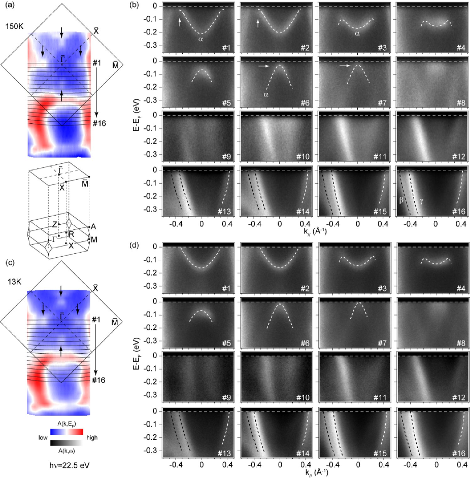
Figures 2(a) and 2(c) show the Fermi surface maps measured with circularly polarized 22.5 eV photons in the tetragonal and triclinic phases, respectively. There are four patches near the point as indicated by the arrows, and two electron pockets around the point. Sixteen cuts from to are presented in Fig. 2(b) to illustrate the electronic structure evolution in the tetragonal phase, and the corresponding data in the triclinic phase are shown in Fig. 2(d). In the tetragonal phase, the parabolic-shaped band in cuts 1-2 around is referred as . The band appears to be -shaped in cuts 3-4. From cut 1 to cut 4, the parabolic part shrinks continuously, and eventually only the inverted parabolic part is observable in cuts 5-7. The evolution of the electronlike bands around are shown in cuts 8-16, many of which are complex due to the rapid change of dispersions. Nonetheless, two bands ( and ) can be resolved as indicated by the dashed curves in cut 16 and will be further elaborated in Fig. 4. The data in the triclinic phase [Fig. 2(d)] are generally similar to those in the tetragonal phase. Nonetheless, we note that already shows some bending near the Fermi energy () in the tetragonal phase as indicated by the arrows on the data taken along cuts 1-2. On the other hand, just passes through without bending in the triclinic phase. Moreover, the band top of is below in cuts 6-7 of Fig. 2(b) as indicated by the arrows, but barely touches in Fig. 2(d), where cuts 6-7 pass through one of the four patches around . Therefore, the four spectral weight patches around [as marked by four arrows in Fig. 2(a)] are due to the residual spectral weight of the band in the tetragonal phase. However, the band shifts up and they evolve into small holelike Fermi surfaces in the triclinic phase. This will be further illustrated in Fig. 3. Of note, from this complete set of data, we do not observe any sign of band folding or splitting like that in the iron pnictides.LXYang ; YZhang ; BZhou ; GDLiu ; ZX_SDW
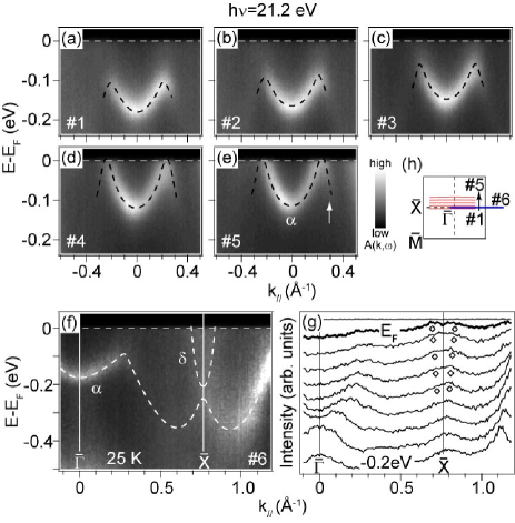
To further illustrate the electronic structure of BaNi2As2, Figs. 3(a)-3(e) present photoemission intensities along five cuts parallel to the - direction in the triclinic phase. The -shaped feature originated from simply moves towards from cut 1 to cut 5, touching at cuts 4-5, which confirms that the four small Fermi surfaces around are holelike. Note that the downward part of [indicated by the arrow in Fig. 3(e)] is clearly resolved here, while it is barely observable in the same momentum region when the cuts are along the - direction, as shown in cuts 1-2 of Figs. 2(b) and 2(d). It highlights the matrix element effects since the 3 orbitals have specific orientations. Figure 3(f) shows the photoemission intensity along -, taken with randomly polarized 21.2 eV photons from a helium lamp in the triclinic phase. The determined band structure is traced by dashed curves, where the broad spectral weight around are attributed to an electronlike band , which is further shown by markers in the corresponding momentum distribution curves (MDCs) [Fig. 3(g)]. Therefore, there is an electron Fermi pocket around .
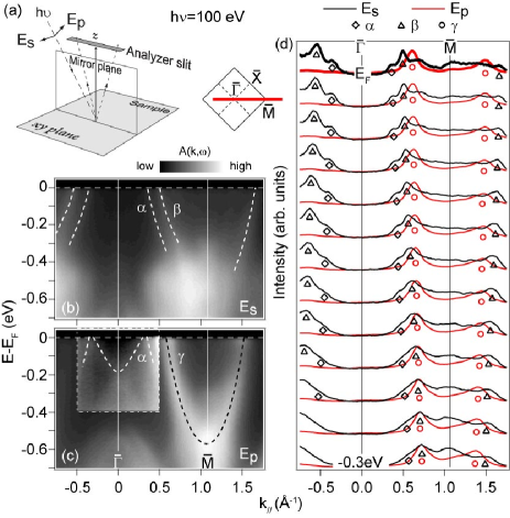
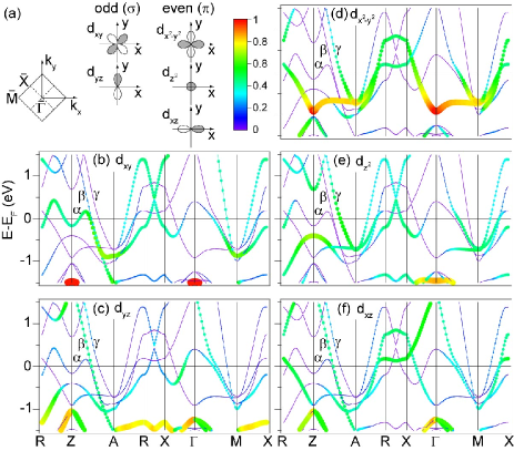
Similar to iron pnictides, the bands near are quite complicated and mainly contributed to by the Ni 3 electrons in BaNi2As2. To resolve the complex bands around , we utilize the linearly polarized light, which could only detect bands with certain symmetry, so that the measured partial electronic structure helps reducing the complexity in analysis.YZhang_orbital Figure 4 presents data along -, taken with linearly polarized 100 eV photons in SLS in the triclinic phase. Two polarization geometries (s and p) are illustrated in Fig. 4(a). In the s polarization geometry, we resolve two bands, whose dispersions are depicted by dashed curves in the photoemission intensity plot [Fig. 4(b)]. While in the p polarization geometry, one intense parabolic electronlike band around is resolved with the band bottom at about -0.57 eV. The dispersions in both geometries are marked in the corresponding MDCs [Fig. 4(d)]. The asymmetry of the dispersion indicated by triangles may be due to the slight sample misalignment. The image contrast in the dash-dotted region in Fig. 4(c) is adjusted to highlight the feature. The observed feature is consistent with the data in Figs. 2 and 3. By comparing with the Fermi crossings observed in cuts 1 and 16 of Fig. 2(d), we attribute the three bands to , , and as shown in Fig. 4(d), where and are two electronlike bands around . Moreover, since the experimental setup under the s (p) polarization geometry detects states with odd (even) symmetry with respect to the mirror plane, the band is of mainly odd symmetry while is of even symmetry. We note that is observed in both geometries [Fig. 4(b) and 4(c)], suggesting that the band has mixed symmetries.
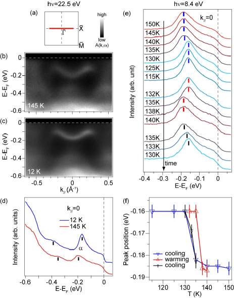
To study the first order transition of BaNi2As2, the temperature dependence is presented in Fig. 5. The photoemission intensity plots along - are shown in Figs. 5(b) and 5(c) for the tetragonal and the triclinic phases respectively. The corresponding energy distribution curves (EDCs) at =0 are stacked in Fig. 5(d). Interestingly, the band bottom of the -shaped feature is moved from -200 meV in the tetragonal phase to -170 meV in the triclinic phase. In other words, the -shaped band moves towards and its electronic energy is raised up. However, another feature at higher binding energies shifts away from . Its band top is moved from -350 meV at 145 K to -390 meV at 12 K, which partially saves the electronic energy. Since the resistivity shows a hysteresis loop,Ronning it is intriguing to investigate whether a similar hysteresis could be observed for the electronic structure. Data in Figs. 5(e)-5(f) are taken with randomly polarized 8.4 eV photons from a xenon discharge lamp, in a cooling-warming-cooling cycle. The EDCs at =0 across the transition are stacked in Fig. 5(e), where the peak positions are indicated by short bars. The temperature dependence of peak positions is summarized in Fig. 5(f), showing a clear hysteresis with the band shift as much as 25 meV. Such electronic structure demonstration of a hysteresis of 3 K is so far the most obvious. A hysteresis in the electronic structure has been observed in FeTe, but with a loop width of only 0.5 K.YZhang_FeTe Our observation here is consistent with the bulk transport properties, which indicates that the measured electronic structure reflects the bulk properties.
IV Band structure calculations
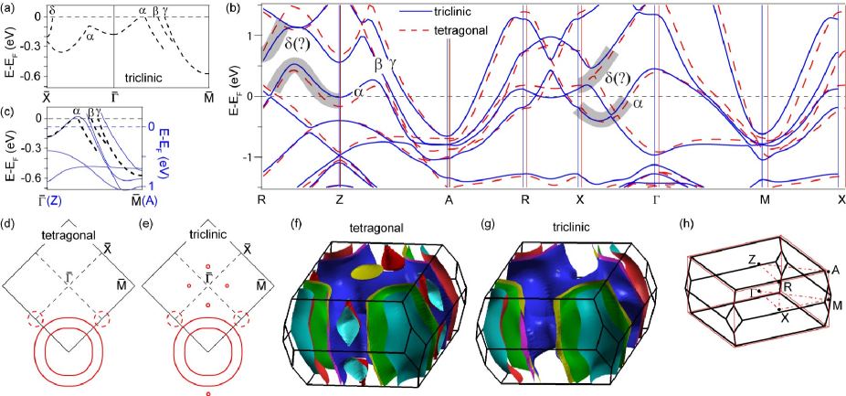
The measured band structure and Fermi surface are summarized in Figs. 6(a), 6(d) and 6(e). For comparison, local density approximation calculations which have been reported before in Ref. optical, are reproduced in Figs. 6(b), 6(f) and 6(g). The notations for bands near are labeled in Figs. 6(a) and 6(b). Qualitatively, although not all calculated bands were observed, the main features of the experiments are captured by the calculation, such as the dispersion nature of the bands. The , , and bands of the experimental results in the - direction are similar to the numerical results in the - direction. As shown in Fig. 6(c), the measured band along - matches the calculation well after the calculated bands are renormalized by a factor of 1.66 and shifted down by 0.08 eV. This renormalization factor is consistent with the results of optical measurements.optical Although not all bands could match, it may suggest that the correlation in BaNi2As2 is weaker than that in iron pnictides.ZX_SDW ; FChen_FeTeSe Along -, the observed and bands partially resemble the calculated dispersions along both - and -, as highlighted by the shaded regions [Fig. 6(b)], but the energy positions do not match. Our data along in this direction might correspond to a between and .
As expected from the differences in the experimentally determined and calculated band structures, the Fermi surface topologies are quite different in both the experiments and the calculations. In our data [Figs. 6(d) and 6(e)], we observe four small Fermi pockets around only in the triclinic phase. Around , two electronlike Fermi pockets are resolved in both phases. Around , the observed Fermi crossings are from an electronlike pocket. As a comparison, in the calculated Fermi surface of high-T tetragonal phase [Figs. 6(f)], there are two large warped cylinders of electron pockets around the zone corner, a pocket interconnected from the zone center to a large deformed cylinder around the zone corner, a 3D electron pocket around , and 3D pockets located between and . In the low-T triclinic phase [Figs. 6(g)], 3D pockets around and between and are gapped out. The large electron Fermi pockets around observed in our data are generally consistent with that in the calculation, which is a direct consequence of two more electrons from Ni than Fe. Note that the -dispersion is significant in the calculation. However, we have measured with four different photon energies, including the more bulk-sensitive 8.4 eV photons, and no obvious differences in dispersion have been observed. Therefore, the -dispersions in BaNi2As2 may be weaker than calculated.
For a multiband and multiorbital superconductor, it is crucial to understand the orbital characters of the band structure. Because of the symmetry of 3 orbitals with respect to the mirror plane, the s polarization geometry in photoemission can only detect the and orbitals while the p polarization geometry can only detect the , , and orbitals [Fig. 7(a)].YZhang_orbital The contributions of the five 3 orbitals to the calculated band structure are presented in Fig. 7(b)-7(f), which therefore can be compared to our polarization dependent data. Along -, the band is consisted of mainly the odd orbital and some contributions of odd and even , thus can be observed in both the s and p polarization geometries; while the band is consisted of the even and orbitals, thus can only be observed in the p polarization geometry. They are in good agreement with our observation. The band is consisted of the odd , and even orbitals in the calculation, thus should be observed in both the s and p polarization geometries. However, is mainly detected in the s polarization geometry, possibly because in the p polarization geometry it is buried in the intense peak of . The consistency between our data and the calculated orbital characters confirms that our data along - match the band structure calculation along -.
V Discussions
It was observed in the optical data that the phase transition leads to a reduction of conducting carriers, consistent with the removal of small Fermi surfaces shown by the calculation.optical However, we do not observe such behavior by ARPES. On the contrary, instead of the disappearance of small Fermi surfaces in the triclinic phase, we observe that bands shift up in energy, leading to additional four Fermi surfaces. The inconsistency between the optical data and our photoemission data suggests that the changes in optical data across the phase transition are possibly an integrated effect of band structure reorganization over the entire Brillouin zone, instead of the disappearance of certain Fermi surface sheets; but it is also possible that only limited -space has been probed in the current photoemission study.
As a sibling compound of iron pnictides, BaNi2As2 exhibits quite different properties and electronic structure. The parent compounds of iron pnictides show a second-order-like transition that is the SDW transition concomitant with a structural transition. However, BaNi2As2 shows a strong first-order-like structural transition, without magnetic ordering reported to date. From the aspect of electronic structure, iron pnictides possess several hole pockets around , and several electron pockets around , but have no pockets around , while the band structure of BaNi2As2 is dramatically different from that of the iron pnictides. Moreover, no signature of folding could be found in our data, confirming that no collinear magnetic ordering exists in BaNi2As2. Because of the intimate relation between the magnetism and superconductivity,Drew_Nat ; Christianson ; LiFeAs_NMR ; Graser the absence of magnetic ordering might be related to the low- in BaNi2As2.
Across the structural transition in BaNi2As2, the Ni-Ni distance changes from 2.93 Å-1 to 2.8 Å-1 (or 3.1 Å-1), corresponding to a lattice distortion as much as 5% in average.Sefat A rough estimation can be made for the hopping parameter between certain - orbitals after the lattice distortion according to Ref. Harrison, ,
where is the relative lattice distortion; is the hopping parameter before the distortion; is the induced hopping parameter change. Therefore, the 5% lattice distortion would cause 17.5% of change to . Since the measured bandwidth of is at least 200 meV, the induced band shift would be larger than 35 meV, more than enough to account for the measured band shift of 25 meV. Note that the differences between the calculated band structures of tetragonal and triclinic phases in Fig. 6(f) are solely induced by considering the different lattice parameters. For instance, the band along - near has a shift of 25% of the bandwidth, generally consistent with our observation. Therefore, our BaNi2As2 data provide a prototypical experimental showcase of band shift due to significant lattice distortion. As a comparison, the lattice distortion in NaFeAs is 0.36%, which would induce only 1 meV of band shift, much smaller than the observed 16 meV by ARPES.CHe Similar results can be found in other iron pnictides.LXYang ; YZhang ; BZhou ; ZX_SDW ; GDLiu The minor lattice distortion cannot account for the large band shift observed in iron pnictides, therefore it has been concluded that the only promising explanation left is that the band shift is related to the magnetism.CHe ; BZhou_SNS
VI Conclusions
To summarize, we report the first electronic structure study of BaNi2As2 by ARPES. In comparison with the band calculation of BaNi2As2 and reports of iron pnictides, we conclude several points as following:
-
i)
We observe four small Fermi pockets around only in the triclinic phase, an electronlike pocket around and two electronlike pockets around in both tetragonal and triclinic phases. The main features of the measured band structure along - is qualitatively captured by the band calculations, however differences exist along -. The electronic structure of BaNi2As2 is also distinct from the that of iron pnictides. Moreover, the correlation effects in BaNi2As2 seems to be weaker than that in iron pnictides, as the band renormalization factor is smaller for BaNi2As2.
-
ii)
Unlike iron pnictides, we do not observe any sign of band folding in BaNi2As2, confirming no collinear SDW related magnetic ordering. Since the magnetism intimately relates to the superconductivity, possibly this is why the is much lower in BaNi2As2 than in iron pnictides.
-
iii)
The SDW/structural transition in iron pnictides is second-order-like, while the structural transition in BaNi2As2 is first-order and a thermal hysteresis is observed for its band shift.
-
iv)
The band shift in BaNi2As2 is caused by the significant lattice distortion. On the other hand, the band shifts in the iron pnictides cannot be accounted for by the minor lattice distortion there, but are related to the magnetic ordering.
Acknowledgements.
Part of this work was performed at the Surface and Interface Spectroscopy beamline, Swiss Light Source, Paul Scherrer Institute, Villigen, Switzerland. We thank C. Hess and F. Dubi for technical support. This work was supported by the NSFC, MOE, MOST (National Basic Research Program No. 2006CB921300 and 2006CB601002), STCSM of China.References
- (1) Y. Kamihara, T. Watanabe, M. Hirano, and H. Hosono, J. Am. Chem. Soc. 130, 3296 (2008).
- (2) X. H. Chen, T. Wu, G. Wu, R. H. Liu, H. Chen, and D. F. Fang, Nature (London) 453, 761 (2008).
- (3) Z. A. Ren, W. Lu, J. Yang, W. Yi, X.-L. Shen, Z. Cai, G.-C. Che, X.-L. Dong, L.-L. Sun, F. Zhou, and Z.-X. Zhao, Chin. Phys. Lett. 25, 2215 (2008).
- (4) R. H. Liu, G. Wu, T. Wu, D. F. Fang, H. Chen, S. Y. Li, K. Liu, Y. L. Xie, X. F. Wang, R. L. Yang, L. Ding, C. He, D. L. Feng, and X. H. Chen, Phys. Rev. Lett. 101, 087001 (2008).
- (5) Chunlei Wang, Zhaoshun Gao, Lei Wang, Yanpeng Qi, Dongliang Wang, Chao Yao, Zhiyu Zhang, and Yanwei Ma, Supercond. Sci. Technol. 23, 055002 (2010).
- (6) Zhi-An Ren , Jie Yang , Wei Lu , Wei Yi , Xiao-Li Shen , Zheng-Cai Li , Guang-Can Che , Xiao-Li Dong , Li-Ling Sun , Fang Zhou, and Zhong-Xian Zhao, EPL 82, 57002 (2008).
- (7) A. Kursumovic, J. H. Durrell, S. K. Chen, and J. L. MacManus-Driscoll, Supercond. Sci. Technol. 23, 025022 (2010).
- (8) Z. A. Ren, J. Yang, W. Lu, W. Yi, G. C. Che, X. L. Dong, L. L. Sun, and Z. X. Zhao, Materials Research Innovations 12, 105, (2008).
- (9) Min Xu, Fei Chen, Cheng He, Hong-Wei Ou, Jia-Feng Zhao and Dong-Lai Feng, Chem. Mater. 20, 7201 (2008).
- (10) Takumi Watanabe, Hiroshi Yanagi, Toshio Kamiya, Yoichi Kamihara, Hidenori Hiramatsu, Masahiro Hirano, and Hideo Hosono, Inorg. Chem. 46, 7719 (2007).
- (11) Zheng Li, Gengfu Chen, Jing Dong, Gang Li, Wanzheng Hu, Dan Wu, Shaokui Su, Ping Zheng, Tao Xiang, Nanlin Wang, and Jianlin Luo, Phys. Rev. B 78, 060504(R) (2008).
- (12) Y. Tomioka, S. Ishida, M. Nakajima, T. Ito, H. Kito, A. Iyo, H. Eisaki, and S. Uchida, Phys. Rev. B 79, 132506 (2009).
- (13) F. Ronning, N. Kurita, E. D. Bauer, B. L. Scott, T. Park, T. Klimczuk, R. Movshovich, and J. D. Thompson, J. Phys.: Condens. Matter 20, 342203 (2008).
- (14) E. D. Bauer, F. Ronning, B. L. Scott, and J. D. Thompson, Phys. Rev. B 78, 172504 (2008).
- (15) M. Rotter, M. Tegel, D. Johrendt, I. Schellenberg, W. Hermes, and R. Pöttgen, Phys. Rev. B 78, 020503(R) (2008).
- (16) T. Yildirim, Phys. Rev. Lett. 101, 057010 (2008).
- (17) Chen Fang, Hong Yao, Wei-Feng Tsai, JiangPing Hu, and Steven A. Kivelson, Phys. Rev. B 77, 224509 (2008).
- (18) Cenke Xu, Markus Müller, and Subir Sachdev, Phys. Rev. B 78, 020501(R) (2008).
- (19) C. He, Y. Zhang, B. P. Xie, X. F. Wang, L. X. Yang, B. Zhou, F. Chen, M. Arita, K. Shimada, H. Namatame, M. Taniguchi, X. H. Chen, J. P. Hu, and D. L. Feng, Phys. Rev. Lett. 105, 117002 (2010).
- (20) L. X. Yang, B. P. Xie, Y. Zhang, C. He, Q. Q. Ge, X. F. Wang, X. H. Chen, M. Arita, J. Jiang, K. Shimada, M. Taniguchi, I. Vobornik, G. Rossi, J. P. Hu, D. H. Lu, Z. X. Shen, Z. Y. Lu, and D. L. Feng, Phys. Rev. B 82, 104519 (2010).
- (21) T. Dong, Z. G. Chen, R. H. Yuan, B. F. Hu, B. Cheng, and N. L. Wang, Phys. Rev. B 82, 054522 (2010).
- (22) Athena S. Sefat, Michael A. McGuire, Rongying Jin, Brian C. Sales, David Mandrus, Filip Ronning, E. D. Bauer, and Yurij Mozharivskyj, Phys. Rev. B 79, 094508 (2009).
- (23) A. J. Drew, Ch. Niedermayer, P. J. Baker, F. L. Pratt, S. J. Blundell, T. Lancaster, R. H. Liu, G. Wu, X. H. Chen, I. Watanabe, V. K. Malik, A. Dubroka, M. Rössle, K. W. Kim, C. Baines, and C. Bernhard, Nat. Mater. 8, 310 (2009).
- (24) A. D. Christianson, E. A. Goremychkin, R. Osborn, S. Rosenkranz, M. D. Lumsden, C. D. Malliakas, I. S. Todorov, H. Claus, D. Y. Chung, M. G. Kanatzidis, R. I. Bewley, and T. Guidi, Nature 456, 930 (2008).
- (25) L. Ma, J. Zhang, G. F. Chen, and Weiqiang Yu, Phys. Rev. B 82, 180501(R) (2010).
- (26) S. Graser, A. F. Kemper, T. A. Maier, H. P. Cheng, P. J. Hirschfeld, and D. J. Scalapino, Phys. Rev. B 81, 214503 (2010).
- (27) M. Yi, D. H. Lu, J. G. Analytis, J.-H. Chu, S.-K. Mo, R.-H. He, M. Hashimoto, R. G. Moore, I. I. Mazin, D. J. Singh, Z. Hussain, I. R. Fisher, and Z.-X. Shen, Phys. Rev. B 80, 174510 (2009).
- (28) Y. Zhang, J. Wei, H. W. Ou, J. F. Zhao, B. Zhou, F. Chen, M. Xu, C. He, G. Wu, H. Chen, M. Arita, K. Shimada, H. Namatame, M. Taniguchi, X. H. Chen, and D. L. Feng, Phys. Rev. Lett. 102, 127003 (2009).
- (29) L. X. Yang, Y. Zhang, H. W. Ou, J. F. Zhao, D. W. Shen, B. Zhou, J. Wei, F. Chen, M. Xu, C. He, Y. Chen, Z. D. Wang, X. F. Wang, T. Wu, G. Wu, X. H. Chen, M. Arita, K. Shimada, M. Taniguchi, Z. Y. Lu, T. Xiang, and D. L. Feng, Phys. Rev. Lett. 102, 107002 (2009).
- (30) Bo Zhou, Yan Zhang, Le-Xian Yang, Min Xu, Cheng He, Fei Chen, Jia-Feng Zhao, Hong-Wei Ou, Jia Wei, Bin-Ping Xie, Tao Wu, Gang Wu, Masashi Arita, Kenya Shimada, Hirofumi Namatame, Masaki Taniguchi, X. H. Chen, and D. L. Feng, Phys. Rev. B 81, 155124 (2010) .
- (31) G.-D. Liu, H.-Y. Liu, L. Zhao, W.-T. Zhang, X.-W. Jia, J.-Q. Meng, X.-L. Dong, J. Zhang, G. F. Chen, G.-L. Wang, Y. Zhou, Y. Zhu, X.-Y. Wang, Z.-Y. Xu, C.-T. Chen, and X. J. Zhou, Phys. Rev. B 80, 134519 (2009).
- (32) Y. Zhang, B. Zhou, F. Chen, J. Wei, M. Xu, L. X. Yang, C. Fang, W. F. Tsai, G. H. Cao, Z. A. Xu, M. Arita, H. Hayashi, J. Jiang, H. Iwasawa, C. H. Hong, K. Shimada, H. Namatame, M. Taniguchi, J. P. Hu, D. L. Feng, arXiv:0904.4022 (unpublished).
- (33) Y. Zhang, F. Chen, C. He, L. X. Yang, B. P. Xie, Y. L. Xie, X. H. Chen, Minghu Fang, M. Arita, K. Shimada, H. Namatame, M. Taniguchi, J. P. Hu, and D. L. Feng, Phys. Rev. B 82, 165113 (2010).
- (34) Z. G. Chen, G. Xu, W. Z. Hu, X. D. Zhang, P. Zheng, G. F. Chen, J. L. Luo, Z. Fang, and N. L. Wang, Phys. Rev. B 80, 094506 (2009).
- (35) Fei Chen, Bo Zhou, Yan Zhang, Jia Wei, Hong-Wei Ou, Jia-Feng Zhao, Cheng He, Qing-Qin Ge, Masashi Arita, Kenya Shimada, Hirofumi Namatame, Masaki Taniguchi, Zhong-Yi Lu, Jiangping Hu, Xiao-Yu Cui, and D. L. Feng, Phys. Rev. B, 81, 014526 (2010).
- (36) W. A. Harrison, : (Dover, New York, 1989).
- (37) Bo Zhou, L. X. Yang, Fei Chen, Min Xu, Tao Wu, Gang Wu, X. H. Chen, and D. L. Feng, \htmladdnormallinkJ. Phys. Chem. Solids.http://dx.doi.org/10.1016/j.jpcs.2010.10.075 (to be published).