Designer switches: Effect of crystal planes on time-dependent electron transport through an interacting quantum dot
Abstract
The time-dependent non-crossing approximation is utilized to determine the effects of the crystal planes of gold contacts on time dependent current through a quantum dot suddenly shifted into the Kondo regime via a gate voltage. For an asymmetrically coupled system, instantaneous conductance exhibits complex fluctuations. We identify the frequencies participating in these fluctuations and they turn out to be proportional to the separation between the sharp features in the density of states and the Fermi level in agreement with previous studies. Based on this observation, we predict that using different crystal planes as electrodes would give rise to drastically different transient currents which can be accessed with ultrafast pump-probe techniques.
pacs:
72.15.Qm, 85.35.-p, 71.15.MbTime-dependent electron transport in single electron devices is a subject of fundamental importance in molecular electronics since it is widely believed that these devices have the potential to replace the conventional MOSFET transistors semiconductor in the near future thanks to the rapid advances in nanotechnology. Detection of electrons in real time LuetAl03Nature is expected to play an important role in development of quantum computers ElzermanetAl04Nature and single electron guns FeveetAl07Science as well.
Time-dependent current arising from sudden switching of the gate or bias voltage NordlanderetAl99PRL ; PlihaletAl00PRB ; MerinoMarston04PRB has been shown to exhibit various time scales PlihaletAl05PRB ; IzmaylovetAl06JPCM . Moreover, interference between the Kondo resonance and the sharp features in the contacts’ density of states emerges in the long timescale associated with the formation of this many-body resonance GokeretAl07JPCM . Effective one-electron theories indicate that the transport properties in steady state depend on the the type of electrode metal KondoetAl09JPCM , the contact-structure KondoetAl06PRB and the indices of crystal planes of electrode metal Wangetal10JAP . Same approach also predicts that the electrode metals would alter the rectifying performance of the device DengetAl09APL .
In previous studies of single electron devices, both the Green’s function techniques ZhuetAl05PRB ; MaciejkoetAl06PRB ; GokeretAl07JPCM and nonequilibrium diagrammatic Monte Carlo method WerneretAl09PRB ; SchmidtetAl08PRB showed that the band structure of the contacts has significant influence on the shape of the transient current. In all these cases, simple unrealistic bands have been used for ease in calculations. In this letter, we will carry out a comparative study using three different crystal planes of gold as contacts to determine the transient current through a single electron device in the Kondo regime. A unique approach which involves using the outcome of an ab-initio calculation as an input in a many-body technique will be adopted.
Single impurity Anderson Hamiltonian representing a discrete spin degenerate level of energy connected to Fermi liquid electrodes describes the physical behaviour of this system adequately. Upon applying the auxiliary boson transformation to the Anderson Hamiltonian, it is transformed into
| (1) | |||||
where operators and with =L,R create(destroy) an electron with spin within the dot and in the left(L) and right(R) contacts respectively. The corresponding number operators are and whereas the hopping amplitude for each contact is denoted with . Operator creates(destroys) a massless boson within the dot and double occupancy is prevented by setting the sum of the number of bosons and the electrons to unity. If one neglects the explicit time dependency of the hopping matrix elements, the coupling of the quantum dot to the contacts can be cast as . In this expression, is a constant determined by and is the density of states of the contacts.
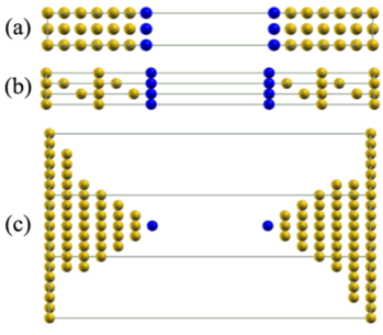
The density-functional theory (DFT) calculations for the density of states (DOS) of the Au contacts have been performed with the full-potential linearized augmented plane wave (FP-LAPW) method using WIEN2K package Blahaetal01Book . As shown in Fig. 1, three geometries, i.e. (001)-surface, (111)-surface and (111)-pyramid, have been adopted to simulate the Au electrode profile. In order to build the structures of these three geometries, atomic slabs with 13 Au layers have been used. The distance between the two opposite electrodes is 30 Bohr radius in all three geometries. The exchange-correlation potential of the generalized gradient approximation within the Perdew, Burke, and Ernzerhof (GGA-PBE) form Perdewetal96PRL has been used in all calculations. The plane wave cut-off has been determined by = 6.5 and = 10. K-mesh of 30x30x3, 36x36x2 and 6x6x2 have been adopted for (001)-surface, (111)-surface and (111)-pyramid respectively. Note that only the DOS of topmost atoms, which are relevant to the transport properties between electrodes in the surface/pyramid structures, will be used in the following many body calculations. The resulting density of states is shown in Fig. 2.
We performed a fitting procedure involving a linear combination of Gaussians given by
| (2) |
to the actual DFT data such that all of the sharp peaks would be captured. An extra broad Gaussian has been added in each case to ensure that the density of states at the Fermi level is non-zero and the entire bandwidth of the material is covered. The outcome of this data fitting procedure that involves Gaussians of varying linewidth and peak position is also shown in Fig. 2 for three different geometries. In the remaining part of this letter, we will shift to atomic units where .
The Dyson equations are solved for the retarded and less than Green’s functions in a discrete two-dimensional grid. This requires the self-energy of electron and massless boson as an input. We use non-crossing approximation to define the self-energies and close these coupled integro-differential equations ShaoetAl194PRB ; IzmaylovetAl06JPCM . The net current follows from the resulting Green’s functions denoted by and . The general expression for the net current JauhoetAl94PRB can be recast by using the slave boson decomposition method GokeretAl07JPCM . The equation we will use in this letter to determine the net current is then written as
| (3) |
where and . In Eq. (3), and are the convolution of with the Fermi-Dirac distributions of contacts and is the Fourier transform of GokeretAl07JPCM . The conductance is equal to the current divided by the bias voltage . In the following discussion , where , will be referred as the asymetry factor.
Kondo effect is a many-body resonance pinned to the Fermi levels of the contacts in the dot density of states and manifests itself as an enhancement in the conductance at low temperatures. The linewidth of the Kondo resonance is characterized by an energy scale (Kondo temperature) given by
| (4) |
where is the half bandwidth of the conduction electrons and .
We will investigate the transient current for the case where the dot level is switched from to at t=0 with a gate voltage. For all three geometries, a transition from a non-Kondo state to a Kondo state takes place. Note that the Kondo temperature in the final state would be slightly lower for (111) pyramide than the other two geometries as a result of shorter conduction electron bandwidth as seen in Fig. 2.
Transient current in Kondo timescale is depicted for all geometries in Fig. 3 after switching to the final dot level in infinitesimal bias. We do not display the short timescale where where the conductance reaches a maximum before it starts to fall off for large asymmetry factors due to striking similarity with previous studies GokeretAl07JPCM . The most remarkable feature is the drastic difference in conductance fluctuations. This effect stems purely from the difference in band structure of the contacts since all other parameters are held constant. We should point out that the slight difference between the Kondo temperature of (111) pyramide and the other two geometries does not change the relative behaviour of the fluctuations for these geometries because is known to alter only the amplitude of the fluctuations GokeretAl07JPCM , not the overall pattern of the transient current.
It is clear that these fluctuations are the result of an admixture of sinusoidal oscillations with different frequencies and amplitudes. Each individual frequency can be extracted by taking the Fourier transform of the current. We found that the frequencies are proportional to the separation between the peak positions and the Fermi level for all cases. This explains why transient current for (001) surface exhibits a more erratic pattern compared to the others as five distinct frequencies are involved in it. Moreover, there are other peaks that appear in actual DFT data but we did not include them in our fitting since they have negligible contribution to the fluctuation pattern. The oscillation amplitude associated with them is probably too small to have a discernible effect because either they are located far away from the Fermi level or the peaks are not prominent compared to the surrounding structure.
The results presented here describes a way to probe the detailed band structure of a molecular switch by measuring the transient current flowing through it. It is possible to capture the transient current fluctuations occurring in the femtosecond timescale with ultrafast pump-probe techniques Teradaetal10JPCM . This would pave the way for designing custom switches for future organic computers.
References
- (1) Committee I R 2004 International Technology Roadmap for Semiconductors (Tokyo: Japan Electronics and Information Technology Industries Association)
- (2) Lu W, Ji Z, Pfeiffer L, West K W and Rimberg A J 2003 Nature 423 422
- (3) Elzerman J M, Hanson R, van Beveren L H W, Witkamp B, Vandersypen L M K and Kouwenhoven L P 2004 Nature 430 431–434
- (4) Feve G, Mahe A, Berroir J M, Kontos T, Placais B, Glattli D C, Cavanna A, Etienne B and Jin Y 2007 Science 316 1169
- (5) Nordlander P, Pustilnik M, Meir Y, Wingreen N S and Langreth D C 1999 Phys. Rev. Lett. 83 808–811
- (6) Plihal M, Langreth D C and Nordlander P 2000 Phys. Rev. B 61 R13341–13344
- (7) Merino J and Marston J B 2004 Phys. Rev. B 69 115304
- (8) Plihal M, Langreth D C and Nordlander P 2005 Phys. Rev. B 71 165321
- (9) Izmaylov A F, Goker A, Friedman B A and Nordlander P 2006 J. Phys.: Condens. Matter 18 8995–9006
- (10) Goker A, Friedman B A and Nordlander P 2007 J. Phys.: Condens. Matter 19 376206
- (11) Kondo H, Nara J, Kino H and Ohno T 2009 J. Phys.:Condens. Matter 21 064220
- (12) Kondo H, Kino H, Nara J, Ozaki T and Ohno T 2006 Phys. Rev. B 73 235323
- (13) Wang L H, Guo Y, Tian C F, Song X P and Ding B J 2010 J. Appl. Phys. 107 103702
- (14) Deng X Q, Zhou J C, Zhang Z H, Tang G P and Qiu M 2009 Appl. Phys. Lett. 95 103113
- (15) Zhu Y, Maciejko J, Ji T, Guo H and Wang J 2005 Phys. Rev. B 71 075317
- (16) Maciejko J, Wang J and Guo H 2006 Phys. Rev. B 74 085324
- (17) Werner P, Oka T and Millis A J 2009 Phys. Rev. B 79 035320
- (18) Schmidt T L, Werner P, Muhlbacher L and Komnik A 2008 Phys. Rev. B 78 235110
- (19) Blaha P, Schwarz K, Madsen G K H, Kvasnicka D and Luitz L 2001 WIEN2K, an augmented plane wave+local orbitals program for calculating crystal properties (Wien: Techn. Universitt)
- (20) Perdew J P, Burke K and Ernzerhof M 1996 Phys. Rev. Lett. 77 3865
- (21) Shao H X, Langreth D C and Nordlander P 1994 Phys. Rev. B 49 13929–13947
- (22) Jauho A P, Wingreen N S and Meir Y 1994 Phys. Rev. B 50 5528
- (23) Terada Y, Yoshida S, Takeuchi O and Shigekawa H 2010 J. Phys.: Condens. Matter 22 264008