Atomic-Scale Compensation Phenomena at Polar Interfaces
Abstract
The interfacial screening charge that arises to compensate electric fields of dielectric or ferroelectric thin films is now recognized as the most important factor in determining the capacitance or polarization of ultrathin ferroelectrics. Here we investigate using aberration-corrected electron microscopy and density functional theory how interfaces cope with the need to terminate ferroelectric polarization. In one case, we show evidence for ionic screening, which has been predicted by theory but never observed. For a ferroelectric film on an insulating substrate, we found that compensation can be mediated by interfacial charge generated, for example, by oxygen vacancies.
pacs:
77.55.hj, 77.22.Ej, 68.37.Ma, 31.15.A-Interfaces between dissimilar materials, especially those with polar discontinuities, often exhibit unusual phenomena. For example, interfacial roughening and atomic diffusion can relieve the diverging electrostatic energy in semiconductor heterointerfaces ref1 . In ferroelectrics, ionic displacements from the nominal high-symmetry lattice sites cause a permanent electrical polarization. As a result, electrical charge appears at the surfaces or interfaces of ferroelectric films that must be compensated by a form of screening ref5 ; ref6 ; ref7 ; ref8 ; ref9 ; ref10 ; ref11 ; ref12 . In ferroelectric films sandwiched between electrodes with perfect metallic screening, conduction electrons screen the surface charges. When the contacting materials are non-ideal metals or insulators, other compensation mechanisms are triggered. One possibility is the formation of domains of opposite polarization ref13 ; ref14 . Another possibility, ionic screening, was recently suggested by theory, but has not been observed ref8 ; ref9 . When a top electrode is not present, it has been found that absorbates or surface point defects provide charge compensation at the free surface of ferroelectric films ref15 ; ref16 ; ref17 ; ref18 ; ref19 . Moreover, it was demonstrated that the polarity of the films could be reversed by varying the oxygen partial pressure over their surfaces ref20 . It is now clear that ferroelectric properties can be controlled by the mechanism by which surface charge is compensated ref12 ; ref15 ; ref16 ; ref17 ; ref21 .
Current understanding of ferroelectric interfaces is based primarily on theory ref7 ; ref8 ; ref9 ; ref10 ; ref22 ; ref23 ; ref24 ; ref25 ; ref26 ; ref27 ; ref28 ; ref28_2 because few experimental techniques have the ability to obtain atomically-resolved measurements of the local atomic displacements that give rise to electric polarization. Only in recent years has it been possible to use phase-contrast high-resolution transmission electron microscopy to obtain local polarization displacements ref29 ; ref30 ; ref31 . Measurements by Jia et al. were used to raise questions about the widely accepted notion that atomic displacements and the tetragonality of the unit cell are directly coupled ref30 ; ref31 ; ref32 . Fong et al. ref33 used X-ray scattering to obtain atomic positions and shed light on the ferroelectric aspects of PbTiO3 on SrTiO3.
In this paper we report phase-contrast images of ferroelectric interfaces obtained simultaneously with high-angle annular dark field images using an aberration-corrected scanning transmission electron microscope (STEM). The data were obtained from regions of the samples that are sufficiently thin (10 nm) to allow the direct extraction of accurate displacements of both light and heavy atoms. This can be shown using image simulations as discussed in the supplemental materials ref42 . We further combine the data with first-principles density-functional calculations to probe compensation mechanisms. Ferroelectric lead zirconate titanate (PZT) on two different substrates were studied - strontium ruthenate (SRO), and strontium titanate (STO). The measured displacements from the PZT/SRO interface reveal a remarkable result. The ionic displacements in the PZT are uniformly bulk-like right up to its interface with SRO. There is no dead layer and no reduction in the polarization in the ferroelectric film at the interface with SRO. The PZT/SRO system, which provides some degree of metallic screening, best lowers its energy by a combination of metallic screening, ionic screening, and domains. The PZT/STO system, however, which lacks metallic screening, can lower its energy by charge compensation at the interface. The calculations indicate that O vacancies can provide appropriate charge compensation, suppressing contributions from ionic screening. Such a role of O vacancies is consistent with recent observations that “missing oxygen surface structures” contribute to the stabilization of a ferroelectric state ref20 .
Ferroelectric films of PbZr0.2Ti0.8O3 (PZT) on a dielectric STO substrate and on a metallic SRO film were investigated. PZT epitaxial films 20 nm thick were grown by pulsed laser deposition (PLD). Details on the sample growth and ferroelectric properties can be found elsewhere ref34 ; ref42 . The structures were examined with an aberration-corrected 300 kV STEM. With aberration correction, the collector angle can be made 10X larger, resulting in an 100X increase in bright-field intensity. This allows the practical collection of high-quality dark-field and bright-field images simultaneously ref35 ; ref42 . The Z-contrast image is used to directly locate the high-atomic-number features such as the Pb, Sr and Ti columns and is thus used to determine the location of the interfaces. The bright field image can be tuned to be sensitive to the lower-atomic-number features such as the O columns.
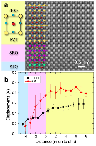
Figure 1(a) shows a phase contrast image seen along the direction of the interfacial region of a ferroelectric PZT film on a thin SRO layer on a STO substrate. In the ferroelectric state, the Pb and Zr/Ti sublattices are shifted relative to the oxygen atoms, as seen in the schematic in Fig. 1(a), leading to a net dipole moment per unit volume. The Pb- and Sr-containing columns are the most prominent features of the images and are thus used to define the reference frame. The displacements of the Zr/Ti and O columns are determined relative to this reference. The atomic positions are determined using an automatic feature location script that determines the “center of mass” of all the bright features in the image. Depending on the feature s relative position, the feature is identified as a Pb/Sr, Ti/Zr or O column. Figure 1(b) contains the measured displacements of Ti/Zr and apical O (O1) columns. Moreover, the PZT film on the metallic SRO layer was found to contain stripe domains of reversed ferroelectric polarization, These domains are commonly referred to as 180∘ stripe domains. The presence of the domains indicate that the thin SRO film (only three unit cells thick), though in principle metallic ref36 ; ref37 , does not provide sufficient free charge to fully screen the depolarizing field. An image of a 1 nm thick domain wall from the PZT film on this SRO layer is included in the supplemental material ref42 . Remarkably, the atomic displacements in the PZT film are relatively constant and bulk-like right up to the interface with SRO. The ionic displacements are seen to continue in the SRO layer. The atoms in the metallic oxide are displaced in the same direction as in the PZT film but the magnitude of the displacements decrease across the thin layer and are zero at the SRO/STO interface. The metallic oxide partially screens the depolarizing field by sharing the ionic displacements of the ferroelectric.
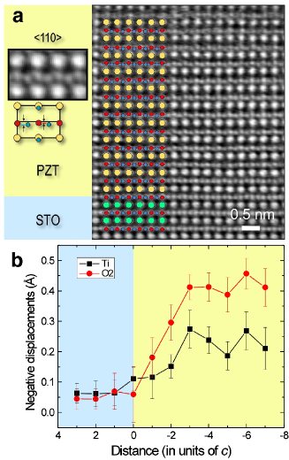
The PZT film on STO was surprisingly found to be monodomain. This has also been seen by Fong el al. ref33 , for metalorganic chemical vapor deposition (MOCVD) grown films slowly cooled to RT. The measured distortions in our PZT films are consistent with bulk-like polarization except for a thin interfacial region. Figure 2 shows an image of a PZT/STO interface and the measured equatorial O (O2) and Ti/Zr column displacements. In this orientation, we have traced the displacement of O2 instead of O1. The reason for this is that it is easier in the view to locate the center of mass of the O2 columns in the horizontal Zr/Ti-O plane than the O1 columns in the vertical Pb-O planes. It is known that the displacement of O2 is larger than that of O1, as we see. Figure 2(a) is a phase-contrast image that shows an arrangement of dipoles that results in the polarization pointing away from the STO substrate, opposite to that seen in the region of the PZT film on SRO/STO in Fig. 1. The displacements in the PZT film are nonzero but are dramatically reduced in the first interfacial layer and then converge to their bulk values within three unit cells of the interface. No statistically significant displacements are found in the STO layers. The depolarizing field is being compensated without forming 180∘ domains on this insulating substrate. Thus, in the absence of metallic screening, ionic screening, or domain structures, there is no evidence for any of the known mechanisms for compensation of the depolarizing field. However, the reduced polarization at the interface means that this interface is charged, and it is charged sufficiently to screen the polarization of PZT. There are not many effects that could do this - a Ti or Pb valence change or oxygen vacancies are physically reasonable reactions especially for films grown by high-energy deposition processes such as pulsed laser deposition. However, reducing the Ti valence from 4+ would reverse the direction of polarization. Therefore, oxygen vacancies or some other source of positive charge is needed. Pb3+ or Pb4+, localized structural modifications to PZT, or holes in the valence band localized at the interface are other possible sources of positive charge. From the profile of the displacements as a function of the distance from the interface, the charge source must exist within the PZT film.
In order to explore this possible alternative compensation mechanism, calculations were performed for a PbTiO3(PTO)/STO superlattice, leaving out the 20% Zr that is present in random Ti positions in PZT. The Zr affects the piezoelectric response of the material, but should have negligible effect on the issues studied here as we previously confirmed ref34 . We carried out first-principles density-functional total-energy calculations using the projector augmented-wave method ref38 as implemented in the VASP code ref39 . The calculations were performed using the local-density approximation (LDA) for the exchange-correlation potential. Supercells were used consisting of six-unit-cell layer of STO and eight-unit-cell layer of PTO, or six-unit-cell layer of SRO and eight-unit-cell layer of PTO. Though the experimental sample had only three unit cells of SRO, we used six in the simuations in order to minimize the interface-interface interactions in our model superlattice. The adequacy of eight unit cells of PTO is confirmed by the fact that the calculated displacements in the middle of the thin film converge to bulk values. To simulate the epitaxial growth of PZT and SRO on STO substrate, the in-plane lattice constant was fixed to the theoretical STO lattice constant of 3.864 Å, and the ionic positions were relaxed so that the force on every ion was less than 2 meV/Å. The average in-plane compressive strain in the SRO layer for these calculations is 0.5%, the same as the experimental value for SRO on STO. When an oxygen vacancy was considered in the calculations, the supercell was doubled in the and (in-plane) directions so that there was one oxygen vacancy for every four interface units.
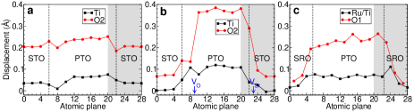
Upon relaxation of the structure, we find that, in agreement with the results of Ref. ref40 ; ref41 , the depolarizing field created by the PTO forces the dielectric STO layer to also become polarized. The atomic displacements are nearly uniform in the PTO/STO superlattice as seen in Fig. 3(a). It is clear, however, from our experimental observations (see e.g. Fig. 2) that something else, not STO polarization, is the compensation mechanism.
The effect of an optimal arrangement of oxygen vacancies is shown in Fig. 3(b). The figure shows that the displacements in the PTO slab are nearly as large as those calculated for bulk PTO, they decay in the PTO layer, and nearly disappear in the STO slab. Results of the total-energy calculations indicate that oxygen vacancies prefer to be located in the ferroelectric PTO layer over STO, prefer the Pb-O planes in the PTO layer to the TiO2 planes and want to be close to the interface. The presence and location of the source of positive charge (O vacancies in our calculations) is the key to compensation.
We now turn to examine theoretical results for the PZT/SRO system, which comprises ferroelectric and metal films. As noted already, in addition to metallic screening, the observed 180∘ domains in PZT/SRO provide further screening of the depolarization field. Our calculations assumed a monodomain superlattice PTO/SRO with short-circuit electrical boundary condition. The ferroelectric displacement in Fig. 3(c) shows that the calculations reproduce the observed induced ionic polarization of the metallic oxide electrode. The calculations support the remarkable experimental observation that the displacements are relatively constant in the PTO layer and decrease to near zero very quickly in the SRO layer. However, the predicted displacements are smaller than the measured values and the values calculated for bulk PTO. The experimental observation that domains of reversed polarization are present in the PZT film indicates that SRO is not able to supply enough free charge to completely screen the depolarizing field. Introducing O and Sr vacancies at the PTO/SRO interfaces increases the atomic displacements nearly to the level of bulk PTO, but the width of the decay region at the interface becomes narrower than what is observed. Segregation of oxygen or Sr vacancies to the PZT/SRO interface does not appear to be necessary. Stripe domains balance the interfacial charge that remains after metallic and ionic screening.
In summary, we have used atomic resolution phase contrast images to accurately measure the small atomic displacements that produce electric polarization in ferroelectrics. Remarkably, the atomic displacements in the PZT film were found to be relatively constant and “bulk-like” right up to the interface with a metallic oxide, SRO. The displacements in the PZT film on an insulating substrate, STO, were found to be nonzero but are dramatically reduced in the first interfacial layer and then converge to their bulk values within three unit cells of the interface. The combination of imaging with first-principles density-functional calculations led to the identification of two very different interfacial reactions to screen the depolarizing field. At the interface between a high-quality PZT film and a metallic oxide layer (SRO), in addition to the metallic screening, we found that ionic screening also occurs in the metallic SRO electrode. Furthermore, these two mechanisms are not sufficient to fully screen the depolarizing field, whereby 180∘ domains in the PZT slab are observed. For the interface between two insulators (PZT and STO), we find that charge compensation is achieved by the segregation of a positive charge source (oxygen vacancies in our calculations) to the ferroelectric side of the interface.
Acknowledgements.
We thank J. T. Luck and A. R. Lupini for important contributions. This research was sponsored by the Materials Sciences and Engineering Division, Office of Basic Energy Sciences, U.S. Department of Energy, by DOE grant DE-FG02-09ER46554, by the McMinn Endowment at Vanderbilt University, and by the ORNL Laboratory Directed Research and Development Program.References
- (1) W. A. Harrison, E. A. Kraut, J. R. Waldrop, and R. W. Grant, Phys. Rev. B 18, 4402 (1978).
- (2) I. P. Batra and B. D. Silverman, Solid State Commun. 11, 291 (1972).
- (3) M. Dawber, P. Chandra, P. B. Littlewood, and J. F. Scott, J. Phys.: Condens. Matter 15, L393 (2003).
- (4) J. Junquera and P. Ghosez, Nature 422, 506 (2003).
- (5) N. Sai, A. M. Kolpak, and A. M. Rappe, Phys. Rev. B 72, 020101 (2005).
- (6) G. Gerra, A. K. Tagantsev, N. Setter, and K. Parlinski, Phys. Rev. Lett. 96, 107603 (2006).
- (7) M. Stengel and N. A. Spaldin, Nature 443, 679 (2006).
- (8) M. E. Lines and A. M. Glass, Principles and applications of ferroelectrics and related materials (Clarendon Press, Oxford, 1977).
- (9) C. H. Ahn, K. M. Rabe, and J. M. Triscone, Science 303, 488 (2004).
- (10) S. K. Streiffer et al., Phys. Rev. Lett. 89, 067601 (2002).
- (11) D. D. Fong et al., Science 304, 1650 (2004).
- (12) Y. Watanabe, M. Okano, and A. Masuda, Phys. Rev. Lett. 86, 332 (2001).
- (13) J. E. Spanier et al., Nano Lett. 6, 735 (2006).
- (14) D. D. Fong et al., Phys. Rev. Lett. 96, 127601 (2006).
- (15) A. M. Kolpak, I. Grinberg, and A. M. Rappe, Phys. Rev. Lett. 98, 166101 (2007).
- (16) D. Li et al., Nature Mater. 7, 473 (2008).
- (17) R. V. Wang et al., Phys. Rev. Lett. 102, 047601 (2009).
- (18) C. Lichtensteiger, J. M. Triscone, J. Junquera, and P. Ghosez, Phys. Rev. Lett. 94, 047603 (2005).
- (19) R. E. Cohen, Ferroelectrics 194, 323 (1997).
- (20) M. Dawber, K. M. Rabe, and J. F. Scott, Rev. Mod. Phys. 77, 1083 (2005).
- (21) A. M. Kolpak, N. Sai, and A. M. Rappe, Phys. Rev. B 74, 054112 (2006).
- (22) B. Meyer and D. Vanderbilt, Phys. Rev. B 63, 205426 (2001).
- (23) F. Y. Rao et al., Phys. Rev. B 55, 13953 (1997).
- (24) M. Stengel, D. Vanderbilt, and N. A. Spaldin, Nature Mater. 8, 392 (2009).
- (25) S. Prosandeev and L. Bellaiche, Phys. Rev. B 75, 172109 (2007).
- (26) P. Aguado-Puente and J. Junquera, Phys. Rev. Lett. 100, 177601 (2008).
- (27) W. Tian et al., in Materials Research Society Symposium Proceedings, Vol. 655: Ferroelectric Thin Film IX, edited by P. C. McIntyre et al., page CC7.8.
- (28) C. L. Jia et al., Nature Mater. 6, 64 (2007).
- (29) C. L. Jia et al., Nature Mater. 7, 57 (2008).
- (30) P. Muralt, Nature Mater. 6, 8 (2007).
- (31) D. D. Fong et al., Phys. Rev. B 71, 144112 (2005).
- (32) H. N. Lee et al., Phys. Rev. Lett. 98, 217602 (2007).
- (33) N. Shibata et al., Science 316, 82 (2007).
- (34) Y. N. Chang et al., Phys. Rev. Lett. 103, 057201 (2009).
- (35) J. M. Rondinelli et al., Phys. Rev. B 78, 155107 (2008).
- (36) G. Kresse and D. Joubert, Phys. Rev. B 59, 1758 (1999).
- (37) G. Kresse and J. Furthmüller, Phys. Rev. B 54, 11169 (1996).
- (38) J. B. Neaton and K. M. Rabe, Appl. Phys. Lett. 82, 1586 (2003).
- (39) M. Dawber et al., Phys. Rev. Lett. 95, 177601 (2005).
- (40) See supplementary material for additional experimental and calculation details.