Proposal for electron quantum spin Talbot effect
Abstract
We propose a quantum spin Talbot effect for an electron beam transmitted through a grating of magnetic nanostructures. Tunable periodic magnetic nanostructures can be used in conjunction with electron-beam illumination to create a spin polarized replica of the transversely periodic exit surface beam a Talbot length away, due to quantum interference. Experiments have been proposed to verify the effect in a two dimensional electron gas. This effect provides a new route to modulate electron spin distributions without a magnetic field. A quantum spin Talbot interferometer and transistor are proposed for spintronics applications.
pacs:
75.76.+j, 75.70.Rf, 72.25.-b, 03.75.-b, 42.25.JaThe ability to tune scalable semiconductor-based spintronics devices, based on the intrinsic spin of electrons to store and manipulate information, is both important and highly challenging for spin-based electronics since spin injection, spin accumulation and spin modulation of electrons are required peter ; albert ; prinz1 ; prinz2 ; wolf . Currently, manipulation of the spin during transport between injector and detector via spin precession and spin pumping can be accomplished spin , however, those methods have difficulty controlling spin distributions. By contrast, local tunability of spin distributions over nanometer scales is crucial for future solid state quantum computers based on electron spin andrea . Inspired by the progress in fabricating and controlling nanoscale magnetic structures parkin , we propose a spin-dependent quantum Talbot effect for electron waves transmitted by a grating composed of magnetic nanostructures, to modulate the spin lattice pattern formed from a spin polarized replica of the structure upon propagation through a Talbot length period and adjustable by controlling the electron wavelength and magnetic nanostructures’ period. This leads to potential applications such as a quantum spin Talbot transistor and a quantum spin Talbot interferometer.
The optical Talbot effect was discovered in 1836 Talbot , and later explained by Rayleigh as a natural consequence of Fresnel diffraction. He showed that the Talbot length T is given by = Rayleigh , in the paraxial approximation , where is period of the grating and is the wavelength of the incident light. However, in a non-paraxial regime where 2, the Talbot effect is also operative for nonevanescent components of the scattered beam eero . This effect reveals the wave-nature of both radiation and matter wave fields, examples of the latter including atoms, electrons and plasmons chapman ; cronin ; benjamin ; eero ; dennis ; leskova .
In this Letter, we calculate a spin polarized non-paraxial Talbot effect for electron matter waves transmitted through a grating composed of magnetic nanostructures. We find that the spin asymmetry of the transmitted field varies with distance from the grating, creating an electron spin replica of the structure a Talbot length away, in a non-paraxial regime where 2. This creates a tunable spin lattice in two-dimensional space, which is a powerful method to manipulate electron spin distributions in solid state systems. We find that the quantum spin interference pattern strongly depends on the wavelength and grating period. Based on our theoretical results, we propose experiments to verify this quantum spin Talbot effect (QSTE) in a two dimensional electron gas (2DEG) system and an atomically flat surface by spin polarized scanning probe microscopy. We propose both a quantum spin Talbot interferometer (QSTI) and quantum spin Talbot transistor (QSTT) devices.
For a grating with period , normally illuminated with a monoenergetic electron plane wave, the two-component spatial electron wave function at energy and at any distance downstream of the exit surface is
| (1) |
Here, is the transverse coordinate, denotes the Fourier coefficients of the two independent electron spin projections, =, and m= eero ; dennis ; leskova , is the de Broglie wavelength, is Planck’s constant and is the electron mass. and represents “spin up”and “spin down” states of electron spin, respectively.
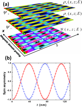
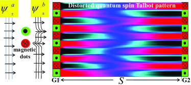
Consider a grating formed by nanoscale magnetic structures, for example, magnetic stripe domains, as shown in Fig. 1. Electron waves have a different complex transmission coefficient depending on the configuration of the incoming electron beam spin state relative to the magnetization direction of magnetic domains (parallel (, ) or anti-parallel (, )) peter ; albert ; wolf . Consequently, the spin up (down) electron wave () propagates through the up (down) magnetic domains in the grating, therefore achieving separation of the electron wave depending on the spin state is expected as shown in Fig. 1(a). The electron wave passes through the magnetic “up” domains (green) with 100% transmission while being blocked completely by domains (red). The color denotes the magnetization direction of a single domain. The corresponding probability density diffracted from the magnetic grating is longitudinally periodic in with period . Simultaneously, the probability density depends on the spin of the electron wave shown in Fig. 1(a), as given by:
| (2) |
where
| (3) |
By definition, the spin asymmetry ( -)/( +) will have the same longitudinal periodicity as the probability density. Since both the numerator and the denominator have a longitudinal periodicity equal to the Talbot distance, when either or 2, implies a continuously tunable spin lattice in two dimensional space as shown in Fig. 1(b). The distribution of two-dimensional spin asymmetry is determined by and . In Fig. 1, =10 nm and =20 nm; the numerically calculated Talbot distance T is 75 nm instead of 80 nm as expected by the conventional formula 22/. The discrepancy is due to the paraxial approximation in conventional Talbot theory. To calculate the non-paraxial T by the self-imaging condition (,T;)=(,0;), for integer and 2, we obtain
eero ,
| (4) |
From Eq. 4, T= 74.6 nm, consistent with our numerical results based on Eqs. 2–4. For the paraxial approximation , Eq. 4 approaches 22/, consistent with the literature eero ; dennis ; leskova . The spin asymmetry distribution (Fig. 1 (b)) in the range 0.5, where =/, is
| (5) |
where (x)=+2()-1. Note that evanescent waves have been neglected in calculating the above expression. If = /4, then 0.97 as shown in Fig. 1(b). Therefore, spin lattices can be tailored through nm to sub-m depending on and .
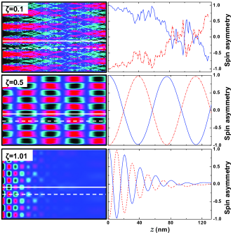
To understand this tunability, we calculated the QSTE for different . We find that the spin asymmetry profile curves show a simple sine relationship when 0.5. However, if , the curves have complex structures and small ripples decorate the spin asymmetry distribution (e.g. = 0.1); when 1, evanescent waves imply that the polarization of spin decreases exponentially along (e.g. = 1.01); Eqs. 4 and 5 are not applicable for these ranges. Movie 1 shows sequential evolution of the and with at = 20 nm movie1 .
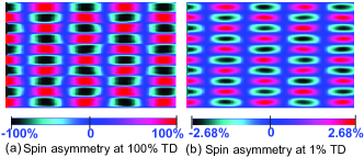
In a more realistic model, the electron wave undergoes partial transmission at the antiparallel configuration between spin orientation and magnetization direction of the domain. Considering this, we find that the probability density distributions are blurred but nevertheless distinguishable; even assuming only 1% transmission difference (TD) between two channels. The intensity contrast and spin polarization drop with TD by the same order of magnitude (Fig. 3).
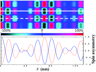
For a finite energy spread, assume an incident distribution of electron energies . Under this model, we obtain (,)(,;)/. The influence of energy spread on the 2D QSTE is calculated by numerical evaluation of (,), assuming to be uniform from =15 nm to 20 nm, with the results shown in Fig. 4. Surprisingly, a dramatic longitudinal modulation of spin polarization near the grating is observed. Consequently, the spin Talbot distance is also modulated depending on the energy spread . In Fig. 4, instead of one peak appearing within each spin Talbot distance, multiple peaks appear. Therefore, to verify the QSTE, a narrow energy spread is desired, or the method should have high energy resolution to distinguish different energy channels.
A 2DEG at interfaces such as in a AlGaAs/GaAs heterostructure is a candidate for testing the effect due to the small energy spread at the Fermi level. In addition, the high mobility of electrons ( 3x106 cm2V-1s-1) and their long spin transportation distance ( hundred m) are suitable properties for spatial imaging of this effect holland ; DD ; wolf ; TP ; mark . The electron de Broglie wavelength at the Fermi energy is unusually long, around 20–100 nm TP , making it easy to design a suitable magnetic domain period and minimize effects caused by nonzero domain wall width schmid ; wxtang . Further concern includes suitable materials for the grating formed by magnetic stripe domains. The wavelength of electrons in metal is normally less than 1 nm, therefore, dilute magnetic semiconductors such as MnGaAs might be suitable to form magnetic domain gratings with similar band structure to AlGaAs/GaAs. Furthermore, by applying a pulsed electron current along the grating, the period is tunable by domain wall motion in ns shinjo ; parkin .
We have described the properties of a 2DEG system for testing the effect, however, a spin dependent spatial imaging method is needed. A spatial imaging technique has been elegantly applied in spin Hall-effect detection in a 2DEG system by Scanning Magneto-optic Kerr microscopy (SMOKE) spinhallmoke . This is an ideal way to demonstrate the QSTE.
Besides SMOKE, imaging electron flow in a 2DEG at the nanoscale has been achieved based on a scanning probe method mark ; spm . This measure can be applied to verify the QSTE at GaAs/AlGaAs interfaces. In particular, scanning tunnelling microscopy with a spin polarized tip (SP-STM) is an ideal technique for investigating the surface electron wave QSTE binnig ; wiesendanger ; oka , as it provides both spin contrast and atomic resolution. Recently, spin-dependent quantum interference within a Co magnetic nanostructure by SP-STM has been reported oka . Inspired by this experiment, we believe SP-STM could be used to see QSTE on an atomically flat surface by a grating formed by an antiferromagnetic atomic chain. One of the advantages of SP-STM is its high energy resolution in / spin-asymmetry spectra to differentiate energy channels oka .
We note that a far field non-spin electron Talbot interferometer has been achieved benjamin . Given the quantum spin Talbot pattern obtained in our work, it is straightforward to formulate a quantum spin Talbot interferometer (QSTI)(Fig. 5). In contrast to the non-spin Talbot case, the QSTI is very sensitive to the change in magnetization of magnetic dots located at the front of the grating. This is extremely valuable to read out the magnetic configuration of such dots. The QSTI should also be sensitive to map weak magnetic fields in nanoscale.
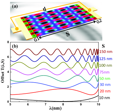
With electrodes connected to two gratings (G1 and G2), a quantum spin Talbot transistor (QSTT) can be fabricated. By calculating the spin transmission probability through the second grating from Eq. 2 as an approximation, we obtain wxt
| (6) |
where is the separation between G1 and G2. The (,) varies from single to multi-peak tuning via and in the range 0.5, exhibiting behavior quite distinct in comparison to both GMR albert and spin Hall effect transistor spinhall . By further including the effect of electric field, we solve the Schrdinger equation with electrical potential, modifying Eq.6 to include an Airy function airy ; however, no dramatic change of the QSTT curve shape is expected wxt .
In conclusion, we propose an electron quantum spin Talbot effect. Potential applications such as the QSTI and QSTT are present. The success of the experiment will provide a new route to actualize periodic spin state distributions in two-dimensional space, also leading to spintronics applications which will be important for future spin-based technologies.
We thank the referees for their insightful comments. WXT thanks Dr. Zheng Gai at ORNL for illuminating discussions on potential experimental realizations, and encouragement.
References
- (1) P. Grunberg, R. Schreiber, Y. Pang, M. B. Brodsky, and H. Sowers, Phys. Rev. Lett. 57, 2442 (1986)
- (2) M. N. Baibich, J. M. Broto, A. Fert, F. Nguyen Van Dau, F. Petroff, P. Etienne, G. Creuzet, A. Friederich, and J. Chazelas, Phys. Rev. Lett. 61, 2472 (1988)
- (3) G. A. Prinz, Phys. Today 48(4), 58 (1995).
- (4) G. A. Prinz, Science 282, 1660 (1998).
- (5) S.A. Wolf, D. D. Awschalom, R. A. Buhrman, J. M. Daughton, S. von Molnar, M. L. Roukes, A. Y. Chtchelkanova, and D. M. Tregar, Science 294, 1488 (2001)
- (6) S. K. Watson, R. M. Potok, C. M. Marcus, and V. Umansky, Phys. Rev. Lett. 91, 258301 (2003)
- (7) A. Morello ., Nature 467, 687 (2010)
- (8) L. Thomas, M. Hayashi, X. Jiang, R. Moriya, Ch. Rettner, and S. S. P. Parkin, Nature 443, 197 (2006)
- (9) H. F. Talbot, Philos. Mag. 9, 401 (1836)
- (10) Lord Rayleigh, Philos. Mag. 11, 196 (1881)
- (11) E. Noponen and J. Turunen, Opt. Commun. 98, 132 (1993)
- (12) M. S. Chapman, et al., Phys. Rev. A 51, R14 (1995)
- (13) A. D. Cronin and B. McMorran, Phys. Rev. A 74, 061602(R) (2006)
- (14) B. J. McMorran and A. D. Cronin, New J. Phys. 11, 033021 (2009)
- (15) M. R. Dennis, N. I. Zheludev, and F. J. G. Abajo, Opt. Express, 15, 9692 (2007)
- (16) A. A. Maradudin and T. A. Leskova, New J. Phys. 11, 033004 (2009)
- (17) In movie 1, the wavelength dependent QSTE is presented.
- (18) N. Rougemaille and A. K. Schmid, Eur. Phys. J. Appl. Phys. 50, 20101 (2010)
- (19) Domain wall width , determined by exchange interaction and anistropy ; ranges from a few nm to m.
- (20) M. C. Holland, A. H. Kean, and C. R. Stanley, J. Crys. Growth 127, 793 (1993)
- (21) D. D. Awschalom, Physica E 10, 1 (2001)
- (22) T. Chakraborty, P. Pietilainen, eds., The Quantum Hall Effects: Integral and Fractional, 2nd ed., Springer-Verlag, New York (1995)
- (23) M. A. Topinka, R. M. Westervelt, and E. J. Heller, Phys. Today 56(12), 47 (2003)
- (24) A. Dourlat, C. Gourdon, V. Jeudy, K. Khazen, H. J. voon Bardeleben, L. Thevenard, and A. Lemaitre, Physica E 40, 1848 (2008)
- (25) A. Yamaguchi, T. Ono, S. Nasu, K. Miyake, K. Mibu, and T. Shinjo, Phys. Rev. Lett. 92, 077205 (2004)
- (26) V. Sih, R. C. Myers, Y. K. Kato, W. H. Lau, A. C. Gossards, and D. D. Awschalom, Nature Phys. 1, 31 (2005)
- (27) M. A. Topinka, B. J. LeRoy, S. E. J. Shaw, E. J. Heller, R. M. Westervelt, K. D. Maranowski, and A. C. Gossard, Science 289, 2323 (2000)
- (28) G. Binnig, H. Rohrer, Ch. Gerber, and E. Weibel, Appl. Phys. Lett. 40, 178 (1982)
- (29) R. Wiesendanger, H.-J. Guntherodt, G. Guntherodt, R. J. Gambino, and R. Ruf, Phys. Rev. Lett. 65, 247 (1990)
- (30) H. Oka, et al. Science 327, 843 (2010)
- (31) B. J. McMorran and A. D. Cronin, New J. Phys. 11, 033021 (2009)
- (32) J. Wunderlich, et al. Science 330, 1801 (2010)
- (33) D. M. Paganin and W.X. Tang, to be published
- (34) S. M. Kennedy, D. M. Paganin and D. E. Jesson, Am. J. Phys. 76(2), 158 (2007)