A general solution to the Schrödinger-Poission equation for charged hard wall: Application to potential profile of an AlN/GaN barrier structure
Abstract
A general, system-independent formulation of the parabolic Schrödinger-Poisson equation is presented for a charged hard wall in the limit of complete screening by the ground state. It is solved numerically using iteration and asymptotic-boundary conditions. The solution gives a simple relation between the band bending and charge density at an interface. I further develop approximative analytical forms for the potential and wave function, based on properties of the exact solution. Specific tests of the validity of the assumptions leading to the general solution are made. The assumption of complete screening by the ground state is found be a limitation; however, the general solution still provides a fair approximate account of the potential when the bulk is doped. The general solution is further used in a simple model for the potential profile of an AlN/GaN barrier, and gives an approximation which compares well with the solution of the full Schrödinger-Poisson equation.
pacs:
73.20.-r,71.20.Nr,74.78.Fk,03.65.-wQuasi two-dimensional electron gases (2DEGs) form at many planar interfaces and surfaces where electron accumulate in inversion layers. Sch ; Ando et al. (1982) They play a central role for the operation of many devices, for instance for metal-oxide semiconductor (MOS) devices, and high-electron mobility transistors (HEMT). Naturally, their properties such as quantized levels and conduction band bending have been much studied both experimentally and theoretically.Fang and Howard (1966); Stern and Howard (1967); Duke (1967); Pals (1972); Klochikhin et al. (2007); Baraff and Appelbaum (1972); King et al. (2008a); Rurali et al. (2008) In particular the angle-resolved photoemission spectroscopy (ARPES) characterisation of the InN surfaces has spurred recent activity. Mahboob et al. (2004); King et al. (2010, 2008b, 2007) Heterojunctions of highly polar materials, such as the III-V nitrides,Smorchkova et al. (2001) induces these 2DEGs at the positively charged interfaces. A good account of the band bending at interfaces in these materials is essential for band-gap engineered intersubband devices such as resonant-tunneling diodes and quantum-cascade lasers. Simple quantum-mechanical systems, such as the particle in box, harmonic oscillator, and linear potential well are instructive model useful to generate rough accounts of various physical phenomena described by the Schrödinger equation. In the same vein, the charged hard wall represent a model case for the Schrödinger-Poission (SP) equation describing the quantization and band bending at interfaces.
The conduction-band edge, or potential, and quantized levels at interfaces are usually obtained with the SP equation with mass , dielectric constant ,
| (1) |
where is the total charge-density comprised of donor, interface, and electron charge. The related textbook linear-potential well problem is inappropriate because it lacks an account of the electron screening inherit to the problem. The SP equation is usually solved iteratively; is updated until it reaches self-consistency. This approach is straightforward to implement, but as a first line of attack to device modelling and for understanding physical trends, simple analytical results are also of great value.
In this paper, a general, system-independent, formulation of the parabolic Schrödinger-Poisson equation for a charged hard wall is presented in the limit of complete screening of the interface charge by the ground-state, that is, in the quantum electrical limit.Baraff and Appelbaum (1972); Pals (1972) It is solved numerically using iteration. These steps follow the earlier work of Pals,Pals (1972) who also provided an analytical approximation using the variational principle. In contrast to Pals, I present analytical expressions that are based on constraints from physical principles and exact properties obtained from the numerical solution. Furthermore, I make specific tests of the general solution outside its expected range of validity. Finally, I demonstrate the usefulness of the analytical expressions for making simple models of the band bending in AlN/GaN heterostrucutes.
A key assumption made to arrive at the model system is the infinite potential barrier or hard wall at . It is appropriate for flat surfaces, as the potential variation is abrupt and the work function is much larger than other characteristic energies; for interfaces, the band offset must be large. Another, is the neglect of non-parabolicity, which is an important effect in some semiconductors, but more-so for excited states of narrow quantum wells than for the ground-state of the shallow quantum wells that form at interfaces.
The assumption of complete screening of the interface charge by the ground state leads to
| (2) |
with for an isotropic 2DEG in zero magnetic field. This assumption is a serious limitation, as it is both a zero-temperature () condition and a restriction on the amount of charge at the interface. For , it is valid when the Fermi level is below the first excited state.
The dimensionless equation that leads to the general solution are obtained with the change of variables: , , and . Here and defines length and an energy scales. The two first change of variables are identical to the textbook procedure for a linear potential well. Mahan (2009) We get
| (3) |
and note that we need only solve this equation once. The system-specific wave function , potential , and ground state eigenvalue can be restored for specific values of , , and .
To guide the computational procedure, I first consider certain limits. For large , , and the asymptote of the wave function follows , which further leads to the asymptote of the potential , where and is the decay factor. For small , the wave function is linear to first order , with , and the first three terms in the expansion of the potential ensues
| (4) |
We can also identify .
The numerical solution of Eq. (3) is obtained using iteration, similar to the solution of the full SP equation. For a given potential , the Schrödinger part is discretized, with uniform grid-spacing according to the finite difference method, and the eigenvalues and eigenvectors are determined with a banded eigenvalue solver.Jones et al. (2001–) equals the minimal eigenvalue and the its normalized eigenvector gives the wave function . Next, using this result as input, the potential is updated until self-consistency is reached. Potential mixing secures convergence. To improve accuracy and simplify extraction of parameters, I use asymptotic boundary conditions (abc): Since, the wave function falls of exponentially, a hard wall boundary condition at for some large cutoff length is commonly used; however, since only a single wave function is retained, the condition can be adopted with being the grid spacing. is updated alongside the potential in the iterative loop. Unlike the hard wall condition, abc guarantees asymptotic behavior at the boundary and can be used to obtain .
| 1/10 | 1/50 | 1/100 | 1/200 | 1/300 | 1/400 | |
| 30 | 2973 | 442.1 | 196.2 | 79.25 | 41.12 | 22.22 |
| 40 | 2414 | 330.8 | 140.6 | 51.46 | 22.60 | 8.329 |
| 50 | 2080 | 264.1 | 107.3 | 34.79 | 11.48 | 0 |
Table 1 shows the result of the convergence study. A grid spacing of and a length of converges within .
| Relation | Parameter | Value |
| 0.70708 | ||
| 1 | ||
| 2.2543 | ||
| -0.25902 | ||
| 1.0179 | ||
| -5.2444 | ||
| 2.3310 | ||
| c | 0.98957 | |
| d | 1.4256 |
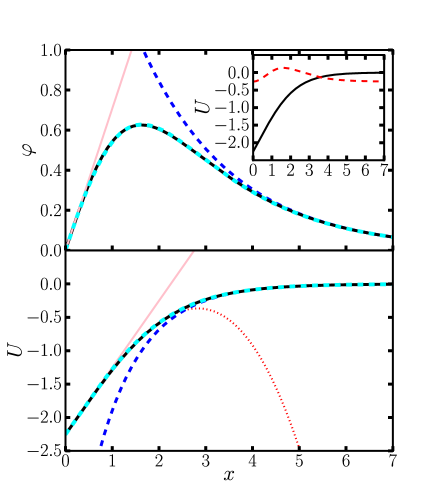
Figure 1 displays the general, system-independent wave function and potential , while table 2 summarizes key parameters. There is only a single bound state; its eigenvalue is . The value of gives a general relation between between the charge at the interface and band banding at : .
Modelling of semiconductor surfaces and interfaces can benefit from analytical approximative expressions of the wave function and potential . I here present such expressions, which are based on constraints stemming from the numerical solution and physical principles. For small , I choose the conditions , and , where , while for large the approximative expressions should have the exact asymptote. Moreover the wave function should be normalized, which follows from charge neutrality. The nodeless shape of the wave function and potential in Fig. 1 motivates simple expressions:
| (5) | ||||
| (6) |
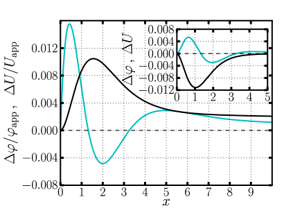
which obeys the specified conditions if and is adjusted to normalize the wave function. Table 2 lists the determined values of and . In Fig. 1 the dashed light curves give the approximative solution, which differ from the numerical by less than the width of the curves. Fig. 2 details the relative difference: and , which is less than 1.6 % for and 1 % for . The insert shows absolute differences. The tiny discrepancy between the approximative and the numerical solution makes the analytical expressions sufficient for most modelling purposes. It also shows that constrained-based strategies can lead to excellent approximative expressions.
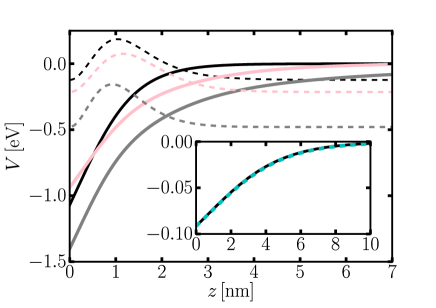
The general solution has a limited range of validity. However, it can still serve as an approximate account of band bending at surfaces and interfaces capturing essential trends and as a building block in simple models. To make a specific test of its robustness, I consider an interface charge of , and bulk that is either undoped or doped to , with other parameters as in GaN. GaN
Fig. 3 displays the result of the robustness test, which show that for this large charge, the general solution is a much better approximation for the potential when bulk is doped, that when it is undoped. This result can be understood as follows: As the first excited state gets occupied, it localizes and significantly increases the effective screening length. With doping, the excited states instead tend to delocalize, and their contribution to the negative charge density partly cancels with the background doping. The complete screening of the interface charge by the ground state is therefore equivalent with the approximation that the charge density of the excited states cancels with that of the bulk donors, which is impossible for zero or tiny donor density. The ground state energy does not typically agree well with that of the general solution. The insert shows that for a fairly small interface charge and low temperature, the general solution agrees well with the solution of the full SP equation yields virtually identical potentials. This agreement also verifies the accuracy and robustness of the numerical solver used and presented in Ref. Berland et al., 2010.
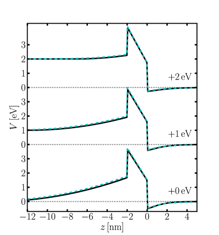
Finally, Fig. 4 illustrates the usefulness of the approximative analytical form given in Eq. (6). It shows the potential profile for a system of a two nanometer wide AlN barrier sandwiched between GaN cladding layers at different bias with bulk doping as before. The full curves give the results of a simple model based on the general solution, while the dashed, the result of a full SP calculations using a step-function for the effective Fermi level. Such profiles are often displayed only for zero bias, perhaps because of the computational complication introduced by a nonconstant Fermi level. To the left of the barrier, a depletion layer forms,Berland et al. (2010); Hermann et al. (2004) which in the simple model is accounted for by a homogeneous charge density equalling the donor density with a depletion length of . The analytical approximation for the potential profile describes the the inversion layer at the right, with an energy and length scale that depends on the charge of the 2DEG . The bias over the structure determines this charge:
| (7) |
where is the charge stemming from the spontaneous and piezoelectric effects. Charge neutrality gives . The full potential profile follows from simple electrostatics. The result using this model agrees well with that of the SP calculation, which shows that the general, system-independent, solution can provide a quick and fairly accurate account of how the polarization in AlN/GaN heterostructures influence the potential profiles.
In summary, the SP equation for a charged hard wall has, in the limit of complete screening by the ground-state, been expressed as a general, dimensionless equation. It leads to a simple relation between the charge at an interface and the conduction band bending. The approximative analytical expressions based on constraints stemming from the exact solution provide a convenient tool for obtaining the potential profile and charge density of heterostructures with large interface charges, such as for AlN/GaN structures. This could aid the design of intersubband devices in these materials.
I thank P. Hyldgaard and T. G. Andersson for helpful discussions. SNIC is acknowledged for supporting my participation in the National Graduate School in Scientific Computing (NGSSC). Financial support from Vinnova (banebrytende IKT).
References
- (1) J.R. Schrieffer, Semiconductor surface physics (University of Pennsylvania Press, Philadelphia, 1957).
- Ando et al. (1982) T. Ando, A. B. Fowler, and F. Stern, Rev. Mod. Phys. 54, 437 (1982).
- Fang and Howard (1966) F. F. Fang and W. E. Howard, Phys. Rev. Lett. 16, 797 (1966).
- Stern and Howard (1967) F. Stern and W. E. Howard, Phys. Rev. 163, 816 (1967).
- Duke (1967) C. B. Duke, Phys. Rev. 159, 632 (1967).
- Pals (1972) J. A. Pals, Phys. Lett. A 39, 101 (1972).
- Klochikhin et al. (2007) A. A. Klochikhin, V. Y. Davydov, I. Y. Strashkova, and S. Gwo, Phys. Rev. B 76, 235325 (2007).
- Baraff and Appelbaum (1972) G. A. Baraff and J. A. Appelbaum, Phys. Rev. B 5, 475 (1972).
- King et al. (2008a) P. D. C. King, T. D. Veal, D. J. Payne, A. Bourlange, R. G. Egdell, and C. F. McConville, Phys. Rev. Lett. 101, 116808 (2008a).
- Rurali et al. (2008) R. Rurali, E. Wachowicz, P. Hyldgaard, and P. Ordejón, Phys. Status Solidi RRL 2, 218 (2008).
- Mahboob et al. (2004) I. Mahboob, T. D. Veal, C. F. McConville, H. Lu, and W. J. Schaff, Phys. Rev. Lett. 92, 036804 (2004).
- King et al. (2010) P. D. C. King, T. D. Veal, C. F. McConville, J. Zúñiga Pérez, V. Muñoz Sanjosé, M. Hopkinson, E. D. L. Rienks, M. F. Jensen, and P. Hofmann, Phys. Rev. Lett. 104, 256803 (2010).
- King et al. (2008b) P. D. C. King, T. D. Veal, and C. F. McConville, Phys. Rev. B 77, 125305 (2008b).
- King et al. (2007) P. D. C. King, T. D. Veal, C. F. McConville, F. Fuchs, J. Furthmüller, F. Bechstedt, P. Schley, R. Goldhahn, J. Schörmann, D. J. As, et al., Appl. Phys. Lett. 91, 092101 (pages 3) (2007).
- Smorchkova et al. (2001) I. P. Smorchkova, L. Chen, T. Mates, L. Shen, S. Heikman, B. Moran, S. Keller, S. P. DenBaars, J. S. Speck, and U. K. Mishra, J. Appl. Phys. 90, 5196 (2001), ISSN 0021-8979.
- Mahan (2009) G. D. Mahan, Quantum mechanics in a nutshell (Princeton Univ. Press, Princeton, NJ, 2009).
- Jones et al. (2001–) E. Jones, T. Oliphant, P. Peterson, et al., SciPy: Open source scientific tools for Python (2001–), URL http://www.scipy.org/.
- Berland et al. (2010) K. Berland, M. Stattin, R. Farivar, D. M. S. Sultan, P. Hyldgaard, A. Larsson, S. M. Wang, and T. G. Andersson, Appl. Phys. Lett. 97, 043507 (pages 3) (2010).
- (19) I. Vurgaftman and J. R. Meyer, Nitride Semiconductor Devices: Principles and Simulation (Wiley-VCH, Weinheim, 2007), Chap. 2. .
- Hermann et al. (2004) M. Hermann, E. Monroy, A. Helman, B. Baur, M. Albrecht, B. Daudin, O. Ambacher, M. Stutzmann, and M. Eickhoff, Phys. Status solidi C 1, 2210 (2004), ISSN 1610-1642.